 | –≠–ª–µ–∫—Ç—Ä–æ–Ω–Ω—ã–π –∫–æ–º–ø–æ–Ω–µ–Ω—Ç: S3842 | –°–∫–∞—á–∞—Ç—å:  PDF PDF  ZIP ZIP |

KSI-8006-003
1
S3842
Current Mode PWM Controller
Descriptions
The S3842, high performance current mode controller, Provides the necessary features to
off-line and DC-DC fixed frequency current control applications offering the designer a cost
effective solution with minimal external components. Internally protection circuity includes
built-in input and reference under-voltage lockout and current limiting with hysteresis.
Also other characteristics of internal circuit provide improved line regulation, enhanced load
response, trimmed oscillation for precise duty cycle control, a temperature compensated
reference, high gain error amplifier, current sensing comparator and totempole output
designed to source and sink high peak current from a capacitive load such as the gate of a
power MOSFET.
Features
∑ Optimized for off-line control ∑ Current mode operation to 500
∑ Low start up and operating current ∑ Under voltage lockout with 6V hysteresis
∑ Pulse by pulse current limiting
∑ Internally trimmed bandgap reference about 5V
∑ Enhanced load response characteristic ∑ Automatic feed forward compensation
Ordering
Information
Type NO. Marking Package Code
S3842 S3842 SOP-8
Outline Dimensions unit :
mm
S
S
e
e
m
m
i
i
c
c
o
o
n
n
d
d
u
u
c
c
t
t
o
o
r
r
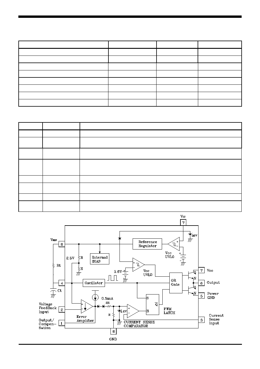
PIN Connections
1. Output / Compensation
2. Voltage feedback. Input
3. Current sense Input
4. Rt/Ct
5. GND
6. Output
7. Vcc
8. Vref
KSI-8006-003
2
S3842
Absolute Maximum Ratings
Ta=25
∞C
Characteristic Symbol
Ratings
Unit
Supply voltage
V
cc
30 V
Current Sense and V
fb
Input
V
IN
-0.3 to V
cc
V
Total Power Supply and Zener Current
I
CC
+ I
Z
30 mA
Output Sink of Source Current
I
o
1 A
Error AMP Output Sink Current
I
eo
10
mA
Operating Ambient Temperature
T
a
0 to 70
∞C
Storage Temperature Range
T
stg
-65 to 150
∞C
Power Dissipation at T
a
50∞C
P
d
1 W
note) All voltages are with respect to PIN5, and current are positive into the specified pin.
PIN Description
PIN NO
Function
Description
1
Compensation Error amplifier output and is made available for loop compensation.
2
Voltage
feedback
Inverting input of error amplifier, normally connected to the switching
power supply output through a resistor driver.
3 Current
sense
A voltage proportional to inductor current is connected to this input.
The PWM uses this information to terminate the output.
4 R
t
/C
t
The oscillator frequency and maximum output duty cycle are
programmed by connecting resistor R
t
to Vref and capacitor C
t
to
ground.
5
Ground
This pin is the combined control circuitry and power ground.
6 Output
This output directly drives the gate of a power MOSFET. Peak current
up to 1.0A are sourced and sinked by this pin.
7 V
CC
This pin is the positive supply of the control IC.
8 Vref
This is the reference output. it provides charging current for capacitor
C
t
through resistor R
t
.
Block Diagram

KSI-8006-003
3
S3842
Electrical Characteristics
(Unless otherwise stated, these specifications apply for 0
Ta
70
∞C;
V
CC
=15V
(Note.4),
R
L
=10 , C
L
=3.3nF
)
Characteristic Symbol
Test
Condition Min.
Typ.
Max.
Unit
1. Reference Section
Output Voltage
Vref
Ta
=25
∞C,
I
O
=1mA
4.90 5.00 5.10
V
Line Regulation
Vref
12V V
CC
25V
- 6 20 mV
Load Regulation
Vref
1mA I
O
20mA
- 6 25 mV
Temperature Stability
V
T
/V
T
(Note 1)
-
0.2
0.4
mV/
∞C
Output Noise Voltage
V
n
10Hz f 10KHz,T
a
=25
∞C(Note
1)
- 50 - uV
Long Term Stability
S
T
a
=125
∞C, 1000Hrs (Note 1)
- 5 - mV
Output Short Circuit
I
SC
-
-30
-100
-180 mA
2. Oscillator Section
Initial Accuracy
f
SC
T
a
=25
∞C
47 52 57 KHz
Voltage Stability
f /V
12 V
a
25V
- 0.05 1.0 %
Temperature Stability
f /T
T
min
T
a
T
max
(Note 1)
- 5 - %
Amplitude V
4
V
PIN4
Peak to Peak
-
1.7
-
V
3. Error Amp Section
Input Voltage
V
2
V
PIN1
=2.5V
2.42 2.50 2.58
V
Input Bias Current
I
b
-
- -0.3
-2.0
Open Loop Voltage Gain
A
VO1
2V V
O
4V
65 90 -
Supply Voltage Rejection
SVR
12V V
a
25V
60 70 -
Output Sink Current
I
O
V
PIN2
=2.7V, V
PIN1
=1.1V 2
6
-
mA
Output Source Current
I
O
V
PIN2
=2.3V, V
PIN1
=5V -0.5
-0.8
-
mA
V
OUT
High V
ch
V
PIN2
=2.3V, R
L
=15 to Ground
5 6 - V
V
OUT
Low V
c1
V
PIN2
=2.7V, R
L
=15 Pin8
- 0.7 1.1 V
4. Current Sense Section
Gain G
V
(Note 2 & 3)
2.8
3.0
3.2
V/V
Maximum Input Signal
V
3
V
PIN 1
=5V (Note 2)
0.9
1.0
1.1
V
Supply Volt Rejection
SVR
12 V
a
25V (Note 2)
- 70 -
Input Bias Current
I
b
-
- -2
-10
5.Output Section
I
SINK
=20mA -
0.1
0.4
V
Output Low Level
V
Ol
I
SINK
=200mA -
1.5
2.2
V
I
SOURCE
=20mA 13.0
13.5
-
V
Output High Level
V
Oh
I
SOURCE
=200mA 12.0
13.5
-
V
Rise time
t
r
T
a
=25
∞C, Cl=1nF (Note 1)
- 50
150 ns
Fall time
t
f
T
a
=25
∞C, Cl=1nF (Note 1)
- 50
150 ns

KSI-8006-003
4
S3842
Electrical Characteristics(continued)
Characteristic Symbol
Test
Condition Min.
Typ.
Max.
Unit
6. Under-Voltage Lockout Section
Start Threshold
V
th
V
PIN7
where
V
PIN8
4.9V
14.5 16.0 17.5
V
Min. Operation Voltage
After Turn-On
V
CC(min)
V
PIN7
where
V
PIN8
1V
8.5 10.0 11.5 V
7. PWM Section
Maximum Duty Cycle
DC
max
-
93 97 100 ns
8. Total Standby Section
Start-Up Current
I
st
V
CC
= 15V before turn on
-
0.4
0.7
mA
Operating Supply Current
I
CC
V
PIN2
=
V
PIN3
=0V
- 11 20 mA
Zener Voltage
V
Z
I
CC
=25mA
- 36 - V
NOTE: 1.Thes parameters, although guaranteed.are not 100% tested in production
2.Parameter measured at trip piont of latch with V
pin2
= 0
3.Gain defined as : A =V
PIN1
/V
PIN3
; 0 V
PIN3
0.8V
4.Adjust V
CC
above the start threshold before setting at 15V
Information in Using IC
1. Under voltage Lockout
To prevent erratic output behavior which activating
the power switch with extraneous leakage currents,
during under voltage lockout. Output(pin6) should be
shunted to ground with a bleeder resister.
The Vcc comparator upper and lower threshold are
16V/10V. The large hysteresis and low start up
currents makes it ideally suited in off-line converter
application where efficient bootstrap start-up
techniques are required.
O N /O F F C O M M A N D
T O R E S E T O F I C
V c c
V o n - 1 6 V
V o f f - 1 0 V
7
V cc
Icc
<17mA
<1mA
10V
16V
KSI-8006-003
5
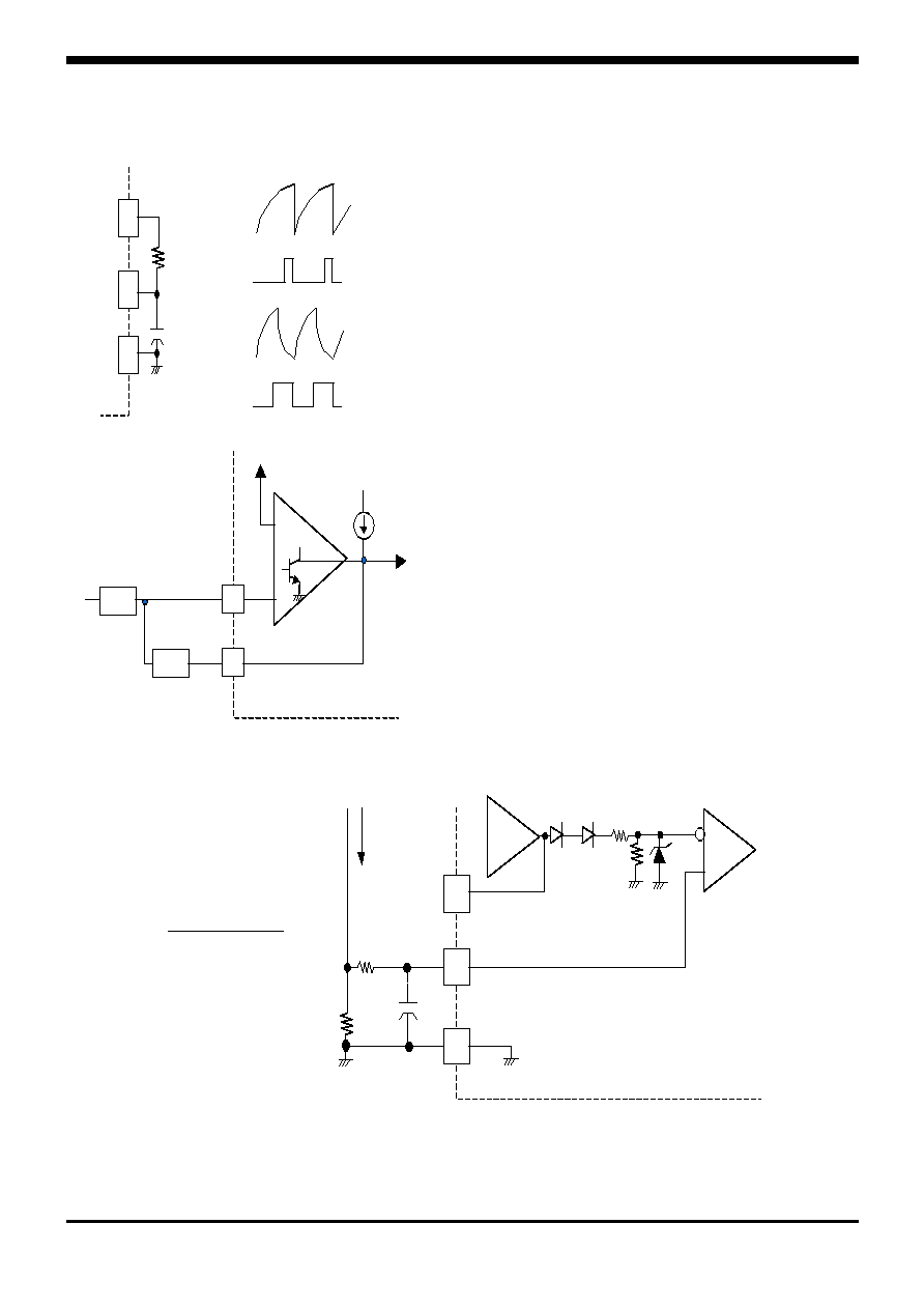
2. Oscillator Waveforms and Maximum Duty Cycle
The oscillator frequency is programmed by the values
selected for the timing components Rt and Ct. Ct is
charged from 5V, Vref, through resistor Rt
to
approximately 2.8V and discharged to 1.2V by an
internal current sink.
During the discharge of Ct, the oscillator generates an
internal blanking pulse and the center input NOR gate high.
This makes output to be in a low state and control the
amount of output dead time.
3. Error AMP Configuration
Error amp output(Pin1) is provided for external loop
Compensation and error amp can source or sink up to 0.5mA.
The non-inverting input is internally biased at 2.5V and is
not pinned out. The converter output voltage is typically
divided down and monitored by the inverting input(pin2).
4. Current Sense Circuit
A normal operating conditions occurs when the power supply output is overloaded or if output voltage to 1.0V
Therefore the maximum peak switch current is lpk(max)=1.0V/R
s
, and under the normal operating conditions the
peak inductor current controlled by the voltage at pin1.
S3842
8
Rt
Ct
4
5
LARGE Rt
SMALL Ct
SMALL Rt
LARGE Ct
Vpin4
INTERNAL
CLOCK
INTERNAL
CLOCK
Vpin4
COMP
ERROR
AMP
1
3
5
GND
CURRENT
SENSE
Rs
R
C
2R
R
IV
I
Ipeak =
R(V pin1 - 2V be)
3R x Rs
0.5mA
2
+
-
1
Zf
Zt
2.50V
V in
COMP
KSI-8006-003
6
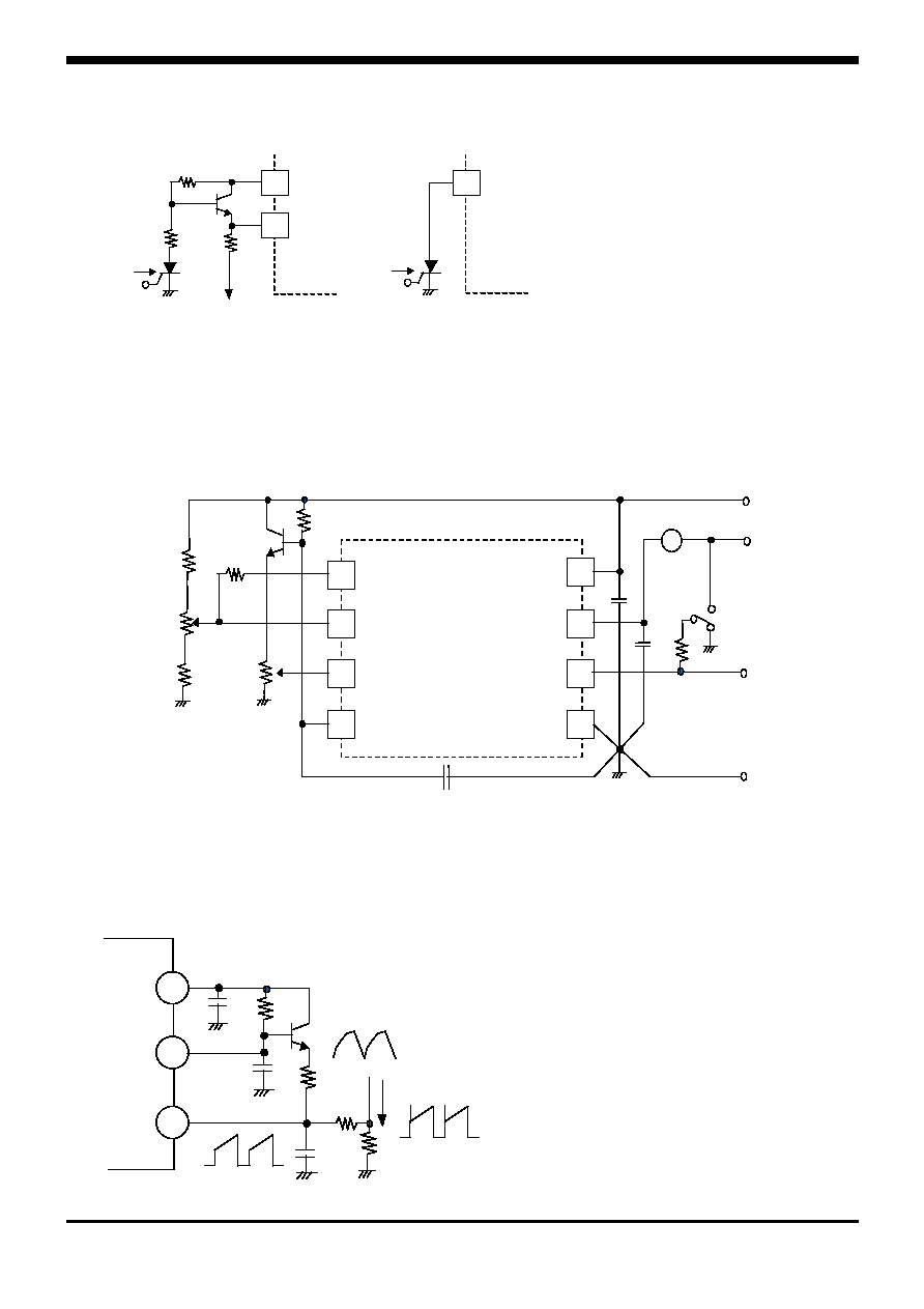
5. Shutdown Techniques
Shutdown of the S3842 can be
accomplished by two methods;
either raise pin3 above 1V or pull
pin1 below a voltage two diodes
drops above ground. Either causes
the output of the PWM method
comparator to be high (refer to
block diagram). The PWM latch is reset dominant so that the output will remain low until the next clock cycle after
the shutdown condition at pins 1 and/or 3 is removed. In one example, an externally latched shutdown may be
accomplished by adding an SCR which turn off, allowing the SCR to reset.
6. Open Loop Test
High peak currents associated with capacitive leads necessitate careful grounding techniques. Timing and bypass
capacitors should be connected close to Pin5 in a single point ground. The transistor and 5 potentiometer are
used to sample the oscillator waveform and apply an adjustable ramp to Pin3.
7. Slope Compensation
A fraction of the oscillator ramp can be resistively
summed with the current sense signal to provide
slope compensation for converters requiring duty
cycle over 50%. Note that capacitor C, forms a
filter with R
2
to suppress the leading edge switch
spikes.
8
4
3
I
S E N S E
R
T
/C
T
V
RE F
I
S E N S E
R
T
C
T
R
1
R
2
C
0.1u F
R
S E N S E
S3842
8
3
V
RE F
I
S E N S E
T O CUR R E NT
S E NS E R ES I S T O R
S HUT
DO W N
4.7K
4.7K
5.00
1
CO MP
S HUT
DO W N
I
SENSE
ADJUST
S3842
V
REF
1
GND
V
REF
I
SENSE
4.7K
COMP
2
3
4
8
7
6
5
Vcc
OUTPUT
GROUND
ERROR
AMP
ADJUST
2N2222
R
T
4.7K
1K
0.1uF
0.1uF
1K/1W
R
T
/C
T
Vin
Vcc
OUTPUT
100K
KSI-8006-003
7
S3842
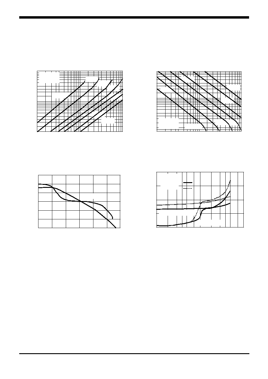
Electrical Characteristic Curves
%DT PERCENT OUTPUT DEAD-TIME
OUTPUT DEAD-TIME vs.
OSCILLATOR FREQUENCY
f
OSC
OS CILLATOR FREQUENCY (KHz )
1.0
2.0
5.0
10
100
50
20
10K
20K
50K
100K
200K
500K 1.0M
V c c =15V
Ta = 25
o
C
Ct =10n F
2.0n F
5.0n F
1.0n F
500pF
200pF
100pF
R
T
T
IM
IN
G
RESISTOR
(
K)
TIMING RESISTOR vs.
OSCILLATOR FREQUENCY
f
OSC
OS CILLATOR FREQUENCY (KHz )
0.8
2.0
5.0
8.0
80
50
20
10K
20K
50K
100K
200K
500K 1.0M
V c c =15V
Ta = 25
o
C
C
T
=10n F
2.0n F
5.0n F
1.0n F
500pF
200pF
100pF
10
100
1K
10K
100K
1M
10M
FREQUENCY (Hz)
VOLTAGE GAIN (dB
)
20
40
60
80
0
Error Amplifier Open-Loop
Frequency Response
PHASE
(
o
)
-135
-90
-45
0
-180
AV
1
2
3
4
0
SA
TUR
A
TION VOLTA
GE (V)
Output Saturation Characteristics
OUTPUT CURRENT SOURCE OR SINK (A)
0.1
0.2
0.3 0.4 0.5 0.7
1
2
3
4
5
7
10
Vcc=15V
Ta = 25
o
C
Ta=-55
o
C
SINK SAT(VOL)
SOURCE SAT(Vcc-VOH)

KSI-8006-003
8
S3842
These AUK products are intended for usage in general electronic equipments(Office and
communication equipment, measuring equipment, domestic electrification, etc.).
Please make sure that you consult with us before you use these AUK products in equipm-
ents which require high quality and/or reliability, and in equipments which could have
major impact to the welfare of human life(atomic energy control, airplane, spaceship, traffic
signal, combustion central, all types of safety device, etc.).
AUK cannot accept liability to any damage which may occur in case these AUK products
were used in the mentioned equipments without prior consultation with AUK.