 | –≠–ª–µ–∫—Ç—Ä–æ–Ω–Ω—ã–π –∫–æ–º–ø–æ–Ω–µ–Ω—Ç: S78L10 | –°–∫–∞—á–∞—Ç—å:  PDF PDF  ZIP ZIP |
KSI-9047-001
1
S78Lxx
Positive-Voltage Regulators
Descriptions
This series of fixed-voltage monolithic integrated-circuit voltage regulators is designed for a
wide range of applications. These applications include on-card regulation for elimination of
Noise and distribution problems associated with single-point regulation. In addition, they
can be used with power-pass elements to make high-current voltage regulators. Each of
These regulators can deliver up to 100mA of output current. The internal limiting and
thermal shutdown features of these regulators make them essentially immune to overload.
When used as a replacement for a Zener diode-resistor combination, on effective
improvement in output impedance can be obtained together with lover-bias current.
Features
∑ 3-Terminal Regulators
∑ Output Current Up to 100mA
∑ No External Components
∑ Internal Thermal Overload Protection
∑ Internal Short-Circuit Limiting
Ordering
Information
Type NO.
Marking
Package Code
S78Lxx
S78Lxx
TO-92
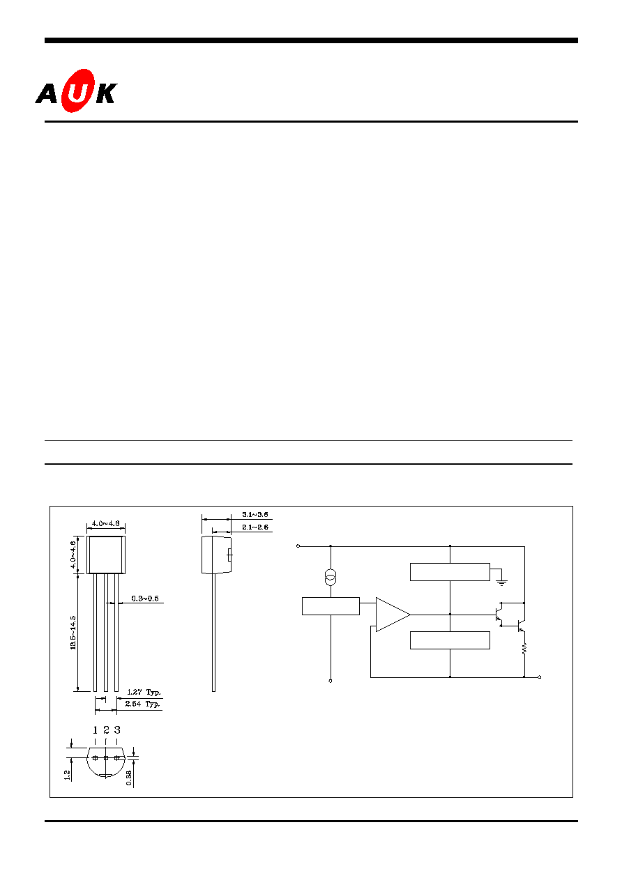
Outline Dimensions unit :
mm
S
S
e
e
m
m
i
i
c
c
o
o
n
n
d
d
u
u
c
c
t
t
o
o
r
r
3
GND
0
Rsc
1
Thermal Shutdown
Circuit
Output
I
Short Circuit
Protection
Input
Reference
Voltage
2
+
-
Block Diagram
PIN Connections
1. Output
2. GND
3. Input

KSI-9047-001
2
S78Lxx
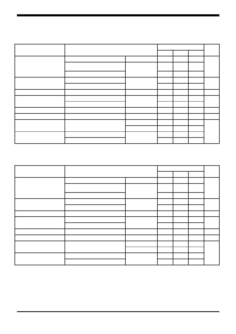
Absolute maximum ratings
(Ta=25
∞C)
Characteristics Symbol
Ratings
Unit
S78L05
Thru
S78L10
30
S78L12
Thru
S78L18
35
Operating Input Voltage
V
IN
S78L24 40
V
Power Dissipation
P
D
625
Operating Temperature Range
T
OPR
-40 ~ +85
Junction Temperature
T
J
150
Storage Temperature Range
T
STG
-55 ~ +150
Lead Temperature Time
T
SOL
260
(10sec)
Recommended operating conditions
Parameter Min.
Max.
Unit
S78L05 7
20
S78L06 8
20
S78L08 10.5
23
S78L09 11.5
24
S78L10 12.5
25
S78L12 14.5
27
S78L15 17.5
30
S78L18 20.5
33
Input Voltage, V
I
S78L24 26.5
39
V
Output current, I
O
100
mA
KSI-9047-001
3
S78Lxx
S78L05 Electrical Characteristics
(V
I
=10V, I
O
=40 , T
J
=0 ~
125 , Unless otherwise noted)
S78L06 Electrical Characteristics
(V
I
=11V, I
O
=40 , T
J
=0 ~
1 25 , Unless otherwise noted)
S78L06
Parameter Test
Conditions*
Min. Typ. Max.
Unit
25
5.75 6 6.25
I
O
=1mA to 40mA
V
I
=8V to 20V
5.7
6
6.3
Output Voltage**
I
O
=1mA to 70mA
0 to 125
5.7 6 6.3
V
V
I
=8V to 20V
35
175
Input regulation
V
I
=9V to 20V
25
29
125
mV
Ripple rejection
V
I
=9V to 19V, f=120Hz
0 to 25
40 48 dB
I
O
=1mA to 100mA
16
80
Output regulation
I
O
=1mA to 40mA
25
9
40
mV
Output noise voltage
f=10Hz to 100KHz
25
46 uV
Dropout Voltage
25
1.7 V
25
3.9 6
Bias current
125
5.5
V
I
=9V to 20V
1.5
Bias Current Change
I
O
=1mA to 40mA
0 to 125
0.1
mA
* Pulse testing techniques are used to maintain the junction temperature as close to the ambient temperature as
possible. Thermal effects must be taken into account separately. All characteristics are measured with a 0.33uF
capacitor across the input and a 0.1uF capacitor across the output.
** This specification applies only for dc power dissipation permitted by absolute maximum ratings.
S78L05
Parameter Test
Conditions*
Min. Typ. Max.
Unit
25
4.8 5 5.2
I
O
=1mA to 40mA
V
I
=7V to 20V
4.75
5
5.25
Output Voltage**
I
O
=1mA to 70mA
0 to 125
4.75 5 5.25
V
V
I
=7V to 20V
32
150
Input regulation
V
I
=8V to 20V
25
26
100
mV
Ripple rejection
V
I
=8V to 18V, f=120Hz
0 to 25
41 49 dB
I
O
=1mA to 100mA
15
60
Output regulation
I
O
=1mA to 40mA
25
8
30
mV
Output noise voltage
f=10Hz to 100KHz
25
42 uV
Dropout Voltage
25
1.7 V
25
3.8 6
Bias current
125
5.5
V
I
=8V to 20V
1.5
Bias Current Change
I
O
=1mA to 40mA
0 to 125
0.1
mA

KSI-9047-001
4
S78Lxx
S78L08 Electrical Characteristics
(V
I
=14V, I
O
=40 , T
J
=0 ~
125 , Unless otherwise noted)
S78L08
Parameter Test
Conditions*
Min. Typ. Max.
Unit
25
7.7 8 8.3
I
O
=1mA to 40mA
V
I
=10.5V to 23V
7.6
8
8.4
Output Voltage**
I
O
=1mA to 70mA
0 to 125
7.6 8 8.4
V
V
I
=10.5V to 23V
42
175
Input regulation
V
I
=11V to 23V
25
36
125
mV
Ripple rejection
V
I
=13V to 23V, f=120Hz
0 to 25
37 46 dB
I
O
=1mA to 100mA
18
80
Output regulation
I
O
=1mA to 40mA
25
10
40
mV
Output noise voltage
f=10Hz to 100KHz
25
54 uV
Dropout Voltage
25
1.7 V
25
4 6
Bias current
125
5.5
V
I
=11V to 23V
1.5
Bias Current Change
I
O
=1mA to 40mA
0 to 125
0.1
mA
S78L09 Electrical Characteristics
(V
I
=16V, I
O
=40 , T
J
=0 ~
125 , Unless otherwise noted)
S78L09
Parameter Test
Conditions*
Min. Typ. Max.
Unit
25
8.6 9 9.4
I
O
=1mA to 40mA
V
I
=12V to 24V
8.55
9
9.45
Output Voltage**
I
O
=1mA to 70mA
0 to 125
8.55 9 9.45
V
V
I
=12V to 24V
45
175
Input regulation
V
I
=13V to 24V
25
40
125
mV
Ripple rejection
V
I
=15V to 25V, f=120Hz
0 to 25
38 45 dB
I
O
=1mA to 100mA
19
90
Output regulation
I
O
=1mA to 40mA
25
11
40
mV
Output noise voltage
f=10Hz to 100KHz
25
58 uV
Dropout Voltage
25
1.7 V
25
4.1 6
Bias current
125
5.5
V
I
=13V to 24V
1.5
Bias Current Change
I
O
=1mA to 40mA
0 to 125
0.1
mA
* Pulse testing techniques are used to maintain the junction temperature as close to the ambient temperature as
possible. Thermal effects must be taken into account separately. All characteristics are measured with a 0.33uF
capacitor across the input and a 0.1uF capacitor across the output.
** This specification applies only for dc power dissipation permitted by absolute maximum ratings.

KSI-9047-001
5
S78Lxx
S78L10 Electrical Characteristics
(V
I
=17V, I
O
=40 , T
J
=0 ~
125 , Unless
otherwise noted)
S78L10
Parameter Test
Conditions*
Min. Typ. Max.
Unit
25
9.6 10 10.4
I
O
=1mA to 40mA
V
I
=13V to 25V
9.5
10
10.5
Output Voltage**
I
O
=1mA to 70mA
0 to 125
9.5 10 10.5
V
V
I
=13V to 25V
51
175
Input regulation
V
I
=14V to 25V
25
42
125
mV
Ripple rejection
V
I
=15V to 25V, f=120Hz
0 to 25
37 44 dB
I
O
=1mA to 100mA
20
90
Output regulation
I
O
=1mA to 40mA
25
11 40
mV
Output noise voltage
f=10Hz to 100KHz
25
62 uV
Dropout Voltage
25
1.7 V
25
4.2 6
Bias current
125
5.5
V
I
=14V to 25V
1.5
Bias Current Change
I
O
=1mA to 40mA
0 to 125
0.1
mA
S78L12 Electrical Characteristics
(V
I
=19V, I
O
=40 , T
J
=0 ~
125 , Unless otherwise noted)
S78L12
Parameter Test
Conditions*
Min. Typ. Max.
Unit
25
11.5 12 12.5
I
O
=1mA to 40mA
V
I
=14V to 27V
11.4
12
12.6
Output Voltage**
I
O
=1mA to 70mA
0 to 125
11.4 12 12.6
V
V
I
=14.5V to 27V
55
250
Input regulation
V
I
=16V to 27V
25
49
200
mV
Ripple rejection
V
I
=15V to 25V, f=120Hz
0 to 25
37 42 dB
I
O
=1mA to 100mA
22
100
Output regulation
I
O
=1mA to 40mA
25
13
50
mV
Output noise voltage
f=10Hz to 100KHz
25
70 uV
Dropout Voltage
25
1.7 V
25
4.3
6.5
Bias current
125
6
V
I
=16V to 27V
1.5
Bias Current Change
I
O
=1mA to 40mA
0 to 125
0.1
mA
* Pulse testing techniques are used to maintain the junction temperature as close to the ambient temperature as
possible. Thermal effects must be taken into account separately. All characteristics are measured with a 0.33uF
capacitor across the input and a 0.1uF capacitor across the output.
** This specification applies only for dc power dissipation permitted by absolute maximum ratings.