 | –≠–ª–µ–∫—Ç—Ä–æ–Ω–Ω—ã–π –∫–æ–º–ø–æ–Ω–µ–Ω—Ç: S7909PI | –°–∫–∞—á–∞—Ç—å:  PDF PDF  ZIP ZIP |

KSI-2026-002
1
S79xxPI
Fixed-Negative-Voltage Regulator
Descriptions
This series of fixed-negative-voltage monolithic integrated-circuit voltage regulators is
designed to complement series S7800 in a wide range of applications. These applications
include on-card regulator for elimination of noise and distribution problems associated with
single point regulations. Each of these regulators can deliver up to 1.0 amperes of output
current. The internal current Limiting and thermal shutdown features of these regulators
make them essentially immune to overload. In addition to use as fixed-voltage regulators,
these device can be used with external components to obtain adjustable output voltages
and also as the power pass element in precision regulators.
Features
∑ Output Current UP to 1.0A
∑ Internal Thermal Overload Protection
∑ Internal Short-Circuit Current Limiting
∑ No External Components
∑ Output Transistor Safe-Area Compensations
Ordering
Information
Type NO. Marking Package Code
S79xxPI S79PI TO-220F
:Voltage Code (05:-5V, 08:-8V, 09:-9V,12:-12V,15:-15V)
Outline Dimensions unit :
mm
S
S
e
e
m
m
i
i
c
c
o
o
n
n
d
d
u
u
c
c
t
t
o
o
r
r
PIN Connections
1. GND
2. Input
3. Output

KSI-2026-002
2
S79xxPI
Absolute Maximum Ratings
Ta=25
∞C
Characteristic Symbol
Ratings
Unit
Operating Input voltage
V
IN
-35 V
Power Dissipation (Tc=25)
P
D
20.8 W
Power Dissipation (without Heatsink)
P
D
2.0 W
Operating Junction Temperature
T
J
-30 ~ 125
∞C
Storage Temperature
T
STG
-55 ~ 150
∞C
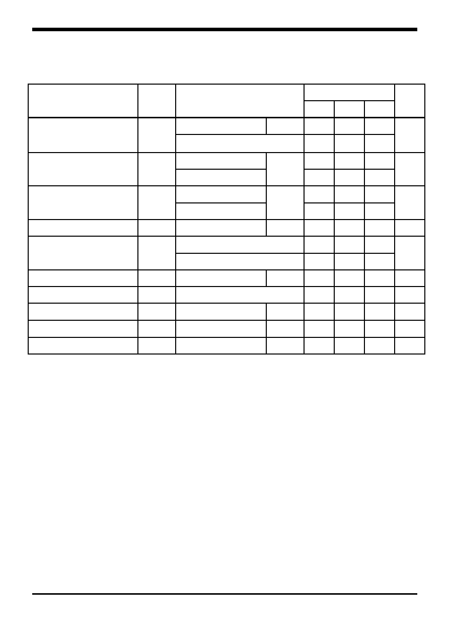
Electrical Characteristics
(T
J
= 0 to 125, Vin= -10V, Iout=500mA, unless otherwise specified.)
S7905PI
Characteristic Symbol Test
Condition
Min. Typ. Max.
Unit
T
j
=25
-4.8 -5.0 -5.2
Output Voltage
V
OUT
I
OUT
=5mA ~ 1A
V
IN
=-7.0V ~ -20V, P
D
15W
-4.75 -5.0 -5.25
V
V
IN
=-7.0V ~ -25V
-
12.5
50
Line Regulation
V
OUT
V
IN
=-8.0V ~ -12V
T
j
=25
- 4 15
mV
I
OUT
=5mA ~ 1.0A
-
15
100
Load Regulation
V
OUT
I
OUT
=250mA ~ 750mA
T
j
=25
- 5 50
mV
Quiescent Current
I
B
T
j
=25
- 1.5 2.0 mA
V
IN
= -7.0V ~ -25
V
- 0.15 0.5
Quiescent Current Change
I
B
I
OUT
= 5mA ~ 1A
-
0.08
0.5
mA
Output Noise Voltage
V
N
f=10Hz ~ 100KHz
T
j
=25
- 125 - uV
rms
Ripple Rejection Ratio
RR
f=120
Hz,
V
IN
=-8.0V ~ -18
V
54 60 - dB
Dropout Voltage
V
D
I
OUT
=1A
T
j
=25
- 2.0 - V
Temperature coefficient of
output Voltage Drift
T
CVO
I
OUT
=5mA -
-0.4
-
mV/
∞C
Peak Output Current
I
PK
T
j
=25
- 2.1 - A
Pulse testing techniques are used to maintain the junction temperature as close to the ambient
temperature as possible. Thermal effects must be taken into separately.
KSI-2026-002
3
S79xxPI
Electrical Characteristics
(T
J
= 0 to 125, Vin= -14V, Iout=500mA, unless otherwise specified.)
S7908PI
Characteristic Symbol
Test
Condition
Min. Typ. Max.
Unit
T
j
=25
-7.7 -8.0 -8.3
Output Voltage
V
OUT
I
OUT
=5mA ~ 1A
V
IN
=-10.5V ~ -23V, P
D
15W
-7.6 -8.0 -8.4
V
V
IN
=-10.5V ~ -25V
-
12.5
160
Line Regulation
V
OUT
V
IN
=-11.0V ~ -17V
T
j
=25
- 4 80
mV
I
OUT
=5mA ~ 1.0A
-
15
160
Load Regulation
V
OUT
I
OUT
=250mA ~ 750mA
T
j
=25
- 5 80
mV
Quiescent Current
I
B
T
j
=25
- 1.5 2.0 mA
V
IN
= -10.5V ~ -25
V
- 0.15 1.0
Quiescent Current Change
I
B
I
OUT
= 5mA ~ 1A
-
0.08
0.5
mA
Output Noise Voltage
V
N
f=10Hz ~ 100KHz
T
j
=25
- 200 - uV
rms
Ripple Rejection Ratio
RR
f=120
Hz,
V
IN
=-11.5V ~ -21.5
V
54 60 - dB
Dropout Voltage
V
D
I
OUT
=1A
T
j
=25
- 2.0 - V
Temperature coefficient of
output Voltage Drift
T
CVO
I
OUT
=5mA
T
j
=25
- -0.6 - mV/
∞C
Peak Output Current
I
PK
T
j
=25
- 2.1 - A
Pulse testing techniques are used to maintain the junction temperature as close to the ambient
temperature as possible. Thermal effects must be taken into separately.

KSI-2026-002
4
S79xxPI
Electrical Characteristics
(T
J
= 0 to 125, Vin= -15V, Iout=500mA, unless otherwise specified.)
S7909PI
Characteristic Symbol Test
Condition
Min. Typ. Max.
Unit
T
j
=25 -8.70 -9.0 -9.30
Output Voltage
V
OUT
I
OUT
=5mA ~ 1A
V
IN
=-11.5V ~ -23V, P
D
15W
-8.60 -9.0 -9.40
V
V
IN
=-10.5V ~ -25V
-
10
180
Line Regulation
V
OUT
V
IN
=-110V ~ -17V
T
j
=25
- 5 90
mV
I
OUT
=5mA ~ 1.A
-
12
180
Load Regulation
V
OUT
I
OUT
=250mA ~ 750mA
T
j
=25
- 4 90
mV
Quiescent Current
I
B
T
j
=25
- 3 6 mA
V
IN
= -11.5V ~ -25
V
- 0.1 1.0
Quiescent Current Change
I
B
I
OUT
= 5mA ~ 1A
-
0.08
0.5
mA
Output Noise Voltage
V
N
f=10Hz ~ 100KHz
T
j
=25
- 175 - uV
rms
Ripple Rejection Ratio
RR
f=120
Hz,
V
IN
=-9.0V ~ -19
V
54 60 - dB
Dropout Voltage
V
D
I
OUT
=1A
T
j
=25
- 2.0 - V
Temperature coefficient of
output Voltage Drift
T
CVO
I
OUT
=5mA
T
j
=25
- -0.4 - mV/
∞C
Peak Output Current
I
PK
T
j
=25
- 2.1 - A
Pulse testing techniques are used to maintain the junction temperature as close to the ambient
temperature as possible. Thermal effects must be taken into separately.

KSI-2026-002
5
S79xxPI
Electrical Characteristics
(T
J
= 0 to 125, Vin= -19V, Iout=500mA, unless otherwise specified.)
S7912PI
Characteristic Symbol Test
Condition
Min. Typ. Max.
Unit
T
j
=25 -11.5 -12.0 -12.5
Output Voltage
V
OUT
I
OUT
=5mA ~ 1A
V
IN
=-14.5V ~ -27V, P
D
15W
-11.4 -12.0 -12.6
V
V
IN
=-14.5V ~ -30V
-
5
80
Line Regulation
V
OUT
V
IN
=-16.0V ~ -22V
T
j
=25
- 3 30
mV
I
OUT
=5mA ~ 1.0A
-
15
200
Load Regulation
V
OUT
I
OUT
=250mA ~ 750mA
T
j
=25
- 5 75
mV
Quiescent Current
I
B
T
j
=25
- 2.0 3.0 mA
V
IN
= -14.5V ~ -30
V
- 0.04 0.5
Quiescent Current Change
I
B
I
OUT
= 5mA ~ 1A
-
0.08
0.5
mA
Output Noise Voltage
V
N
f=10Hz ~ 100KHz,
T
j
=25
- 300 - uV
rms
Ripple Rejection Ratio
RR
f=120
Hz,
V
IN
=-15V ~ -25
V
54 60 - dB
Dropout Voltage
V
D
I
OUT
=1A
T
j
=25
- 2.0 - V
Temperature coefficient of
output Voltage Drift
T
CVO
I
OUT
=5mA
T
j
=25
- -0.8 - mV/
∞C
Peak Output Current
I
PK
T
j
=25
- 2.1 - A
Pulse testing techniques are used to maintain the junction temperature as close to the ambient
temperature as possible. Thermal effects must be taken into separately.