 | –≠–ª–µ–∫—Ç—Ä–æ–Ω–Ω—ã–π –∫–æ–º–ø–æ–Ω–µ–Ω—Ç: SA1316-E | –°–∫–∞—á–∞—Ç—å:  PDF PDF  ZIP ZIP |
KSD-O8G008-001
1
SA1316-E
Chip LED
Features
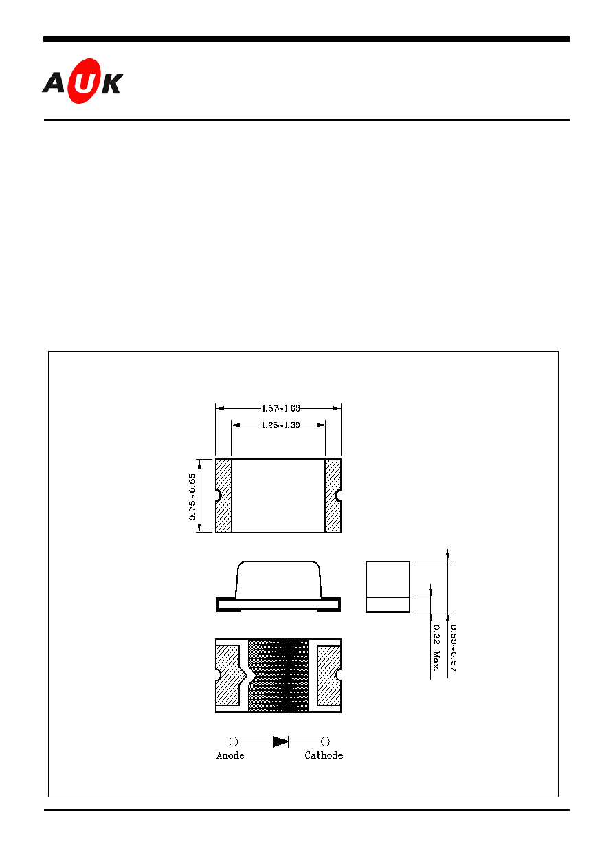
∑ 1.6mm(L)◊0.8mm(W) small size surface mount type
∑ Thin package of 0.55mm(H) thickness
∑ Transparent clear lens optic
∑ Low power consumption type chip LED
Applications
∑ LCD backlighting
∑ Keypad backlighting
∑ Symbol backlighting
∑ Front panel indicator lamp
Outline Dimensions unit :
mm
S
S
e
e
m
m
i
i
c
c
o
o
n
n
d
d
u
u
c
c
t
t
o
o
r
r
KSD-O8G008-001
2
SA1316-E
Absolute Maximum Ratings
(Ta=25
o
C)
Characteristic Symbol
Rating
Unit
Power dissipation
P
D
60
mW
Forward current
I
F
25
mA
*
1
Peak forward current
I
FP
50
mA
Reverse voltage
V
R
4 V
Operating temperature range
T
opr
-2580
∞C
Storage temperature range
T
stg
-30100
∞C
*
2
Soldering temperature
T
sol
240∞C for 10 seconds
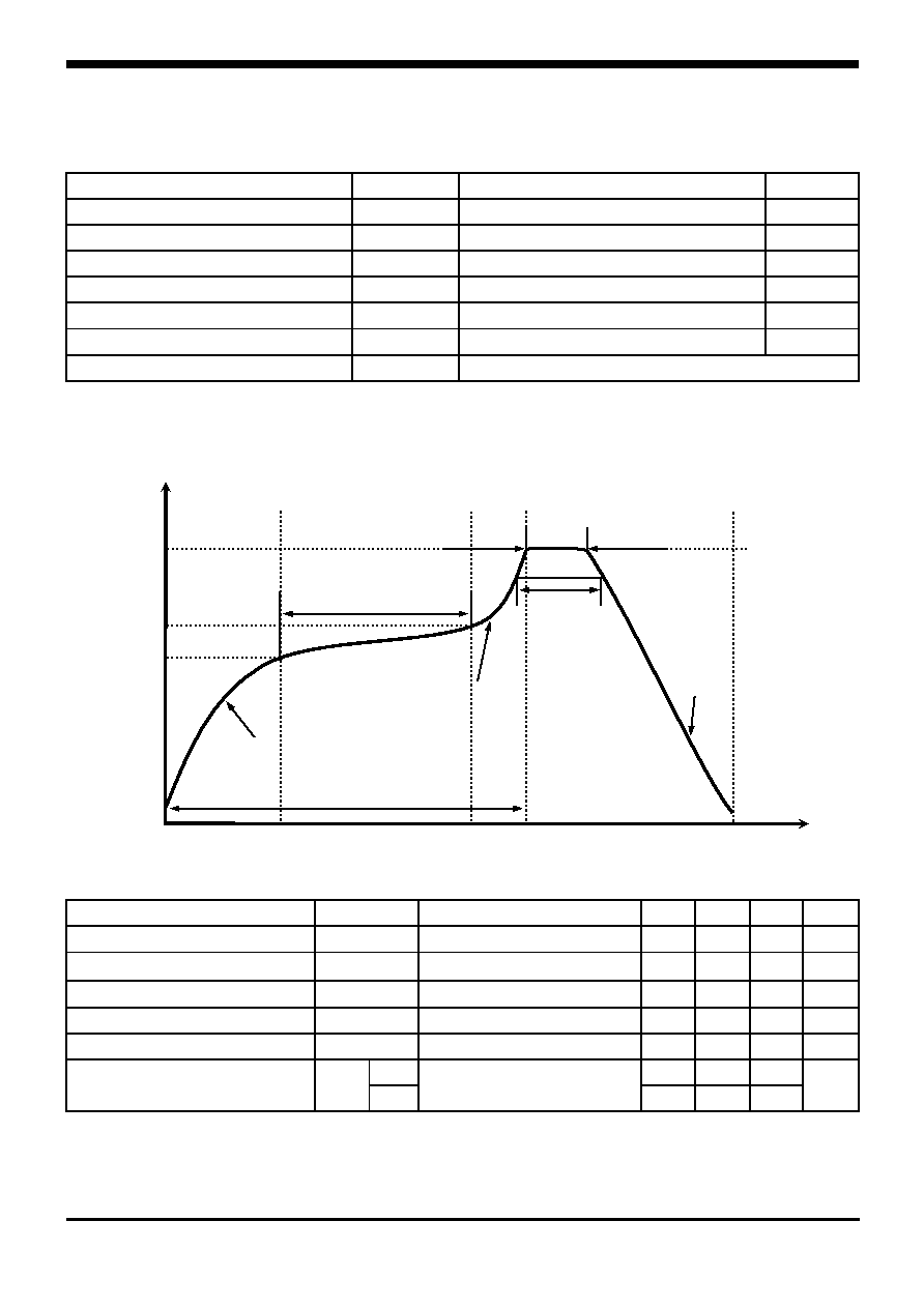
*1. Duty ratio = 1/16, Pulse width = 0.1ms
*2. Recommended reflow soldering temperature profile
- Preheating 150 to 185 within 120 seconds soldering 240 within 10 seconds
Gradual cooling (Avoid quenching)
Electrical / Optical Characteristics
(Ta=25
o
C)
Characteristic Symbol
Test Condition
Min Typ Max Unit
Forward voltage
V
F
I
F
= 20mA
-
2.1
2.5
V
*
3
Luminous intensity
I
V
I
F
= 20mA
68
-
230
mcd
Peak wavelength
P
I
F
= 20mA
-
630
-
nm
Spectrum bandwidth
I
F
= 20mA
-
35
-
nm
Reverse current
I
R
V
R
=4V -
-
10
uA
X
-
±65
-
*
4
Half angle
1/2
Y
I
F
= 20mA
-
±70
-
deg
max. 10sec
Temp ()
Time (sec)
185
150
240
Peak Temp max. 240
Preheating area
150~185, 90±30sec
max. 3/sec
25
Time from 25 to Peak Temperature max. 6min
Solder area
220, max. 60sec
max. 4/sec
max. -6/sec
240
180
150
60
0

KSD-O8G008-001
3
SA1316-E
*4.
1/2
is the off-axis angle where the luminous intensity is
1/2
the peak intensity
*3. Luminous intensity maximum tolerance for each grade classification limit is ±18%
*3. Luminous Intensity Classification
K L M
68~100 100~155 155~230

KSD-O8G008-001
4
SA1316-E
Fig.4 Spectrum Distribution
Fig. 3 I
F
≠ Ta
Fig. 2 I
V
- I
F
Fig. 1 I
F
- V
F
Electrical Characteristic Curves
Fig. 5-1 Radiation Diagram(X)
Fig. 5-2 Radiation Diagram(Y)
F
o
rward Current
I
F
[mA]
Ambient Temperature Ta []
R
e
lative Int
e
nsit
y
[%]
Wavelength [nm]
Forward Voltage V
F
[V]
F
o
rward Current
I
F
[mA]
Forward Current I
F
[mA]
Luminous Intensit
y I
v
[mc
d
]
Relative Luminous Intensity Iv [%]
Relative Luminous Intensity Iv [%]

KSD-O8G008-001
5
SA1316-E
The AUK Corp. products are intended for the use as components in general electronic
equipment (Office and communication equipment, measuring equipment, home
appliance, etc.).
Please make sure that you consult with us before you use these AUK Corp. products
in equipments which require high quality and / or reliability, and in equipments which
could have major impact to the welfare of human life(atomic energy control, airplane,
spaceship, transportation, combustion control, all types of safety device, etc.). AUK
Corp. cannot accept liability to any damage which may occur in case these AUK Corp.
products were used in the mentioned equipments without prior consultation with AUK
Corp..
Specifications mentioned in this publication are subject to change without notice.