KSD-O2U001-001
1
SAW5670
Dual Color LED Lamp
Features
∑ Milky diffusion lens type
∑ 5mm(T-13/4) all plastic mold type
∑ Radiation color (Amber, White)
∑ Low power consumption
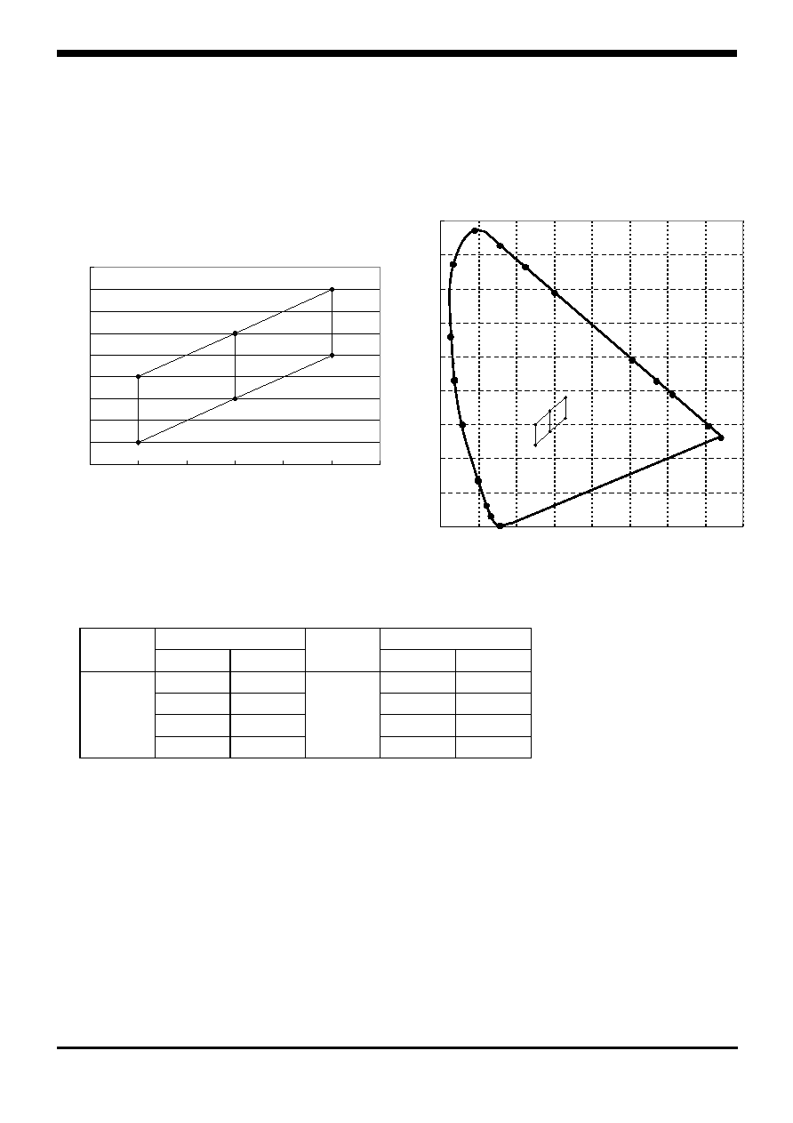
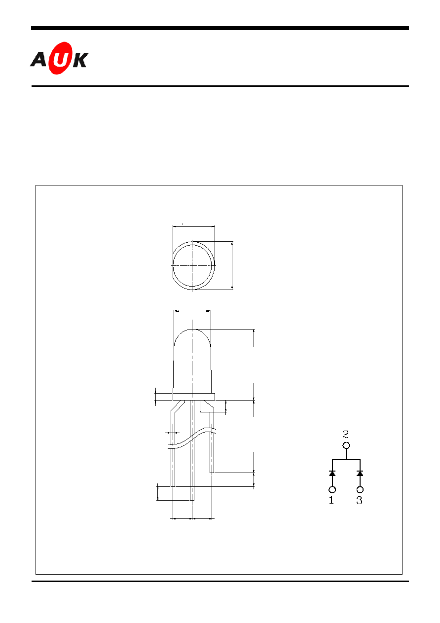
Outline Dimensions unit :
mm
S
S
e
e
m
m
i
i
c
c
o
o
n
n
d
d
u
u
c
c
t
t
o
o
r
r
PIN Connections
1. Anode (White)
2. Common Cathode
3. Anode (Amber)
2.54 Typ.
2.54 Typ.
0
.
6
0
~
1
.
0
0
0 . 4 0 ~ 0 . 6 0
0
.
2
0
~
0
.
8
0
M
i
n
2
6
.
0
0
M
i
n
2
6
.
0
0
8
.
4
0
~
8
.
8
0
ÿ4.60~5.00
5
.
6
0
~
6
.
0
0
5 20~5.60
1 2 3
KSD-O2U001-001
2
SAW5670
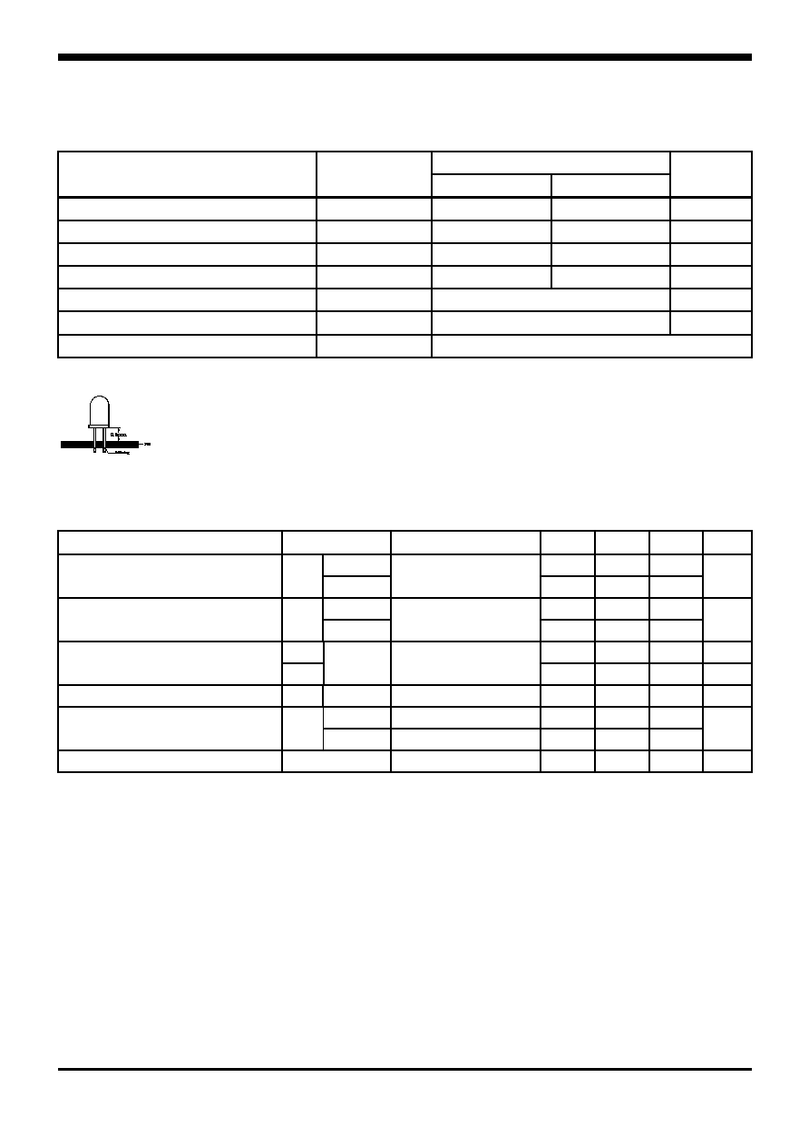
Absolute Maximum Ratings
(Ta=25
o
C)
Rating
Characteristic Symbol
White Amber
Unit
Power dissipation
P
D
125 75
mW
Forward current
I
F
30 30
mA
*
1
Peak forward current
I
FP
50 50
mA
Reverse voltage
V
R
10 16
V
Operating temperature range
T
opr
-25 85
Storage temperature range
T
stg
-30 100
*
2
Soldering temperature
T
sol
260
for
10 seconds
*1.Duty ratio = 1/16, Pulse width = 0.1ms
*2.Keep the distance more than 2.0mm from PCB to the bottom of LED package
Electrical / Optical Characteristics
(Ta=25
o
C)
Characteristic Symbol
Test
Condition
Min.
Typ.
Max.
Unit
White -
3.5
4.2
Forward voltage
V
F
Amber
I
F
= 20mA
- 2.0
2.5
V
White -
200
-
Luminous intensity
I
V
Amber
I
F
= 20mA
- 100 -
mcd
X 0.25
-
0.33
-
*
4
Chromaticity coordinates
Y
White I
F
= 20mA
0.24 - 0.38 -
Peak wavelength
P
Amber I
F
= 20mA
-
630
-
nm
White V
R
=10V -
-
10
Reverse current
I
R
Amber V
R
=16V -
-
10
uA
*
3
Half angle
1/2
I
F
= 20mA
-
±20
- deg
*3.
1/2
is the off-axis angle where the luminous intensity is 1/2 the peak intensity
KSD-O2U001-001
3
SAW5670
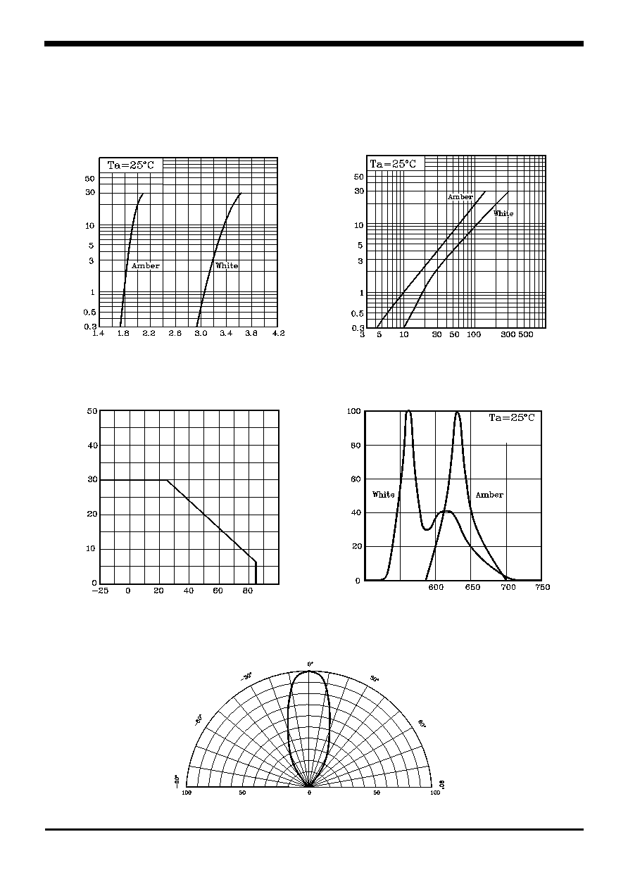
Characteristic Diagrams
Fig. 5 Radiation Diagram
Relative Luminous Intensity Iv [%]
Fig.4 Spectrum Distribution
Fig. 3 I
F
≠ Ta
Fig. 2 I
V
- I
F
Forward Voltage V
F
[V]
F
o
rward Current
I
F
[mA]
Luminous Intensity I
V
[mcd]
F
o
rward Current I
F
[mA]
Fig. 3 I
F
≠ Ta
F
o
rward Current
I
F
[mA]
Ambient Temperature Ta [
]
R
e
lative Int
e
nsit
y
[%]
Wavelength [nm]
Fig. 1 I
F
- V
F
Fig.4 Spectrum Distribution
400
450 ...
I
F
=20mA
KSD-O2U001-001
5
SAW5670
The AUK Corp. products are intended for the use as components in general electronic
equipment (Office and communication equipment, measuring equipment, home
appliance, etc.).
Please make sure that you consult with us before you use these AUK Corp. products
in equipments which require high quality and / or reliability, and in equipments which
could have major impact to the welfare of human life(atomic energy control, airplane,
spaceship, transportation, combustion control, all types of safety device, etc.). AUK
Corp. cannot accept liability to any damage which may occur in case these AUK Corp.
products were used in the mentioned equipments without prior consultation with AUK
Corp..
Specifications mentioned in this publication are subject to change without notice.