
SRAM
MT5C6404
Austin Semiconductor, Inc.
MT5C6404
Rev. 1.0 9/01
Austin Semiconductor, Inc. reserves the right to change products or specifications without notice.
1
FEATURES
∑ Speeds: 12, 15, 20, 25, 35, 45, 55, and 70ns
∑ Battery Backup: 2V data retention
∑ High-performance, low-power CMOS double-metal
process
∑ Single +5V (+10%) Power Supply
∑ Easy memory expansion with CE\
∑ All inputs and outputs are TTL compatible
OPTIONS
MARKING
∑ Timing
12ns access
-12
15ns access
-15
20ns access
-20
25ns access
-25
35ns access
-35
45ns access
-45*
55ns access
-55*
70ns access
-70*
∑ Package(s)
Ceramic DIP (300 mil)
C
No. 105
∑ Operating Temperature Ranges
Industrial (-40
o
C to +85
o
C)
IT
Military (-55
o
C to +125
o
C)
XT
∑ 2V data retention/low power
L
*Electrical characteristics identical to those provided for the 35ns
access devices.
PIN ASSIGNMENT
(Top View)
AVAILABLE AS MILITARY
SPECIFICATIONS
∑ SMD 5962-86859
∑ SMD 5962-89692
∑ MIL-STD-883
GENERAL DESCRIPTION
The Austin Semiconductor SRAM family employs
high-speed, low-power CMOS designs using a four-transistor
memory cell. Austin Semiconductor SRAMs are fabricated
using double-layer metal, double-layer polysilicon
technology.
For flexibility in high-speed memory applications, Austin
Semiconductor offers chip enable (CE\) on all organizations.
This enhancement can place the outputs in High-Z for
additional flexibility in system design.
Writing to these devices is accomplished when write
enable (WE\) and CE\ inputs are both LOW. Reading is
accomplished when WE\ remains HIGH and CE\ goes LOW.
The device offers a reduced power standby mode when
disabled. This allows system designs to achieve low standby
power requirements.
All devices operate from a single +5V power supply and
all inputs and outputs are fully TTL compatible.
16K x 4 SRAM
SRAM MEMORY ARRAY
For more products and information
please visit our web site at
www.austinsemiconductor.com
22-Pin DIP (C)
(300 MIL)
1
2
3
4
5
6
7
8
9
10
11
22
21
20
19
18
17
16
15
14
13
12
A5
A6
A7
A8
A9
A10
A11
A12
A13
CE\
Vss
Vcc
A4
A3
A2
A1
A0
DQ4
DQ3
DQ2
DQ1
WE\
SRAM
MT5C6404
Austin Semiconductor, Inc.
MT5C6404
Rev. 1.0 9/01
Austin Semiconductor, Inc. reserves the right to change products or specifications without notice.
2
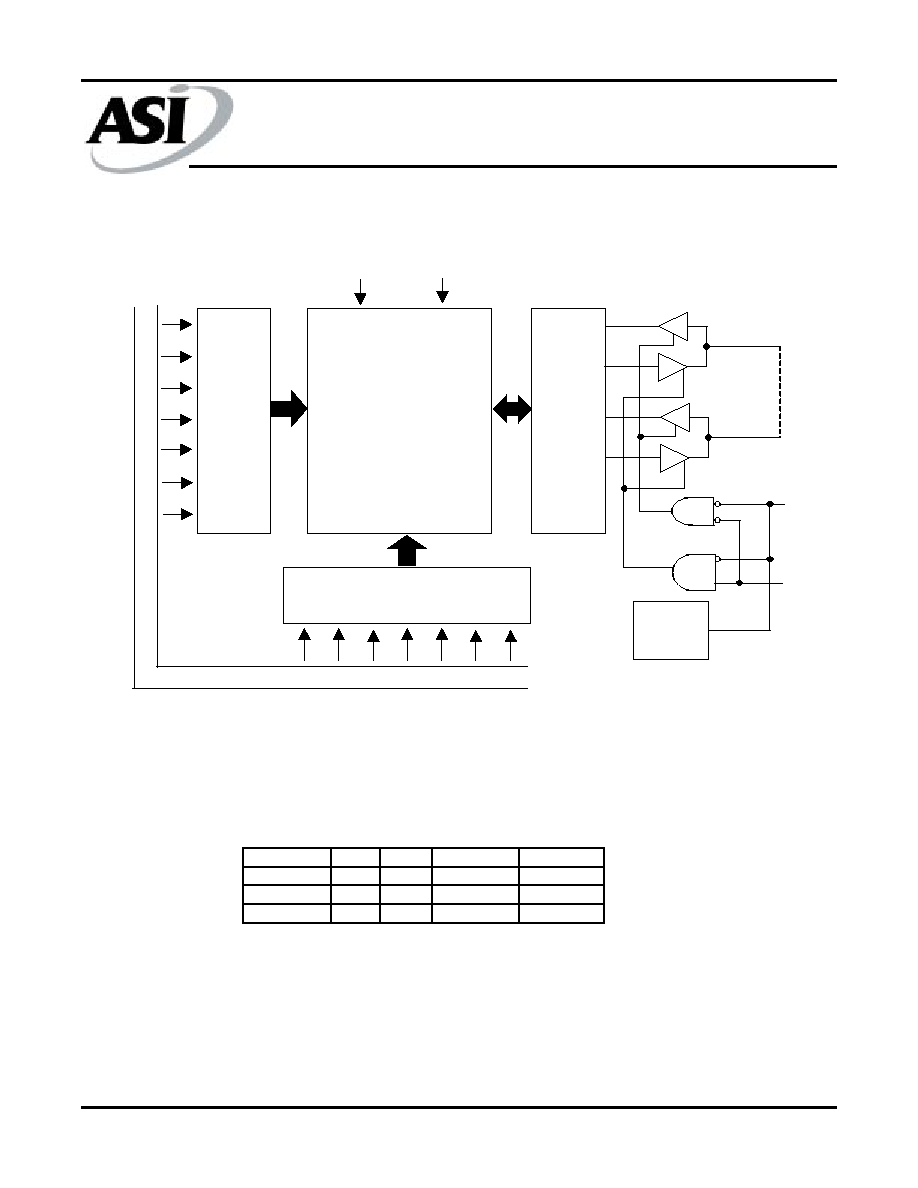
FUNCTIONAL BLOCK DIAGRAM
TRUTH TABLE
ROW DECODER
65,536-BIT
MEMORY ARRAY
I/O CONTROL
V
CC
GND
DQ4
WE\
A
A
A
A
A
A
A
COLUMN DECODER
A A A A A A A
POWER
DOWN
CE\
(LSB)
(LSB)
DQ
DIP
MODE
CE\
WE\
DQ
POWER
STANDBY
H
X
HIGH-Z
STANDBY
READ
L
H
Q
ACTIVE
WRITE
L
L
D
ACTIVE
SRAM
MT5C6404
Austin Semiconductor, Inc.
MT5C6404
Rev. 1.0 9/01
Austin Semiconductor, Inc. reserves the right to change products or specifications without notice.
3
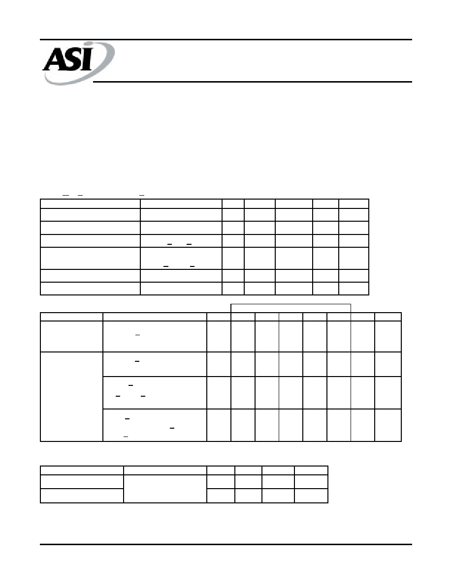
ABSOLUTE MAXIMUM RATINGS*
Voltage on any Input or DQ Relative to Vss...-2.0V to +7.0V
Voltage on Vcc Supply Relative to Vss...........-1.0V to +7.0V
Storage Temperature.....................................-65
o
C to +150
o
C
Power Dissipation.................................................................1W
Max Junction Temperature............................................+175
∞
C
Lead Temperature (soldering 10 seconds)...................+260
o
C
Short Circuit Output Current...........................................50mA
*Stresses greater than those listed under "Absolute Maximum
Ratings" may cause permanent damage to the device. This is
a stress rating only and functional operation of the device at
these or any other conditions above those indicated in the
operation section of this specification is not implied. Exposure
to absolute maximum rating conditions for extended periods
may affect reliability.
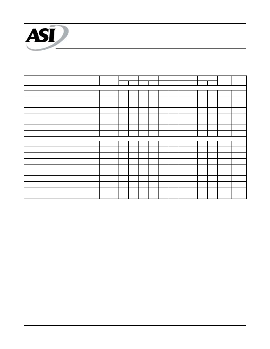
ELECTRICAL CHARACTERISTICS AND RECOMMENDED DC OPERATING CONDITIONS
(-55
o
C < T
C
< 125
o
C; V
CC
= 5V +10%)
CAPACITANCE
DESCRIPTION
CONDITIONS
SYM
MIN
MAX
UNITS NOTES
Input High (Logic 1) Voltage
V
IH
2.2
Vcc+1.0V
V
1
Input Low (Logic 0) Voltage
V
IL
-0.5
0.8
V
1, 2
Input Leakage Current
0V < V
IN
< V
CC
IL
I
-10
10
µA
Output Leakage Current
Outputs Disabled
0V < V
OUT
< V
CC
IL
O
-10
10
µA
Output High Voltage
I
OH
= -4.0mA
V
OH
2.4
---
V
1
Output Low Voltage
I
OL
= 8.0mA
V
OL
---
0.4
V
1
SYM
-12
-15
-20
-25
-35
UNITS NOTES
I
cc
140
125
110
100
90
mA
3
Power Supply
Current: Standby
I
SBT1
45
41
36
33
30
mA
I
SBT2
25
25
25
25
25
mA
I
SBC2
5
5
5
5
5
mA
Power Supply
Current: Operating
PARAMETER
CE\ > (V
CC
-0.2); V
CC
= MAX
All Other Inputs < 0.2V
or > (V
CC
- 0.2V), f = 0 Hz
CE\ > V
IH
; V
CC
= MAX
f = 1/t
RC
(MIN) Hz
MAX
CONDITIONS
CE\ < V
IL
; V
CC
= MAX
Output Open
CE\ > V
IH
; All Other Inputs
< V
IL
or > V
IH
, V
CC
= MAX
f = 0 Hz
DESCRIPTION
CONDITIONS
SYM
MAX
UNITS
NOTES
Input Capacitance
C
I
6
pF
4
Output Capacitance
C
O
7
pF
4
T
A
= 25
o
C, f = 1MHz
Vcc = 5V
SRAM
MT5C6404
Austin Semiconductor, Inc.
MT5C6404
Rev. 1.0 9/01
Austin Semiconductor, Inc. reserves the right to change products or specifications without notice.
4
ELECTRICAL CHARACTERISTICS AND RECOMMENDED AC OPERATING CONDITIONS
(Note 5) (-55
o
C < T
C
< 125
o
C; V
CC
= 5V +10%)
MIN MAX MIN MAX MIN MAX MIN MAX MIN MAX
READ CYCLE
READ cycle time
t
RC
12
15
20
25
35
ns
Address access time
t
AA
12
15
20
25
35
ns
Chip Enable access time
t
ACE
10
13
15
20
25
ns
Output hold from address change
t
OH
2
2
2
2
2
ns
Chip Enable to output in Low-Z
t
LZCE
2
2
2
2
2
ns
7
Chip disable to output in High-Z
t
HZCE
7
8
10
12
15
ns
6, 7
Chip Enable to power-up time
t
PU
0
0
0
0
0
ns
Chip disable to power-down time
t
PD
12
15
20
25
35
ns
WRITE CYCLE
WRITE cycle time
t
WC
12
15
20
25
35
ns
Chip Enable to end of write
t
CW
10
12
15
20
25
ns
Address valid to end of write
t
AW
10
12
15
20
25
ns
Address setup time
t
AS
0
0
0
0
0
ns
Address hold from end of write
t
AH
0
0
0
0
0
ns
WRITE pulse width
t
WP
10
12
15
20
25
ns
Data setup time
t
DS
7
8
10
12
15
ns
Data hold time
t
DH
0
0
0
0
0
ns
Write disable to output in Low-Z
t
LZWE
2
2
2
2
2
ns
7
Write Enable to output in High-Z
t
HZWE
0
6
0
7
0
8
0
10
0
15
ns
6, 7
NOTES
DESCRIPTION
-12
SYMBOL
UNITS
-35
-25
-20
-15

SRAM
MT5C6404
Austin Semiconductor, Inc.
MT5C6404
Rev. 1.0 9/01
Austin Semiconductor, Inc. reserves the right to change products or specifications without notice.
5
AC TEST CONDITIONS
Input pulse levels ...................................... Vss to 3.0V
Input rise and fall times ......................................... 5ns
Input timing reference levels ................................ 1.5V
Output reference levels ....................................... 1.5V
Output load ................................. See Figures 1 and 2
NOTES
1.
All voltages referenced to V
SS
(GND).
2.
-3V for pulse width < 20ns
3.
I
CC
is dependent on output loading and cycle rates.
The specified value applies with the outputs
unloaded, and f = 1 Hz.
t
RC (MIN)
4.
This parameter is sampled.
5.
Test conditions as specified with the output loading
as shown in Fig. 1 unless otherwise noted.
6.
t
HZCE
and t
HZWE
are specified with CL = 5pF as in
Fig. 2. Transition is measured ±500mV typical from steady
state voltage, allowing for actual tester RC time constant.
7.
At any given temperature and voltage condition,
t
HZCE
is less than t
LZCE
, and t
HZWE
is less than t
LZWE
.
8.
WE\ is HIGH for READ cycle.
9.
Device is continuously selected. Chip enable is held in
its active state.
10. Address valid prior to, or coincident with, latest
occurring chip enable.
11.
t
RC = READ Cycle Time.
12. Chip enable (CE\) and write enable (WE\) can initiate
and terminate a WRITE cycle.
Fig. 1 Output Load
Equivalent
Fig. 2 Output Load
Equivalent
DATA RETENTION ELECTRICAL CHARACTERISTICS (L Version Only)
123
123
123
123
1234
1234
1234
1234
DON'T CARE
UNDEFINED
LOW Vcc DATA RETENTION WAVEFORM
12345678
12345678
12345678
12345678
123
123
123
123
1234
1234
1234
1234
123456789
123456789
123456789
123456789
123
123
123
123
1234
1234
1234
1234
DATA RETENTION MODE
V
DR
> 2V
4.5V
4.5V
V
DR
t
CDR
t
R
V
IH
V
IL
V
CC
CE\
DESCRIPTION
SYM
MIN
MAX
UNITS
NOTES
V
CC
for Retention Data
V
DR
2
---
V
V
CC
= 2V
I
CCDR
---
300
µA
V
CC
= 3V
I
CCDR
---
500
µA
Chip Deselect to Data
Retention Time
t
CDR
0
---
ns
4
Operation Recovery Time
t
R
t
RC
---
ns
4, 11
CONDITIONS
Data Retention Current
CE\ > (V
CC
- 0.2V)
V
IN
> (V
CC
- 0.2V)
or < 0.2V
5 pF
+5V
Q
255
480
+5V
Q
255
30pF
480