
AL5DS9xx9V
©2002-Copyright by AverLogic Technologies, Corp.
Preliminary Version 0.6
1
AL5DS9xx9V Data Sheets
3.3V Synchronous Dual-Port SRAM
AL5DS9349V/59V/69V/79V
4K/8K/16K/32K x 18 bits
AL5DS9269/79V
16K/32K x 16 bits
AL5DS9149/59/69/79/89V
4K/8K/16K/32K/64K x 9 bits
AL5DS9069/79/89V
16K/32K/64K x 8 bits
Preliminary

AL5DS9xx9V
©2002-Copyright by AverLogic Technologies, Corp.
Preliminary Version 0.6
2
Amendments
(Since January 4, 2002)
02.01.04 Preliminary
version
0.1
02.01.10
Preliminary version 0.2:
(1) Modifies truth table and note descriptions in paragraph 7
(2) Modifies Absolute Maximum Ratings in paragraph 8.1
(3) Modifies C
IN
and C
OUT
DC characteristics in paragraph 8.3
(4) Modifies Bank Select Pipelined Read and Counter Rest in Pipelined Mode timing
diagrams
02.04.09
Preliminary version 0.3:
(1) Modifies features in paragraph 2
(2) Modifies ordering information in paragraph 4.1
(3) Modifies AC characteristics in paragraph 8.5
02.05.07
Preliminary version 0.4:
(1) Modifies marking information in paragraphs 4 and 6
(2) Modifies the font type in paragraphs 6 and 9
02.09.25
Preliminary version 0.5:
(1) Split the datasheets to two parts: AL5DS9389V/9289V/9199V/9099V for 1M bit
density and other parts for less than 1M bit density
(2) Modifies the pin-out diagram in paragraph 6
(3) Modifies the truth table of address control in paragraph 7
02.11.01
Preliminary version 0.6:
Modifies the DC characteristics in paragraph 8.3
THE INFORMATION CONTAINED HEREIN IS SUBJECT TO CHANGE WIHOUT NOTICE.

AL5DS9xx9V
©2002-Copyright by AverLogic Technologies, Corp.
Preliminary Version 0.6
3
AL5DS9XX9V 3.3V Synchronous Dual-Port SRAM
Contents:
1
General Description ...............................................................................................4
2
Features ..................................................................................................................4
3
Applications ............................................................................................................5
4
Chip Information....................................................................................................5
4.1 Marking Information.............................................................................................................5
4.2 Ordering Information............................................................................................................5
5
Function Block Diagram .......................................................................................7
6
Pin-out Diagram.....................................................................................................8
7
Pin Definition and Description..............................................................................9
8
Electrical Characteristics.....................................................................................16
8.1 Absolute Maximum Ratings................................................................................................16
8.2 Recommended Operating Conditions ................................................................................16
8.3 DC Characteristics ...............................................................................................................17
8.4 AC Test Loads ......................................................................................................................18
8.5 AC Characteristics ...............................................................................................................18
9
Timing Diagrams .................................................................................................21
10 Mechanical Drawing ............................................................................................27

AL5DS9xx9V
©2002-Copyright by AverLogic Technologies, Corp.
Preliminary Version 0.6
4
1 General Description
A Dual-port RAM is a static RAM with a dual-ported cell. There are separate address, data and
control signals for each port to access a common SRAM array. A dual-port RAM is generally
classified with FIFOs as a "specialty" memory. They are most commonly used in communications
that include the exchange of data between processors, processes and systems.
Each port contains an internal counter for fast memory access applications. The initial address of the
internal counter is loaded with the port's Address Strobe (/ADS). It also allows the Counter Enable
(/CNTEN) to increment the internal counter on each Low to High transition of that port's clock
signal. The counter can address the entire memory array and will loop back to start (address 0). The
internal counter will be reset to zero while asserting Counter Reset (/CNTRST).
The AL5DS9xx9V is a high speed, 3.3V, synchronous, CMOS, dual-ported SRAM series. The
AL5DS9389V is configured as 64K x 18-bit, AL5DS9289V as 64K x 16-bit, AL5DS9199V as
128K x 9-bit and AL5DS9099V as 128K x 8-bit. All these parts support both Pipelined and Flow-
Through modes that are selected via the Pipe/FT pin. In the Pipelined mode, two cycles are required
to reactivate the data outputs. The AL5DS9xx9V series features dual Chip Enables that allow
simple depth and width expansion without external control logic.
All parts are available in 100-pin Thin Quad Plastic Flatpack (TQFP) packages. AL5DS9289V and
AL5DS9389V are also available in 128-pin TQFP packages.
2 Features
True dual ported memory cells
4 Flow-Through/Pipelined devices:
-- 64K x 18-bit organization (AL5DS9389V)
-- 64K x 16-bit organization (AL5DS9289V)
-- 128K x 9-bit organization (AL5DS9199V)
-- 128K x 8-bit organization (AL5DS9099V)
Supports byte write/read for 16/18 bit devices
Separate upper-byte and lower-byte controls for bus matching (only for 16/18 bit devices)
3 modes supported:
-Pipelined
-Flow-Through
-Burst
Counter enable and reset
Fast 100-MHz operation on both ports in Pipelined output mode
Supports depth and width expansion
0.25-micron CMOS for optimum speed/power
High speed clock to data access
3.3V low operating power
Pin-compatible and functionally equivalent to IDT or Cypress
Available in 100 or 128 pin TQFP

AL5DS9xx9V
©2002-Copyright by AverLogic Technologies, Corp.
Preliminary Version 0.6
5
3 Applications
Cellular Base Stations
Cellular Phones
Multi-protocol Routers
LAN/WAN Switches
PBXs
RAIDs (Storage Networks)
Set-top Boxes
Audio/Video Editing
Graphics Accelerators
Satellite Encoders
Cable Modems
Flight Simulators
High-end Printing Servers
Ultrasound Imaging
4 Chip Information
4.1 Marking Information
4.2 Ordering Information
Two packages are available for AL5DS9xx9V series Synchronous Dual-Port SRAM.
Part number
Speed
(MHz)
Package Power
Supply
Word
Length
Bus
Width
AL5DS9069V (A-100-PF100)
100
100 pin TQFP
3.3V 10%
16K 8
bits
AL5DS9069V (A-83-PF100)
83
100 pin TQFP
3.3V 10%
16K 8
bits
AL5DS9079V (A-100-PF100)
100
100 pin TQFP
3.3V 10%
32K 8
bits
AL5DS9079V (A-83-PF100)
83
100 pin TQFP
3.3V 10%
32K 8
bits
AL5DS9089V (A-100-PF100)
100
100 pin TQFP
3.3V 10%
64K 8
bits
AL5DS9089V (A-83-PF100)
83
100 pin TQFP
3.3V 10%
64K 8
bits
AL5DS9149V (A-100-PF100)
100
100 pin TQFP
3.3V 10%
4K 9
bits
AL5DS9149V (A-83-PF100)
83
100 pin TQFP
3.3V 10%
4K 9
bits
AL5DS9159V (A-100-PF100)
100
100 pin TQFP
3.3V 10%
8K 9
bits

AL5DS9xx9V
©2002-Copyright by AverLogic Technologies, Corp.
Preliminary Version 0.6
6
Part number
Speed
(MHz)
Package Power
Supply
Word
Length
Bus
Width
AL5DS9159V (A-83-PF100)
83
100 pin TQFP
3.3V 10%
8K 9
bits
AL5DS9169V (A-100-PF100)
100
100 pin TQFP
3.3V 10%
16K 9
bits
AL5DS9169V (A-83-PF100)
83
100 pin TQFP
3.3V 10%
16K 9
bits
AL5DS9179V (A-100-PF100)
100
100 pin TQFP
3.3V 10%
32K 9
bits
AL5DS9179V (A-83-PF100)
83
100 pin TQFP
3.3V 10%
32K 9
bits
AL5DS9189V (A-100-PF100)
100
100 pin TQFP
3.3V 10%
64K 9
bits
AL5DS9189V (A-83-PF100)
83
100 pin TQFP
3.3V 10%
64K 9
bits
AL5DS9269V (A-100-PF100)
100
100 pin TQFP
3.3V 10%
16K 16
bits
AL5DS9269V (A-83-PF100)
83
100 pin TQFP
3.3V 10%
16K 16
bits
AL5DS9279V (A-100-PF100)
100
100 pin TQFP
3.3V 10%
32K 16
bits
AL5DS9279V (A-83-PF100)
83
100 pin TQFP
3.3V 10%
32K 16
bits
AL5DS9269V (A-100-PF128)
100
128 pin TQFP
3.3V 10%
16K 16
bits
AL5DS9269V (A-83-PF128)
83
128 pin TQFP
3.3V 10%
16K 16
bits
AL5DS9279V (A-100-PF128)
100
128 pin TQFP
3.3V 10%
32K 16
bits
AL5DS9279V (A-83-PF128)
83
128 pin TQFP
3.3V 10%
32K 16
bits
AL5DS9349V (A-100-PF100)
100
100 pin TQFP
3.3V 10%
4K 18
bits
AL5DS9349V (A-83-PF100)
83
100 pin TQFP
3.3V 10%
4K 18
bits
AL5DS9359V (A-100-PF100)
100
100 pin TQFP
3.3V 10%
8K 18
bits
AL5DS9359V (A-83-PF100)
83
100 pin TQFP
3.3V 10%
8K 18
bits
AL5DS9369V (A-100-PF100)
100
100 pin TQFP
3.3V 10%
16K 18
bits
AL5DS9369V (A-83-PF100)
83
100 pin TQFP
3.3V 10%
16K 18
bits
AL5DS9379V (A-100-PF100)
100
100 pin TQFP
3.3V 10%
32K 18
bits
AL5DS9379V (A-83-PF100)
83
100 pin TQFP
3.3V 10%
32K 18
bits
AL5DS9379V (A-100-PF128)
100
128 pin TQFP
3.3V 10%
32K 18
bits
AL5DS9379V (A-83-PF128)
83
128 pin TQFP
3.3V 10%
32K 18
bits

AL5DS9xx9V
©2002-Copyright by AverLogic Technologies, Corp.
Preliminary Version 0.6
7
5 Function Block Diagram
AL5DS9xx9V
©2002-Copyright by AverLogic Technologies, Corp.
Preliminary Version 0.6
8
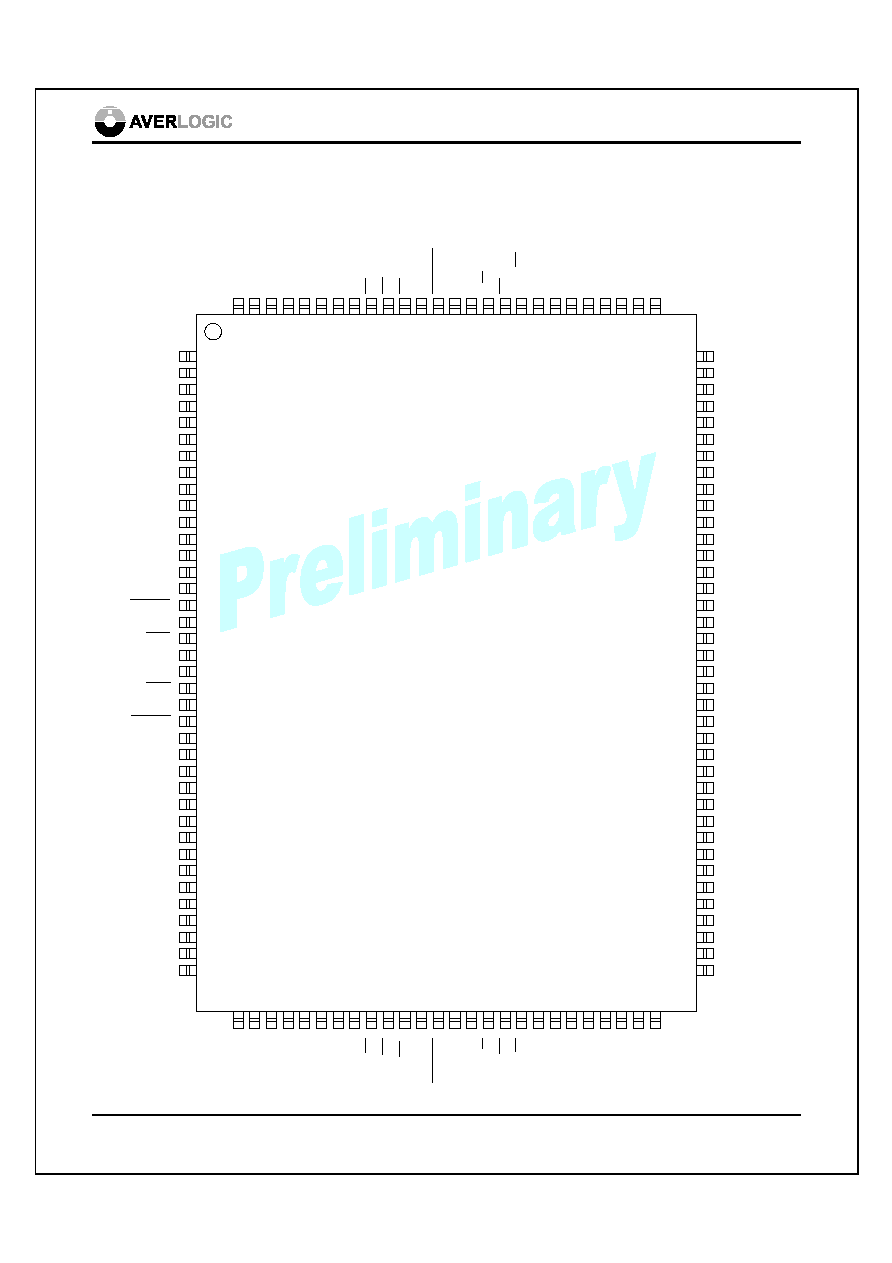
6 Pin-out Diagram
128 pin 14mm*20mm*1.4mm TQFP package-1:

AL5DS9xx9V
©2002-Copyright by AverLogic Technologies, Corp.
Preliminary Version 0.6
9
128 pin 14mm*20mm*1.4mm TQFP package-2:

AL5DS9xx9V
©2002-Copyright by AverLogic Technologies, Corp.
Preliminary Version 0.6
10
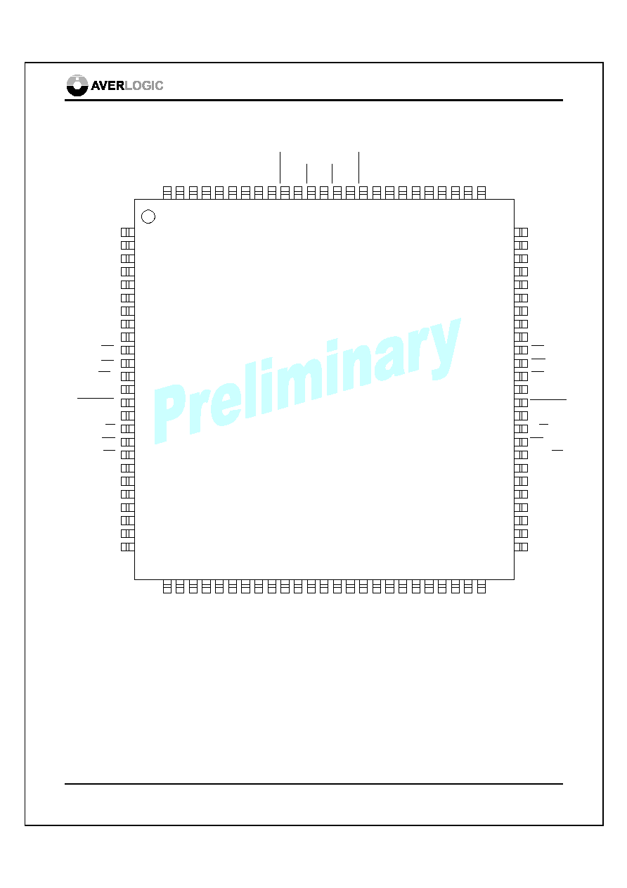
100 pin 14mm*14mm*1.4mm TQFP package-1:
100-Pin TQFP (Top View)
AL5DS9379V(A-100-PF100): 32K * 18
AL5DS9379V(A-83-PF100): 32K * 18
AL5DS9369V(A-100-PF100): 16K * 18
AL5DS9369V(A-83-PF100): 16K * 18
AL5DS9359V(A-100-PF100): 8K * 18
AL5DS9359V(A-83-PF100): 8K * 18
AL5DS9349V(A-100-PF100): 4K * 18
AL5DS9349V(A-83-PF100): 4K * 18
Note 1: pins 6 and 69 are NC for AL5DS9369V/59V/49V
Note 2: pins 5 and 70 are NC for AL5DS9359V/49V
Note 3: pins 4 and 71 are NC for AL5DS9349V
GND
GND
A
8L
A
3L
A
4L
A
5L
A
6L
A
7L
A
0L
A
1L
A
2L
ADS
L
CL
K
L
CN
T
E
N
L
ADS
R
CL
K
R
CN
T
E
N
R
A
0R
A
3R
A
4R
A
5R
A
1R
A
2R
A
6R
A
7R
GN
D
GN
D
V
CC
I/O
9L
I/O
8L
I/O
7L
I/O
6L
I/O
3L
I/O
2L
I/O
1L
I/O
0L
I/O
5L
I/O
4L
V
CC
I/
O
1R
I/
O
0R
I/
O
3R
I/
O
2R
I/
O
5R
I/
O
4R
I/
O
7R
I/
O
6R
I/
O
9R
I/
O
8R
I/O
10
R
72
73
74
75
68
69
70
71
64
65
66
67
60
61
62
63
56
57
58
59
52
53
54
55
51
76
77
78
79
80
81
82
83
84
85
86
87
88
89
90
91
92
93
94
95
96
97
98
99
10
0
1
11
10
9
8
7
6
5
4
3
2
25
24
23
22
21
20
19
18
17
16
15
14
13
12
39
40
44
43
42
41
50
45
49
48
47
46
26
27
31
30
29
28
37
32
36
35
34
33
38
GND
GND
I/O
11R
PIPE/FT
R
OE
R
R/W
R
I/O
16R
I/O
15R
I/O
14R
I/O
13R
I/O
12R
I/O
17R
LB
R
UB
R
CE
0R
CE
1R
CNTRST
R
A
9R
A
10R
A
11R
A
14R
[NC]
A
8R
A
13R
[NC]
NC
A
12R
[NC]
A
9L
A
10L
A
11L
[NC]A
12L
[NC]A
13L
[NC]A
14L
GND
I/O
16L
LB
L
UB
L
CE
0L
CE
1L
CNTRST
L
V
CC
R/W
L
OE
L
PIPE/FT
L
I/O
17L
NC
I/O
14L
I/O
15L
I/O
12L
I/O
13L
I/O
10L
I/O
11L
AL5DS9xx9V
©2002-Copyright by AverLogic Technologies, Corp.
Preliminary Version 0.6
11
100 pin 14mm*14mm*1.4mm TQFP package-2:
100-Pin TQFP (Top View)
AL5DS9279V(A-100-PF100): 32K * 16
AL5DS9279V(A-83-PF100): 32K * 16
AL5DS9269V(A-100-PF100): 16K * 16
AL5DS9269V(A-83-PF100): 16K * 16
Note 1: pins 6 and 70 are NC for AL5DS9269V
A
9L
A
10L
A
11L
A
12L
A
13L
[NC]A
14L
GND
LB
L
NC
CE
0L
CE
1L
CNTRST
L
V
CC
R/W
L
OE
L
PIPE/FT
L
NC
I/O
14L
I/O
15L
I/O
12L
I/O
13L
I/O
10L
I/O
11L
GND
GND
I/O
11R
PIPE/FT
R
OE
R
R/W
R
I/O
15R
I/O
14R
I/O
13R
I/O
12R
LB
R
UB
R
CE
0R
CE
1R
CNTRST
R
A
9R
A
10R
A
11R
A
12R
A
13R
A
14R
[NC]
GND
A
8L
A
3L
A
4L
A
5L
A
6L
A
7L
A
0L
A
1L
A
2L
ADS
L
CL
K
L
CN
T
E
N
L
ADS
R
CL
K
R
CN
T
E
N
R
A
0R
A
3R
A
4R
A
5R
A
1R
A
2R
A
6R
A
7R
GN
D
GN
D
V
CC
I/O
9L
I/O
8L
I/O
7L
I/O
6L
I/O
3L
I/O
2L
I/O
1L
I/O
0L
I/O
5L
I/O
4L
V
CC
I/
O
1R
I/
O
0R
I/
O
3R
I/
O
2R
I/
O
5R
I/
O
4R
I/
O
7R
I/
O
6R
I/
O
9R
I/
O
8R
NC
72
73
74
75
68
69
70
71
64
65
66
67
60
61
62
63
56
57
58
59
52
53
54
55
51
76
77
78
79
80
81
82
83
84
85
86
87
88
89
90
91
92
93
94
95
96
97
98
99
10
0
1
11
10
9
8
7
6
5
4
3
2
25
24
23
22
21
20
19
18
17
16
15
14
13
12
39
40
44
43
42
41
50
45
49
48
47
46
26
27
31
30
29
28
37
32
36
35
34
33
38
LB
L
NC
I/O
10R
NC
NC
A
8R
NC

AL5DS9xx9V
©2002-Copyright by AverLogic Technologies, Corp.
Preliminary Version 0.6
12
100 pin 14mm*14mm*1.4mm TQFP package-3:
100-Pin TQFP (Top View)
AL5DS9189V(A-100-PF100): 64K * 9
AL5DS9189V(A-83-PF100): 64K * 9
AL5DS9179V(A-100-PF100): 32K * 9
AL5DS9179V(A-83-PF100): 32K * 9
AL5DS9169V(A-100-PF100): 16K * 9
AL5DS9169V(A-83-PF100): 16K * 9
AL5DS9159V(A-100-PF100): 8K * 9
AL5DS9159V(A-83-PF100): 8K * 9
AL5DS9149V(A-100-PF100): 4K * 9
AL5DS9149V(A-83-PF100): 4K * 9
Note 1: pins 11 and 65 are NC for AL5DS9179V/69V/59V/49V
Note 2: pins 10 and 66 are NC for AL5DS9169V/59V/49V
Note 3: pins 9 and 67 are NC for AL5DS9159V/49V
Note 4: pins 8 and 68 are NC for AL5DS9149V
NC
A
7L
A
8L
[NC]A
12L
[NC]A
13L
[NC]A
14L
NC
NC
CE
0L
CE
1L
CNTRST
L
V
CC
R/W
L
OE
L
PIPE/FT
L
[NC]A
15L
GND
GND
PIPE/FT
R
OE
R
R/W
R
CE
0R
CE
1R
CNTRST
R
A
9R
A
10R
A
11R
A
12R
[NC]
A
13R
[NC]
GN
D
NC
A
3L
A
4L
A
5L
A
6L
NC
A
0L
A
1L
A
2L
AD
S
L
CLK
L
CNT
EN
L
AD
S
R
CLK
R
CNT
EN
R
A
0R
A
3R
A
4R
A
5R
A
1R
A
2R
A
6R
GND
GND
V
CC
GND
I/
O
8L
I/
O
7L
I/
O
6L
I/
O
3L
I/
O
2L
I/
O
1L
I/
O
0L
I/
O
5L
I/
O
4L
V
CC
I/O
1R
I/O
0R
I/O
3R
I/O
2R
I/O
5R
I/O
4R
I/O
7R
I/O
6R
NC
I/O
8R
NC
72
73
74
75
68
69
70
71
64
65
66
67
60
61
62
63
56
57
58
59
52
53
54
55
51
76
77
78
79
80
81
82
83
84
85
86
87
88
89
90
91
92
93
94
95
96
97
98
99
10
0
1
11
10
9
8
7
6
5
4
3
2
25
24
23
22
21
20
19
18
17
16
15
14
13
12
39
40
44
43
42
41
50
45
49
48
47
46
26
27
31
30
29
28
37
32
36
35
34
33
38
NC
NC
NC
GN
D
NC
NC
NC
NC
NC
NC
A
9L
A
10L
A
11L
NC
NC
NC
NC
NC
A
8R
A
7R
A
14R
[NC]
A
15R
[NC]
NC

AL5DS9xx9V
©2002-Copyright by AverLogic Technologies, Corp.
Preliminary Version 0.6
13
100 pin 14mm*14mm*1.4mm TQFP package-4:
100-Pin TQFP (Top View)
AL5DS9089V(A-100-PF100): 64K * 8
AL5DS9089V(A-83-PF100): 64K * 8
AL5DS9079V(A-100-PF100): 32K * 8
AL5DS9079V(A-83-PF100): 32K * 8
AL5DS9069V(A-100-PF100): 16K * 8
AL5DS9069V(A-83-PF100): 16K * 8
Note 1: pins 11 and 65 are NC for AL5DS9079V/69V
Note 2: pins 10 and 66 are NC for AL5DS9069V
NC
A
7L
A
8L
A
12L
A
13L
[NC]A
14L
NC
NC
CE
0L
CE
1L
CNTRST
L
V
CC
R/W
L
OE
L
PIPE/FT
L
[NC]A
15L
GND
GND
PIPE/FT
R
OE
R
R/W
R
CE
0R
CE
1R
CNTRST
R
A
9R
A
10R
A
11R
A
12R
A
13R
GN
D
NC
A
3L
A
4L
A
5L
A
6L
NC
A
0L
A
1L
A
2L
AD
S
L
CLK
L
CNT
EN
L
AD
S
R
CLK
R
CNT
EN
R
A
0R
A
3R
A
4R
A
5R
A
1R
A
2R
A
6R
GND
GND
V
CC
GND
NC
I/
O
7L
I/
O
6L
I/
O
3L
I/
O
2L
I/
O
1L
I/
O
0L
I/
O
5L
I/
O
4L
V
CC
I/O
1R
I/O
0R
I/O
3R
I/O
2R
I/O
5R
I/O
4R
I/O
7R
I/O
6R
NC
NC
NC
72
73
74
75
68
69
70
71
64
65
66
67
60
61
62
63
56
57
58
59
52
53
54
55
51
76
77
78
79
80
81
82
83
84
85
86
87
88
89
90
91
92
93
94
95
96
97
98
99
10
0
1
11
10
9
8
7
6
5
4
3
2
25
24
23
22
21
20
19
18
17
16
15
14
13
12
39
40
44
43
42
41
50
45
49
48
47
46
26
27
31
30
29
28
37
32
36
35
34
33
38
NC
NC
NC
NC
NC
NC
NC
NC
NC
NC
A
9L
A
10L
A
11L
NC
NC
NC
NC
NC
A
8R
A
7R
A
14R
[NC]
A
15R
[NC]
NC
AL5DS9xx9V
©2002-Copyright by AverLogic Technologies, Corp.
Preliminary Version 0.6
14
7 Pin Definition and Description
The pin-out definitions are described as follows:
Left Port
Right Port
I/O
type
Description
A
0L
~A
16L
A
0R
~A
16R
I
Address
bus.
/ADS
L
/ADS
R
I
Address Strobe. Low active. Asserting this signal LOW
while using an external address will access the port. /ADS
is only dependent of /CNTRST control signal.
/CNTEN
L
/CNTEN
R
I
Counter Enable. Low active. When counter is enabled, the
internal address counter increments one on each rising
edge of CLK regardless of Chip Enable and Lower Byte
or Upper Byte Selects.
/CNTRST
L
/CNTRST
R
I
Counter Reset. Low active. Resets the internal address
counter to zero. This signal is independent of all other
control signals.
/CE
0L
, CE
1L
/CE
0R
, CE
1R
I
Chip Enable. Low active for Chip Enable 0 and High
active for Chip Enable 1.
CLK
L
CLK
R
I
Clock
input.
I/O
0L
~I/O
17L
I/O
0R
~I/O
17R
I/O
Data bus.
/LB
L
/LB
R
I
Lower Byte Select. Low active. Enables the read and
write operations to the lower byte (I/O
0
-I/O
8
for 18 bit
devices, I/O
0
-I/O
7
for 16 bit devices) while asserting this
signal Low. Not available for 8/9 bit devices.
/UB
L
/UB
R
I
Upper Byte Select. Low active. Enables the read and write
operations to the upper byte (I/O
9
-I/O
17
for 18 bit devices,
I/O
8
-I/O
15
for 16 bit devices) while asserting this signal
Low. Not available for 8/9 bit devices.
/OE
L
/OE
R
I
Output Enable. Low active. Asynchronous input signal.
R/W
L
R/W
R
I
Read/Write Enable. High active for read operations and
Low active for write operations.
PIPE/FT
L
PIPE/FT
R
I
Pipelined and Flow-Through Mode Select. High active for
Pipelined mode and Low active for Flow-Through mode.
NC -
No
connection
Digital Power
V
CC
DP
Digital
power
GND DP
Digital
ground
Note: For I/O type, I, O, and DP indicate input, output, and digital power respectively.
AL5DS9xx9V
©2002-Copyright by AverLogic Technologies, Corp.
Preliminary Version 0.6
15
For 18 or 16 bit devices, the truth table of read/write and enable control is as follows:
/CE0 CE1 CLK R/W /UB /LB /OE Upper byte Lower byte
Note
X X X X X
X
H High-Z High-Z Outputs
disabled
L H
H
H
L
L
High-Z
Data output Read Lower byte only
L H
H
L
H
L Data output
High-Z
Read Upper byte only
L H
H
L
L
L Data output Data output Read both bytes
L H
L
H
L
X
High-Z
Data input Write to Lower byte
L H
L
L
H X Data input
High-Z
Write to Upper byte
L H
L
L
L
X Data input
Data input Write to both bytes
X X
X
H H X
High-Z
High-Z
Both bytes disabled
H X
X
X X X
High-Z
High-Z
Chip disabled (Note 2)
X L
X
X X X
High-Z
High-Z
Chip disabled (Note 2)
Note 1: H, L, X, and denote V
IH
, V
IL
, Don't Care and Rising-Edge Trigger, respectively.
Note 2: For Pipelined mode, chip is disabled on the following clock cycle if /CE changes state.
For 9 or 8 bit devices, the truth table of read/write and enable control is as follows:
/CE0 CE1 CLK R/W /OE Data I/O
Note
X X X X H High-Z
Outputs
disabled
L H
H
L Data output Read operation
L H
L X Data
input Write
operation
H X
X
X
High-Z
Chip disabled (Note 2)
X L
X
X
High-Z
Chip disabled (Note 2)
Note 1: H, L, X, and denote V
IH
, V
IL
, Don't Care and Rising-Edge Trigger, respectively.
Note 2: For Pipelined mode, chip is disabled on the following clock cycle if /CE changes state.
The truth table of address counter control is as follows:
/CNTRST /ADS /CNTEN CLK
Address
input
Previous
address
Internal
address
Data I/O
Note
L X X
X X 0 Q
0
Reset internal address
counter to 0
H L X
A
n
X A
n
Q
n
Load external address into
internal address counter
H H L
X A
P
A
P+1
Q
P+1
Enable internal address
counter
H H L
X A
max
A
0
Q
0
Enable internal address
counter (Note 4)
H H H
X A
P
A
P
Q
P
Disable internal address
counter
Note 1: H, L, X, and denote V
IH
, V
IL
, Don't Care and Rising-Edge Trigger, respectively.
Note 2: Assuming /CE
0
, /UB, /LB, and /OE = V
IL
and assuming CE
1
and R/W = V
IH
.

AL5DS9xx9V
©2002-Copyright by AverLogic Technologies, Corp.
Preliminary Version 0.6
16
Note 3: Data I/O is configured in Flow-Through mode. For Pipelined mode, the data output will be
delayed by one cycle.
Note 4: Because the internal address counter will be larger than the maximum memory address, it
will not reset the internal address counter to 0 on the next clock cycle when the previous
internal address has encountered the maximum memory address. Therefore, the application
software should remember to load a new address into the internal address counter or to
invoke the /CNTRST signal to reset the internal address counter to 0 if the internal address
has encountered the maximum memory address.
8 Electrical Characteristics
8.1 Absolute Maximum Ratings
(Exceeding the rating can be harmful to product life. These are only user guidelines and are not
tested.)
Parameter
3.3V Rating
Unit
V
CC
Supply Voltage
-0.3 ~ +3.8
V
V
P
Input Pin Voltage
-0.3 ~ +(V
CC
+0.3) V
I
O
Output Current
-20 ~ +20
mA
T
AMB
Ambient Op. Temperature
0 ~ +85
∞C
T
stg
Storage Temperature
-40 ~ +125
∞C
T
VSOL
Vapor
Phase
Soldering
Temperature (15 Sec.)
220 ∞C
8.2 Recommended Operating Conditions
3.3V Rating
Parameter
Min. Typical Max.
Unit
V
CC
Supply
Voltage
+3.0
+3.3
+3.6
V
V
IH
High Level Input Voltage
0.7 V
CC
V
CC
V
V
IL
Low Level Input Voltage
0
0.3 V
CC
V
T
AMB
Ambient Op. Temperature
0
+70
∞C

AL5DS9xx9V
©2002-Copyright by AverLogic Technologies, Corp.
Preliminary Version 0.6
17
8.3 DC Characteristics
(
V
CC
= 3.3V, GND=0V.
T
AMB
= 0 to 70∞C) Note: Some parameters are guaranteed by
design only and are not production tested.
3.3V Rating
Parameter
Min. Typical Max.
Unit
V
IH
Hi-level Input Voltage
0.7 V
CC
- V
CC
V
V
IL
Lo-level Input Voltage
0
0.3 V
CC
V
V
OH
Hi-level Output Voltage (V
CC
=
Min., I
OH
= -4 mA)
2.4 - V
CC
V
V
OL
Lo-level Output Voltage (V
CC
=
Min., I
OH
= +4 mA)
- -
+0.4
V
C
IN
Input Capacitance at V
CC
=3.3V,
T
A
=25∞C and f=1MHz
10
pF
C
OUT
Output Capacitance at V
CC
=3.3V,
T
A
=25∞C and f=1MHz
10
pF
I
LI
Input Leakage Current (V
CC
=
3.6V, V
IN
= 0V~ V
CC
)
+5
A
I
LO
Output Leakage Current (CE
1
=
V
IL
, V
OUT
= 0V~ V
CC
)
+5
A
I
OZ
3-state Current (/OE = V
IH
)
TBD
A
I
CC
Operating Current (V
CC
= Max.,
I
OUT
= 0 mA, outputs disabled)
TBD
TBD
mA
I
SB1
Standby Current (Both ports are
TTL level inputs )
TBD
TBD
mA
I
SB2
Standby Current (One port is TTL
level inputs )
TBD
TBD
mA
I
SB3
Standby Current (Both ports are
CMOS level inputs )
TBD
TBD
A
I
SB4
Standby Current (One port is
CMOS level inputs )
TBD
TBD
mA
AL5DS9xx9V
©2002-Copyright by AverLogic Technologies, Corp.
Preliminary Version 0.6
18
8.4 AC Test Loads
8.4.1 Normal Load (Load 1)
8.4.2 3-State Load (Load 2)
8.5 AC Characteristics
(
V
CC
= 3.3V, GND=0V, T
AMB
= 0 to 70∞C) Note: Some parameters are guaranteed by design
only and are not production tested.
3.3V Rating
-100 -83
Parameter
Min
Max Min Max
Unit
Address Control
t
ADDRS
Setup time for Address
3.5
4
ns
t
ADDRH
Hold time for Address
0
0
ns
t
INr
Rising time for all control inputs
3
3
ns
t
INf
Falling time for all control inputs
3
3
ns
t
ADSS
Setup time for /ADS
3.5
4
ns
t
ADSH
Hold time for /ADS
0
0
ns
t
CENS
Setup time for /CNTEN
3.5
4.5
ns
t
CENH
Hold time for /CNTEN
0
0
ns
t
CRSTS
Setup time for /CNTRST
3.5
4
ns
t
CRSTH
Hold time for /CNTRST
0
0
ns
AL5DS9xx9V
©2002-Copyright by AverLogic Technologies, Corp.
Preliminary Version 0.6
19
3.3V Rating
-100 -83
Parameter
Min
Max Min Max
Unit
I/O Control
t
INr
Rising time for all control inputs
3
3
ns
t
INf
Falling time for all control inputs
3
3
ns
t
CES
Setup time for Chip Enable
3.5
4
ns
t
CEH
Hold time for Chip Enable
0
0
ns
t
RWS
Setup time for R/W
3.5
4
ns
t
RWH
Hold time for R/W
0
0
ns
t
BS
Setup time for /UB and /LB (not for 8/9 bit
devices)
3.5 4 ns
t
BH
Hold time for /UB and /LB (not for 8/9 bit
devices)
0 0 ns
t
DAIS
Setup time for input data
3.5
4
ns
t
DAIH
Hold time for input data
0
0
ns
t
OE
Output Enable to data valid
8
9
ns
t
OELZ
Output Enable to Low Z [1]
2
2
ns
t
OEHZ
Output Enable to High Z [1]
1
7
1
7
ns
t
CDFT
Clock to data valid of Flow-Through
15
18
ns
t
CDPIPE
Clock to data valid of Pipelined
6.5
7.5
ns
t
CKLZ
Clock High to Low Z [1]
2
2
ns
t
CKHZ
Clock High to High Z [1]
2
9
2
9
ns
t
DAOH
Data output hold time after Clock High
2
2
ns
t
CWDD
Write port Clock High to Read data delay
28
30
ns
Clock
f
FT
Frequency
of
Flow-Through
53 45
MHz
t
FT
Clock cycle time of Flow-Through
19
22
ns
FT
Duty Factor for Flow-Through (t
FTH
* f
FT
)
40 60 40 60 %
f
PIPE
Frequency
of
Pipelined
100 83
MHz
t
PIPE
Clock cycle time of Pipelined
10
12
ns

AL5DS9xx9V
©2002-Copyright by AverLogic Technologies, Corp.
Preliminary Version 0.6
20
3.3V Rating
-100 -83
Parameter
Min
Max Min Max
Unit
PIPE
Duty Factor for Pipelined (t
PIPEH
* f
PIPE
)
40 60 40 60 %
t
r
Rising time for Clock
3
3
ns
t
f
Falling time for Clock
3
3
ns
t
CCS
Setup time for Clock to Clock
9
10
ns
Note 1: The above parameters that use 3-State load (load 2) under test conditions are
guaranteed by design only.

AL5DS9xx9V
©2002-Copyright by AverLogic Technologies, Corp.
Preliminary Version 0.6
21
9 Timing Diagrams

AL5DS9xx9V
©2002-Copyright by AverLogic Technologies, Corp.
Preliminary Version 0.6
22

AL5DS9xx9V
©2002-Copyright by AverLogic Technologies, Corp.
Preliminary Version 0.6
23

AL5DS9xx9V
©2002-Copyright by AverLogic Technologies, Corp.
Preliminary Version 0.6
24

AL5DS9xx9V
©2002-Copyright by AverLogic Technologies, Corp.
Preliminary Version 0.6
25

AL5DS9xx9V
©2002-Copyright by AverLogic Technologies, Corp.
Preliminary Version 0.6
26

AL5DS9xx9V
©2002-Copyright by AverLogic Technologies, Corp.
Preliminary Version 0.6
27
10 Mechanical Drawing
128 PIN 14mm*20mm*1.4mm TQFP:
MILLIMETER INCH
SYMBOL
MIN. NOM. MAX. MIN. NOM. MAX.
b
0.17
0.20
0.27 0.007 0.008 0.011
e
0.50 BSC.
0.020 BSC.
D2
18.50 0.728
E2
12.50 0.492
TOLERANCES OF FORM AND POSITION
aaa
0.20 0.008
bbb
0.20 0.008
ccc
0.08 0.003
ddd
0.08 0.003
NOTES:
1. Dimensions D1 and E1 do not include mold protrusion. Allowable protrusion is 0.25mm per
side. D1 and E1 are maximum plastic body size dimensions that include mold mismatch.
2. Dimension "b" does not include dambar protrusion. Allowable dambar protrusion shall not
cause the lead width to exceed the maximum "b" dimension by more than 0.08mm. Dambar
cannot be located on the lower radius or the foot. Minimum space between protrusion and an
adjacent lead is 0.07mm (for 0.4mm and 0.5mm pitch packages).

AL5DS9xx9V
©2002-Copyright by AverLogic Technologies, Corp.
Preliminary Version 0.6
28
100 PIN 14mm*14mm*1.4mm TQFP:
MILLIMETER INCH
SYMBOL
MIN. NOM. MAX. MIN. NOM. MAX.
b
0.17
0.20
0.27 0.007 0.008 0.011
e
0.50 BSC.
0.020 BSC.
D2
12.00 0.472
E2
12.00 0.472
TOLERANCES OF FORM AND POSITION
aaa
0.20 0.008
bbb
0.20 0.008
ccc
0.08 0.003
ddd
0.08 0.003
NOTES:
1. Dimensions D1 and E1 do not include mold protrusion. Allowable protrusion is 0.25mm per
side. D1 and E1 are maximum plastic body size dimensions that include mold mismatch.
2. Dimension "b" does not include dambar protrusion. Allowable dambar protrusion shall not
cause the lead width to exceed the maximum "b" dimension by more than 0.08mm. Dambar
cannot be located on the lower radius or the foot. Minimum space between protrusion and an
adjacent lead is 0.07mm (for 0.4mm and 0.5mm pitch packages).

AL5DS9xx9V
©2002-Copyright by AverLogic Technologies, Corp.
Preliminary Version 0.6
29
CONTACT INFORMATION
Averlogic Technologies Corp.
4F, No. 514, Sec. 2, Cheng Kung Rd., Nei-Hu Dist., Taipei, Taiwan
Tel: +886 2-27915050
Fax: +886 2-27912132
E-mail:
sales@averlogic.com.tw
URL:
http://www.averlogic.com.tw
Averlogic Technologies, Inc.
90 Great Oaks Blvd. #204, San Jose, CA 95119,U.S.A.
Tel: 1 408 361-0400
Fax: 1 408 361-0404
E-mail:
sales@averlogic.com
URL:
http://www.averlogic.com