
AL875 Data Sheets
(Version 1.01)

AL875
Preliminary version subject to change without notice February 20, 2003
2
Amendments
(Since June 29, 1999)
06-29-99 99.06.29
Updated the document to reflect version A-1 change.
07-19-99 99.07.19
Output drive current provided
08-24-99 Added section 6.6 Clamping.
08-31-99 ADTEST1 & ADTEST2 description modified.
01-18-01 Remove "6.6 Clamping"
02-20-03 Company Contact Information updated

AL875
Preliminary version subject to change without notice February 20, 2003
3
Contents
1.0 Features____________________________________________________________________ 4
2.0 Applications_________________________________________________________________ 4
3.0 General Description __________________________________________________________ 5
4.0 Pinout Diagrams _____________________________________________________________ 6
5.0 Pin Definition and Description _________________________________________________ 6
5.0 Pin Definition and Description _________________________________________________ 7
6.0 Functional Description _______________________________________________________ 14
6.1 ADC inputs and conversion________________________________________________________ 14
6.2 ADC outputs ____________________________________________________________________ 15
6.3 Clock Distribution _______________________________________________________________ 15
6.4 Automatic Positioning Control _____________________________________________________ 16
6.5 Clock Phase Test (for Jitter-reduction) ______________________________________________ 18
6.6 I
2
C Programming ________________________________________________________________ 19
7.0 Electrical Characteristics _____________________________________________________ 22
7.1 Recommended Operating Conditions _______________________________________________ 22
7.2 DC Characteristics _______________________________________________________________ 22
7.3 AC Characteristics _______________________________________________________________ 22
8.0 AL875 Register Definition ____________________________________________________ 24
8.1 Index of Control Registers_________________________________________________________ 24
8.2 Register Description______________________________________________________________ 25
9.0 Board Design and Layout Considerations ________________________________________ 31
9.1 Grounding ______________________________________________________________________ 31
9.2 Power Planes and Power Supply Decoupling _________________________________________ 31
9.3 Digital Signal and Clock Interconnect _______________________________________________ 31
9.4 Analog Signal Interconnect ________________________________________________________ 31
10.0 Mechanical Drawing _______________________________________________________ 32
11.0 Power Consumption ________________________________________________________ 33

AL875
Preliminary version subject to change without notice February 20, 2003
4
AL875
Triple High Speed, 8-bit Analog-to-Digital Converter
1.0 Features
�
High speed 8-bit ADC up to 110MHz
conversion rate
�
Support display resolution up to 1280x1024
at 60Hz refresh rate
�
Low power dissipation (0.9W typical at
3.3V, 110MHz)
�
0.6~2.0V p-p analog input range
�
10k~1MHz CKREF locking range
�
Full programmability via I
2
C interface
�
Automatic screen position support
�
Programmable clock phase adjustment
�
TTL compatible digital inputs and outputs
�
High impedance tri-state output
�
Power-down mode
�
Single 3.3 volt power with 5 volt tolerant
I/O
�
100-pin 14x20 mm PQFP package
2.0 Applications
�
LCD/PDP Monitors
�
LCD Projectors
�
Other Flat Panel Displays
�
High-end Video/Graphics Processing
ADC/R
T/H
RIN
VRT
VN
VRB
ADC/G
T/H
GIN
VRT
VN
VRB
ADC/B
T/H
BIN
VRT
VN
VRB
Output
Logic
ROUT<7:0>
Output
Logic
GOUT<7:0>
Output
Logic
BOUT<7:0>
/OE
IIC Interface
&
Control Logic
Digital
Logic
Circuits
HSYNC
VSYNC
CK REF
CP
CKEXT
ADDR1/2
SDA
SCL
AL875-01a functional block diagram.vsd

AL875
Preliminary version subject to change without notice February 20, 2003
5
3.0 General Description
The AL875 is a high-speed triple 8-bit monolithic analog-to-digital converter (ADC) designed for
digitizing RGB graphics/video signal or other applications. Its 110 MHz conversion rate can support
display resolution of up to 1280x1024 at 60Hz refresh rate.
The AL875 accepts 0.6~2.0V analog input range without using pre-amplifiers which may reduce the
overall S/N ratio. Digitized data is piped at the full clock rate to the 24-bit output port. The AL875
uses 3.3V power with 5V tolerant I/O and low power dissipation.
The sampling clock is provided by an external clock source, usually a PLL, which multiplies the
frequency of the input reference clock (usually a HSYNC signal) to generate the sampling clock. The
AL875 provides a programmable PLL divider up to 4096.
In addition, the input active horizontal and vertical starting and ending positions can be detected to
ensure that the whole picture fits into the displayable region of the screen. Through an I
2
C interface,
the AL875 is fully programmable to support various graphic resolutions.

AL875
Preliminary version subject to change without notice February 20, 2003
6
4.0 Pinout Diagrams
AL875
AL875-03 pinout diagram
TESTIN3
1
TESTIN2
2
TESTIN1
3
TESTIN0
4
VDD
5
VRBR
6
VNR
7
VRTR
8
NC
9
NC
10
VDDAR
11
RIN
12
GNDAR
13
VRBG
14
VNG
15
VRTG
16
NC
17
NC
18
VDDAG
19
GIN
20
GNDAG
21
VRBB
22
VNB
23
VRTB
24
NC
25
NC
26
VDDAB
27
BIN
28
GNDAB
29
ADTEST3
30
31
CKINTEN
32
RCLAMP
33
ADDR1
34
ADDR2
35
ADTEST1
36
ADTEST2
37
NC
38
NC
39
SDA
40
VDD
41
GND
42
SCL
43
TESTIN4
44
/RESET
45
ROF
46
GOF
47
BOF
48
GNDB
49
BOUT0
50
GCLAMPBCLAMP
51
BOUT1
52
BOUT2
53
BOUT3
54
BOUT4
55
BOUT5
56
BOUT6
57
BOUT7
58
VDDB
59
GNDG
60
GOUT0
61
GOUT1
62
GOUT2
63
GOUT3
64
GOUT4
65
GOUT5
66
GOUT6
67
GOUT7
68
VDDG
69
GNDR
70
ROUT0
71
ROUT1
72
ROUT2
73
ROUT3
74
ROUT4
75
ROUT5
76
ROUT6
77
ROUT7
78
VDDR
79
CKREFO
80
100
99
98
97
96
95
94
93
92
91
90
89
88
87
86
85
84
83
82
81
GND
VDDAPLL
NC
CP
GNDAPLL
VDD
CKREF
VSYNC
CKEXT
INV
HSYNC
HSFB
PWRDN
/OE
GND
VDDPLL
CKADCO
CKBO
GNDPLL
CKAO

AL875
Preliminary version subject to change without notice February 20, 2003
7
5.0 Pin Definition and Description
Following is the pin definition of the AL875 with the corresponding TDA8752 pin assignment
attached.
AL875
Type
PIN#
DESCRIPTION
TDA8752
TESTIN3
IN (CMOS)
1
Test signal input 3
, can be left open.
n.c.
TESTIN2
IN (CMOS)
2
Test signal input 2
, can be left open.
DEC2
TESTIN1
IN (CMOS)
3
Test signal input 1
, can be left open.
Vref
TESTIN0
IN (CMOS)
4
Test signal input 0
, can be left open.
DEC1
VDD
POWER
5
Digital power supply
n.c.
VRBR
IN
6
Red channel bottom voltage reference
RAGC
VNR
IN
7
Red channel comparator voltage reference
RBOT
VRTR
IN
8
Red channel top voltage reference
RGAINC
NC
--
9
Not connected
RCLP
NC
--
10
Not connected
RDEC
VDDAR
POWER
11
Red channel analog power supply
VCCAR
RIN
IN
12
Red channel analog input
RIN
GNDAR
GROUND
13
Red channel analog ground
AGNDR
VRBG
IN
14
Green channel bottom voltage reference
GAGC
VNG
IN
15
Green channel comparator voltage reference
GBOT
VRTG
IN
16
Green channel top voltage reference
GGAINC
NC
--
17
Not connected
GCLP
NC
--
18
Not connected
GDEC
VDDAG
POWER
19
Green channel analog power supply
VCCAG
GIN
IN
20
Green channel analog input
GIN
GNDAG
GROUND
21
Green channel analog ground
AGNDG
VRBB
IN
22
Blue channel bottom voltage reference
BAGC
VNB
IN
23
Blue channel comparator voltage reference
BBOT
VRTB
IN
24
Blue channel top voltage reference
BGAINC
NC
--
25
Not connected
BCLP
NC
--
26
Not connected
BDEC
VDDAB
POWER
27
Blue channel analog power supply
VCCAB
BIN
IN
28
Blue channel analog input
BIN
GNDAB
GROUND
29
Blue channel analog ground
AGNDB

AL875
Preliminary version subject to change without notice February 20, 2003
8
ADTEST3
IN (CMOSu)
30
Internal ADC test pin 3,
to be pulled up.
n.c.
CKINTEN
IN (CMOSd)
31
Test pin, pulled down for normal operation.
Reserved for internal clock enable (LO: external
clock, HI: internal PLL clock)
n.c.
RCLAMP
OUT (CMOSt)
32
Red channel clamp control output (NC)
I2C/3W
ADDR1
IN (CMOSd)
33
I2C address control input 1
ADD1
ADDR2
IN (CMOSd)
34
I2C address control input 2
ADD2
ADTEST1
IN (CMOSd)
35
Internal ADC test pin 1
, to be pulled down.
TCK
ADTEST2
IN (CMOSd)
36
Internal ADC test pin 2
, to be pulled down.
TDO
NC
--
37
Not connected
DIS
NC
--
38
Not connected
SEN
SDA
INOUT
(CMOSsu)
39
I2C serial data input/output
SDA
VDD
POWER
40
Logic digital power supply
VDDD
GND
GROUND
41
Logic digital ground
VSSD
SCL
IN (CMOSs)
42
I2C serial clock input
SCL
TESTIN4
IN (CMOSd)
43
Test signal input 4,
to be pulled up
n.c.
/RESET
IN (CMOSu)
44
Reset pin (active LOW)
n.c.
ROF
OUT (CMOS)
45
Red channel ADC output overflow
ROR
GOF
OUT (CMOS)
46
Green channel ADC output overflow
GOR
BOF
OUT (CMOS)
47
Blue channel ADC output overflow
BOR
GNDB
GROUND
48
Blue channel ADC output ground
OGNDB
BOUT0
OUT (CMOSt)
49
Blue channel ADC output bit 0
B0
GCLAMP
OUT (CMOSt)
Green channel clamp control output (NC)
n.c.
BCLAMP
OUT (CMOSt)
51
Blue channel clamp control output (NC)
n.c.
BOUT1
OUT (CMOSt)
52
Blue channel ADC output bit 1
B1
BOUT2
OUT (CMOSt)
53
Blue channel ADC output bit 2
B2
BOUT3
OUT (CMOSt)
54
Blue channel ADC output bit 3
B3
BOUT4
OUT (CMOSt)
55
Blue channel ADC output bit 4
B4
BOUT5
OUT (CMOSt)
56
Blue channel ADC output bit 5
B5
BOUT6
OUT (CMOSt)
57
Blue channel ADC output bit 6
B6
BOUT7
OUT (CMOSt)
58
Blue channel ADC output bit 7
B7
VDDB
POWER
59
Blue channel ADC output power supply
VCCOB
GNDG
GROUND
60
Green channel ADC output ground
OGNDG

AL875
Preliminary version subject to change without notice February 20, 2003
9
GOUT0
OUT (CMOSt)
61
Green channel ADC output bit 0
G0
GOUT1
OUT (CMOSt)
62
Green channel ADC output bit 1
G1
GOUT2
OUT (CMOSt)
63
Green channel ADC output bit 2
G2
GOUT3
OUT (CMOSt)
64
Green channel ADC output bit 3
G3
GOUT4
OUT (CMOSt)
65
Green channel ADC output bit 4
G4
GOUT5
OUT (CMOSt)
66
Green channel ADC output bit 5
G5
GOUT6
OUT (CMOSt)
67
Green channel ADC output bit 6
G6
GOUT7
OUT (CMOSt)
68
Green channel ADC output bit 7
G7
VDDG
POWER
69
Green channel ADC output power supply
VCCOG
GNDR
GROUND
70
Red channel ADC output ground
OGNDR
ROUT0
OUT (CMOSt)
71
Red channel ADC output bit 0
R0
ROUT1
OUT (CMOSt)
72
Red channel ADC output bit 1
R1
ROUT2
OUT (CMOSt)
73
Red channel ADC output bit 2
R2
ROUT3
OUT (CMOSt)
74
Red channel ADC output bit 3
R3
ROUT4
OUT (CMOSt)
75
Red channel ADC output bit 4
R4
ROUT5
OUT (CMOSt)
76
Red channel ADC output bit 5
R5
ROUT6
OUT (CMOSt)
77
Red channel ADC output bit 6
R6
ROUT7
OUT (CMOSt)
78
Red channel ADC output bit 7
R7
VDDR
POWER
79
Red channel ADC output power supply
VCCOR
CKREFO
OUT (CMOS)
80
PLL Reference clock output with phase
adjustment from CKREF. Usually used for
external PLL reference input.
CKREFO
CKAO
OUT (CMOS)
81
Output clock A (in phase with the internal digital
logic clock)
CKAO
GNDPLL
GROUND
82
Digital ground. Reserved for PLL digital
ground.
OGNDPLL
CKBO
OUT (CMOS)
83
Output clock B (with phase adjustment)
CKBO
CKADCO
OUT (CMOS)
84
ADC sampling clock (in phase with the ADC
sampling clock)
CKADCO
VDDPLL
POWER
85
Digital power supply. Reserved for PLL digital
power supply. Suggested to be separated from
the other VDD pins with a ferrite bead for
compatibility
VCCO(PLL)
GND
GROUND
86
Digital ground
DGND

AL875
Preliminary version subject to change without notice February 20, 2003
10
/OE
IN (CMOS)
87
Output enable (when OE is HIGH, the outputs
are in HI-Z)
OE
PWRDN
IN (CMOSd)
88
Power-Down control (Active HIGH)
PWOFF
HSFB
OUT (CMOS)
89
Clock feedback divider output. Used with
optional external PLL
CLP
HSYNC
IN (CMOS)
90
Horizontal sync input
HSYNC
INV
IN (CMOSd)
91
The invert control of the ADC sampling clock
INV
CKEXT
IN (CMOS)
92
External clock input
CKEXT
VSYNC
IN (CMOS)
93
Vertical sync input
COAST
CKREF
IN (CMOS)
94
PLL reference clock input
CKREF
VDD
POWER
95
Digital power supply
VCCD
GNDAPLL
GROUND
96
Analog ground. Reserved for PLL analog
ground.
AGNDPLL
CP
IN
97
Internal compensation pin. Reserved for PLL
filter input. Please follow the reference design
for external RC filter circuitry.
CP
NC
--
98
Not connected
CZ
VDDAPLL
POWER
99
Analog power supply. Reserved for PLL analog
power supply. Suggested to be separated from
the other VDD pins with a ferrite bead for
compatibility
VCCAPLL
GND
GROUND
100 Digital ground
n.c.
Remarks:
�
CMOSd: CMOS with internal pull-down
�
CMOSs: CMOS with Schmitt trigger input
�
CMOSsu: CMOS with Schmitt trigger input and internal pull-up
�
CMOSt: CMOS with tri-state output
�
CMOSu: CMOS with internal pull-up
Note: Clamping feature is not supported in the chip.
Pin list grouped by functionality
Symbol
Type
PIN#
DESCRIPTION
Analog Input
RIN
IN
12
Red channel analog input

AL875
Preliminary version subject to change without notice February 20, 2003
11
GIN
IN
20
Green channel analog input
BIN
IN
28
Blue channel analog input
VRTR
IN
8
Red channel top voltage reference
VRTG
IN
16
Green channel top voltage reference
VRTB
IN
24
Blue channel top voltage reference
VNR
IN
7
Red channel comparator voltage reference
VNG
IN
15
Green channel comparator voltage reference
VNB
IN
23
Blue channel comparator voltage reference
VRBR
IN
6
Red channel bottom voltage reference
VRBG
IN
14
Green channel bottom voltage reference
VRBB
IN
22
Blue channel bottom voltage reference
Digital Output
ROUT[7:0]
OUT (CMOSt)
78-71
Red channel ADC output
GOUT[7:0]
OUT (CMOSt)
68-61
Green channel ADC output
BOUT[7:0]
OUT (CMOSt)
58-52, 49
Blue channel ADC output
ROF
OUT (CMOS)
45
Red channel ADC output overflow
GOF
OUT (CMOS)
46
Green channel ADC output overflow
BOF
OUT (CMOS)
47
Blue channel ADC output overflow
RCLAMP
OUT (CMOSt)
32
Red channel clamp control output(NC)
GCLAMP
OUT (CMOSt)
50
Green channel clamp control output(NC)
BCLAMP
OUT (CMOSt)
51
Blue channel clamp control output(NC)
Clock Pins (and reserved PLL pins)
HSYNC
IN (CMOS)
90
Horizontal sync input
VSYNC
IN (CMOS)
93
Vertical sync input
CKREF
IN (CMOS)
94
PLL reference clock input, which is usually
HSYNC
CKEXT
IN (CMOS)
92
External clock input
CP
IN
97
Internal compensation pin. Reserved for PLL
filter input. Please follow the reference design
for external RC filter circuitry.
CKREFO
OUT (CMOS)
80
PLL Reference clock output with phase
adjustment from CKREF. Usually used for
external PLL reference input.
CKAO
OUT (CMOS)
81
Output clock A (in phase with internal digital

AL875
Preliminary version subject to change without notice February 20, 2003
12
logic clock)
CKBO
OUT (CMOS)
83
Output clock B, with phase adjustment
CKADCO
OUT (CMOS)
84
ACD sampling clock output (in phase with ADC
sampling clock)
HSFB
OUT (CMOS)
89
Clock divided by N for external PLL circuits
Reset, I
2
C and Configuration Pins
/RESET
IN (CMOSu)
44
Reset pin (active LOW)
PWRDN
IN (CMOSd)
88
Power-Down control (Active HIGH)
SCL
IN (CMOSs)
42
I2C serial clock input
SDA
INOUT
(CMOSsu)
39
I2C serial data input/output
ADDR[2:1]
IN (CMOSd)
34, 33
I2C address control input
CKINTEN
IN (CMOSd)
31
Test pin, pulled down for normal operation.
Reserved for internal clock enable (LO: external
clock, HI: internal PLL clock)
/OE
IN (CMOS)
87
Output enable (when OE is HIGH, the outputs
are in HI-Z)
INV
IN (CMOSd)
91
The invert control of the ADC sampling clock
Test Pins
ADTEST3
IN (CMOSu)
30
Internal ADC test pins 3
ADTEST[2:1]
IN (CMOSd)
36, 35
Internal ADC test pins 2~1
TESTIN4
IN (CMOSd)
43
Test signal input 4
TESTIN[3:0]
IN (CMOS)
1, 2, 3, 4
Test signal input 3~0
Power, Ground and No Connect
VDD
POWER
5, 40, 95
Digital power supply
VDDR
POWER
79
Red channel ADC output power supply
VDDG
POWER
69
Green channel ADC output power supply
VDDB
POWER
59
Blue channel ADC output power supply
VDDPLL
POWER
85
Digital power supply; reserved for PLL power
supply
VDDAR
POWER
11
Red channel analog power supply
VDDAG
POWER
19
Green channel analog power supply
VDDAB
POWER
27
Blue channel analog power supply
VDDAPLL
POWER
99
Analog power supply. Reserved for PLL analog

AL875
Preliminary version subject to change without notice February 20, 2003
13
power supply
GND
GROUND
41, 86, 100 Digital ground
GNDR
GROUND
70
Red channel ADC output ground
GNDG
GROUND
60
Green channel ADC output ground
GNDB
GROUND
48
Blue channel ADC output ground
GNDPLL
GROUND
82
Digital ground. Reserved for PLL digital ground
GNDAR
GROUND
13
Red channel analog ground
GNDAG
GROUND
21
Green channel analog ground
GNDAB
GROUND
29
Blue channel analog ground
GNDAPLL
GROUND
96
Analog ground. Reserved for PLL analog
ground
NC
--
9, 10, 17, 18,
25, 26, 37, 38,
98
Not connected

AL875
Preliminary version subject to change without notice February 20, 2003
14
6.0 Functional Description
6.1 ADC inputs and conversion
The AL875 is a triple 8-bit monolithic analog-to-digital converter optimized for digitizing RGB
graphics signals from personal computers and workstations. Its 110 MSPS encode rate capability
supports display resolutions of up to 1280
�
1024 at 60 Hz refresh rate with sufficient input
bandwidth to acquire and digitize each pixel accurately.
Each of the three analog input signals is input to a track-and-hold (T/H) circuit. This T/H captures the
value of the input at sampling and maintains it for the duration of the conversion. The sampling and
conversion process is initiated by a rising edge on the sampling clock input. Once the signal is
captured by the T/H, the four Most Significant Bits (MSBs) are sequentially encoded by the MSB
Coarse Comparator Array and MSB Fine Comparator Array. The residue signal is then encoded by
the Least Significant Bits (LSB) Coarse Comparator Array and LSB Fine Comparator Array to
generate the four bits of LSB data. The comparator outputs are decoded and combined into the 8-bit
output.
Following is the clock diagram of the ADC (take R channel as an example):
CLOCK CONTROL
&
ERROR CORRECTION UNIT
MSB COARSE
COMPARATOR ARRAY
LSB FINE
COMPARATOR ARRAY
LSB FINE
COMPARATOR ARRAY
MSB ENCODER
LSB ENCODER
LSB ENCODER
MSB DATA LATCH
LSB DATA LATCH
REFERENCE SUPPLY
VRT
VRB
ROUT
[7:4]
ROUT
[3:0]
/OE
RIN
AL875-02 Block Diagram R channel
AL875
Preliminary version subject to change without notice February 20, 2003
15
6.2 ADC outputs
The ADC outputs are straight binary. An output enable pin (/OE, active LOW) toggles the output
status between active and high-impedance (/OE = HIGH). The timing should be checked carefully if
the output capacitive load is more than 10 pF.
6.3 Clock Distribution
The ADCs' sampling clock is usually from an external PLL clock source. The AL875 provides a
PLL reference clock CKREFO (with phase adjustment) for the external PLL to generate the pixel
clock to CKEXT pin as the ADC sampling clock. If the PLL requires a feedback signal, it is
provided by the AL875 HSFB pin which signal is obtained from CKEXT divided by N. The PLL
programming can be either by the external PLL chip (if available) or by the AL875 registers.
In order to adjust the phase of the reference clock for optimal PLL quality, the CKREFO has
programmable delay from the CKREF input, which is usually a HSYNC signal. Each programmable
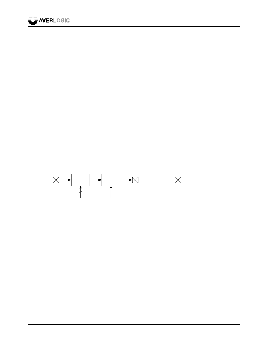
increment is equivalent to approximately 1.6ns. The CKREF delay adjustment diagram is as
follows:
The PLL-generated pixel clock is input from the CKEXT pin, then distributed to different internal or
output pins with different delay for different purposes. The internal logic clock is available at CKAO
pin. The delay-adjustable clock is available at CKBO, which programmability is useful for the
setup/hold time optimization for the LCD controller or any chip that captures the output of the
AL875. The ADC sampling clock is also available at CKADCO pin. The HSFB divider can be up to
4096. The clock distribution circuitry is illustrated in the following diagram:
INV
DELAY
CKREF
4
PHASE A
#0Ch<7:4>
CKREFO-INV
#02h<4>
CKREFO
AL875-07a Clock Reference Delay
Input/Output pin
1 delay = 1.6ns
Max. 15 delays = 24ns

AL875
Preliminary version subject to change without notice February 20, 2003
16
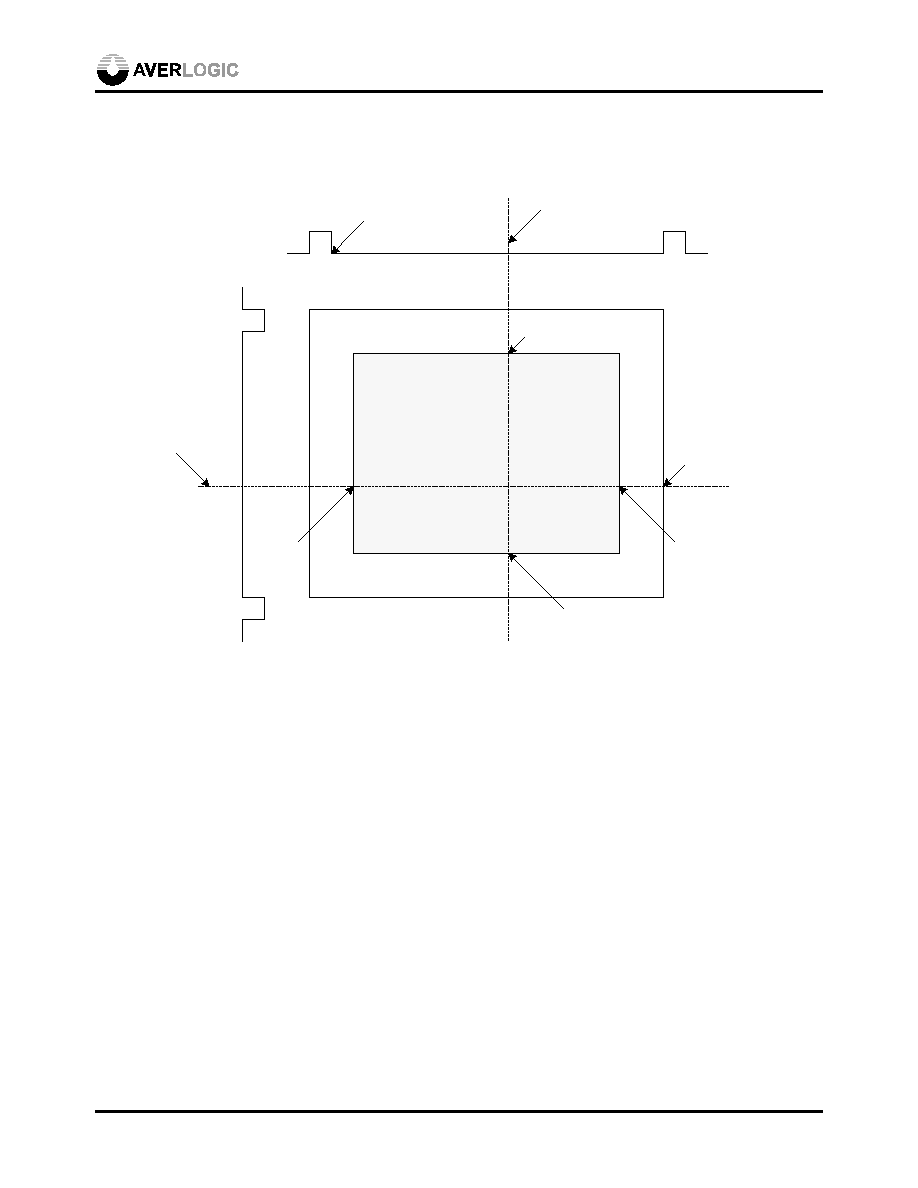
6.4 Automatic Positioning Control
The input horizontal and vertical starting and ending positions are detected to ensure that the whole
picture fits into the displayable region of the screen. Two modes of position detection are provided: 1-
line detection and whole-frame detection. The 1-line detection can be performed by choosing any
horizontal line (reg.#10h) or vertical line (reg.#19h), to check in what range the luma data is larger
than the threshold value defined by DATA_TH (reg.#11h). When the threshold for the vertical line
is different from the horizontal line, an additional register VDATA_TH (reg.#0Fh) can be used for
vertical threshold and it is enabled by reg.#06h<7>. Any luma data lower than the threshold value is
considered blanking period. The following drawing shows the related registers:
DELAY
CKREF
CLOCK
BUFFER
CKAO
PHASE B (#0Ch<3:0>)
CKBO
4
/N
COUNTER
HSFB
DIVIDER
#0Ah<3:0> & #0Bh<7:0>
12
Input/Output pin
AL875-07b Clock Distribution Circuitry
Inverter
INV
CKADCO
ADC sampling clock
Internal logic clock
AL875
Preliminary version subject to change without notice February 20, 2003
17
The whole frame detection scans the whole input video/graphics to check in which range the luma
data is larger than the threshold value defined by DATA_TH or VDATA_TH. Any luma data lower
than the threshold value is considered blanking period. Whole frame detection may be more accurate
than 1-line detection. The following drawing shows the related registers:
INPUT
ACTIVE
REGION
HSYNC
VSYNC
Selected line for vertical positioning detection
VCOLUMN, #19h
Selected line for horizontal
positioning detection
HNUMBER, #10h
VDE_ST,
#1Ah<2:0> & 1Bh<7:0>
HCNT_TOT,
#16h<2:0> & #17h<7:0>
HDE_END,
#14h<2:0> & #15h<7:0>
VDE_END,
#1Ch<2:0> & #1Dh<7:0>
HDE_ST,
#12h<2:0>
& #13h<7:0>
HS_WIDTH, #18h<7:0>
Threshold = DATA_TH, #11h
When horizontal and vertical thresholds are different:
Threshold horizontal = DATA_TH, #11h
Threshold vertical = VDATA_TH, #0Fh, Enabled by #06h<7>
AL875-09 One-line position detection

AL875
Preliminary version subject to change without notice February 20, 2003
18
Details about these registers can be found in the Register Definition section.
6.5 Clock Phase Test (for Jitter-reduction)
The AL875 provides a proprietary clock phase test mode for jitter-reduction. Jitters may be
experienced when sampling clock frequency and/or phase is not accurate. The AL875 can sample
twice (with slightly different clock phases) on each odd or even pixel and count the total output value
difference of the two phases (delay controlled by register #07h). This information (stored in registers
#08h and #09h) is then available for the micro-controller to adjust the sampling clock frequency and
phase for optimization. Additional reference can be found in the Register Definition section.
INPUT
ACTIVE
REGION
HSYNC
VSYNC
WVDE_ST,
#25h<2:0> & #26h<7:0>
WHDE_END,
#23h<2:0> & #24h<7:0>
WVDE_END,
#27h<2:0> & #28h<7:0>
WHDE_ST,
#21h<2:0>
& #22h<7:0>
Threshold = DATA_TH, #11h
When horizontal and vertical thresholds are different:
Threshold horizontal = DATA_TH, #11h
Threshold vertical = VDATA_TH, #0Fh, Enabled by #06h<7>
AL875-10 Whole-frame position detection

AL875
Preliminary version subject to change without notice February 20, 2003
19
6.6 I
2
C Programming
The AL875 I
2
C bus controls and monitors the status of the 3 ADCs, PLL and related registers. Two
pins (ADD1 and ADD2) are used to set the I
2
C address. Therefore, up to four AL875s can be used in
the same system and can be programmed by the same I
2
C bus. For detailed description of the AL875
registers, please refer to the Register Definition Section.
The AL875 I
2
C programming interface follows the Philips standard and consists of the SCL (clock)
and SDA (data) signals. Data can be written to or read from the AL875. For both read and write, each
byte is transferred MSB first, and the SDA data bit is valid when the SCL is pulled high.
The read/write command format is as follows:
Write: <S> <Write SA> <A> <Register Index> <A> <Data> <A> <P>
Read: <S> <Write SA> <A> <Register Index> <A> <S> <Read SA> <A> <Data> <NA> <P>
Following are the details:
<S>:
Start signal
SCL SDA
High High
High Low
The Start signal is HIGH to LOW transition on the
SDA line when SCL is HIGH.
<WRITE SA>:
Write Slave Address: 98h, 9Ah, 9Ch, or 9Eh
<READ SA>:
Read Slave Address: 99h, 9Bh, 9Dh, or 9Fh
<REGISTER INDEX>:
Value of the AL875 register index.
<A>:
Acknowledge stage
The acknowledge-related clock pulse is generated
by the host (master). The host releases the SDA
line (HIGH) for the AL875 (slave) to pull down the
SDA line during the acknowledge clock pulse.
<NA>:
Not Acknowledge stage
SCL
SDA
SDA
SCL
SDA
SCL
SCL
SDA
SCL
Data bit [1] or NA
Data bit [0] or A
START bit [S]
STOP bit [P]
Not significant
AL250-15 I2C drawing

AL875
Preliminary version subject to change without notice February 20, 2003
20
The acknowledge-related clock pulse is generated by the host (master). The host releases the SDA
line (HIGH) during the acknowledge clock pulse, but the AL875 does not pull it down during this
stage.
<DATA>:
Data byte write to or read from the register index.
In read operation, the host must release the SDA line (high) before the first clock pulse is
transmitted to the AL875.
<P>:
Stop signal
SCL SDA
High Low
High High
The Stop signal is LOW to HIGH transition on the SDA line when SCL is HIGH.
Suppose data F0h is to be written to register 0Fh using write slave address 98h, the timing is as
follows:
Suppose data is to be read from register 55h using read slave address 99h, the timing is as follows:
Start
Slave addr = 98h Ack
Ack
Ack Stop
Index = 0Fh
Data = F0h
SDA
SCL
AL875-04 I2C Write timing
Start
Slave addr = 98h
Ack
Ack
Ack
Index = 55h
Read slave addr = 99h
SDA
SCL
AL875-05 I2C Read timing
NAck
Stop
Data read cycle
Stop
Start

AL875
Preliminary version subject to change without notice February 20, 2003
21
More information on the AL875 functionality can be found in the Register Definition section.

AL875
Preliminary version subject to change without notice February 20, 2003
22
7.0 Electrical Characteristics
7.1 Recommended Operating Conditions
Parameter
Min
Max
Unit
VDD
Supply Voltage
+3.0
+3.6
V
TAMB
Ambient Operating Temperature
0
+70
�C
7.2 DC Characteristics
Parameter
Test Conditions
Min
Typ.
Max
Unit
I
DD
Supply current
90MHz
115
mA
P
Power consumption
380
mW
V
IH
Hi-level input voltage
VDD+0.5
-
VDD+0.5
V
V
IL
Lo-level input voltage
+0.8
-
+0.8
V
V
OH
Hi-level output voltage
VDD
-
VDD
V
V
OL
Lo-level output voltage
0.5
-
0.5
V
I
O
Output current, stand data -0.5V<V
O
<V
DD
+0.5
-4
4
mA
Output current, bus driver -0.5V<V
O
<V
DD
+0.5
-12
12
mA
I
LI
Input leakage current
1
-
1
�
A
INL
Integral non-linearity
-
+0.5
+1.3
LSB
DNL Differential non-linearity
-
0.3
0.5
LSB
7.3 AC Characteristics
Parameter
Test Conditions
Min
Typ.
Max
Unit
C
i
Input pin capacitance
-
-
8
PF
CK2
Duty factor (t
CK2H
/t
CK2
)
40
-
60
%
t
iS
Input data set-up time
5
-
-
ns
t
iH
Input data hold time
3
-
-
ns
t
r
Input rise time
Vi = 0.6 to 2.6V
-
-
5
ns
t
f
Input fall time
Vi = 2.6 to 0.6V
-
-
5
ns

AL875
Preliminary version subject to change without notice February 20, 2003
23
C
L
Digital output load cap.
15
-
50
PF
t
oH
Output hold time
C
L
= 15pF
3
-
-
ns
t
PD
Propagation delay
C
L
= 40pF
-
-
5
ns
SNR Signal-to-noise ratio
-
-
48
dB
F
C
Conversion speed
-
-
110
MHz

AL875
Preliminary version subject to change without notice February 20, 2003
24
8.0 AL875 Register Definition
The AL875 is powered up to a default state depending on the hardware mode-setting pins. Hardware
configuration is disabled by setting SoftConfig (bit 4 of register 0x03) as 1, then software
configuration is determined by the values of register 0x02, which is programmable by software.
I2C Sub-address:
ADDR2, ADDR1 pins
I
2
C write address
I
2
C read address
LOW, LOW
98h
99h
LOW, HIGH
9Ah
9Bh
HIGH, LOW
9Ch
9Dh
HIGH, HIGH
9Eh
9Fh
8.1 Index of Control Registers
The following is the summary of AL875 control registers
Register
Addr
R/W
Description
Default
Note
COMPANYID
00h R only Company ID
0100 0110 46h
REVISION
01h R only Revision number
0000 0000 00h
HWCONFIG
02h
R/W Hardware configuration
GENERAL
03h
R/W General register
FAMILY
04h R only Chip family
1000 0111 87h
STATUS
05h
R
Status register
Jitter Test Registers
PHITEST
06h
R/W Clock phase test
UUU0 0000 00h
DELTA
07h
R/W Main and delay clock select
0000 0000
DIFFH
08h R only Difference count in a horizontal line (high)
DIFFL
09h R only Difference count in a horizontal line (low)
PLL-Related Registers
DIVIDERH
0Ah
R/W PLL divider high-byte
0101 0011 53h
DIVIDERL
0Bh
R/W PLL divider low-byte
0100 1000 46h
PHASE
0Ch
R/W PLL phase delay control
0000 0000
One-line Auto-Positioning Registers
HNUMBER
10h
R/W Horizontal line number for HDE_ST,
0000 0110 Unit: 8 lines

AL875
Preliminary version subject to change without notice February 20, 2003
25
HDE_END detection
6 * 8 = 48
DATA_TH
11h
R/W Data threshold for
0001 0000 20h
HDE_STH
12h R only Horizontal active data start (high-byte)
HDE_STL
13h R only Horizontal active data start (low-byte)
HDE_ENDH
14h R only Horizontal active data end (high-byte)
HDE_ENDL
15h R only Horizontal active data end (low-byte)
HCNT_TOTH
16h R only Detected horizontal total value (high-byte)
HCNT_TOTL
17h R only Detected horizontal total value (low-byte)
HS_WIDTH
18h R only Detected horizontal sync width
VCOLUMN
19h
R/W Vertical column number for VDE_ST,
VDE_END detection
0011 0111 Unit: 8 lines
37h * 8=440
VDE_STH
1Ah R only Vertical active data start (high-byte)
VDE_STL
1Bh R only Vertical active data start (low-byte)
VDE_ENDH
1Ch R only Vertical active data end (high-byte)
VDE_ENDL
1Dh R only Vertical active data end (low-byte)
Whole-frame Auto Positioning Registers
WHDE_STH
21h R only Detected horizontal active start pixel
position (high-byte)
WHDE_STL
22h R only Detected horizontal active start pixel
position (low-byte)
WHDE_ENDH
23h R only Detected horizontal active end pixel position
(high-byte)
WHDE_ENDL 23h R only Detected horizontal active end pixel position
(low-byte)
WVDE_STH
25h R only Detected vertical active start line (high byte)
WVDE_STL
26h R only Detected vertical active start line (low-byte)
WVDE_ENDH 27h R only Detected vertical active end line (high-byte)
WVDE_ENDL 28h R only Detected vertical active end line (low-byte)
Note: U � unused
8.2 Register Description
00h: Company ID (R) [COMPANYID]
CompanyId <7:0> Company ID (46h)

AL875
Preliminary version subject to change without notice February 20, 2003
26
01h: Revision (R) [REVISION]
Revision <7:0> Revision number (00h)
02h: Hardware/Software Configuration (R/W) [HWCONFIG]
Ckrefo_inv <4> Invert the phase of CKREFO (reference clock output)
Inv <1> Invert the phase of CKADCO (ADC sampling clock)
PwrDn <0> Power-Down mode (active high)
Please refer to the Clock Distribution Circuitry diagram in section 6.3 for additional reference.
03h: General (R/W) [GENERAL]
If SoftCinfig (0x03<4>) = 0, the values of hardware configuration pins are set/read.
If SoftCinfig (0x03<4>) = 1, the values of software configuration registers are set/read.
SoftConfig <4> Enable configuration defined by software configuration registers
0x02.
04h: Chip Family (R) [FAMILY]
Family <7:0> 10000111, AL875 series
05h: Status Register (R) [STATUS]
VsPol_Det <7> Detected input Vsync polarity 1: positive, 0: negative.
HsPol_Det <6> Detected input Hsync polarity 1: positive, 0: negative.
Vsync <4> Input Vsync signal (without any processing)
Hsync <3> Input Hsync signal (without any processing)
Hspeed <2> Chips speed version; 1: high speed; 0: low speed.
Clock Phase Test (Jitter Test)
06h: Clock Phase Test (R/W) [PHITEST]
ENV_TH <7> Enable VDATA_TH
When ENV_TH = 0, DATA_TH (reg.#11h) applies for both
horizontal and vertical threshold.
When ENV_TH = 1, DATA_TH (reg.#11h) defines horizontal
threshold only; vertical threshold is defined by VDATA_TH
(reg.#0Fh).
ADCDIFF_TH <6:5> Bits 5 and 4 of ADCDIFF_TH, threshold of data difference in clock
phase test mode for auto phase detection
PhiTest <4> Clock phase test enable

AL875
Preliminary version subject to change without notice February 20, 2003
27
ADCDIFF_TH <3:0> Bits 0~3 of ADCDIFF_TH, threshold of data difference in clock
phase test mode for auto phase detection. Any difference lower than
the threshold is considered as noise and can be disregarded.
07h: Delayed Clock value select (R/W) [DELTA]
Delta <3:0> Delayed clock phase-delay select
This register defines the delay of the two ADC sampling clocks in jitter detection mode 1. Each
delay is equivalent to 1.6ns. The detected value is stored in registers #08h and 09h.
08h: Number of pixels with significant data difference in jitter detection mode (R) [DIFFH]
DIFF (9:8) <1:0>
09h: Number of pixels with significant data difference in jitter detection mode (R) [DIFFL]
DIFF (7:0) <7:0>
In this jitter detection mode, all odd pixels in a designated line are sampled and digitized twice.
The total number of data pairs with data value difference higher than the specified threshold value
is stored in these two registers. The delay of the two sampling clocks can be programmed by
register #07h.
Change of HSYNC and clock phase may result in different DIFF values. The lowest DIFF value
usually indicates the optimized HSYNC and clock phase setting.
0Dh: Difference of first and last pixel position (R) [DIFF2H]
DIFF2 (10:8) <2:0> Bits 11~8 of the difference of first and last pixel position
0Eh: Difference of first and last pixel position (R) [DIFF2L]
DIFF2 (7:0) <7:0> Bits 7~0 of the difference of first and last pixel position
In this jitter detection mode, position of the first active pixel of each line is compared with that of
the previous line. When there is difference, this value is incremented by 1. Similarly, position of
the last active pixel of each line is also compared with that of the previous line; when there is
difference, this register values is incremented by 1. The total number is stored in DIFF2Hand
DIFF2L.
PLL-Related Registers
0Ah: Divider High-byte (R/W) [DIVIDERH]
DIVIDERH(11:8) <3:0> Bits 8~11 of the PLL divider
0Bh: Divider Low-byte (R/W) [DIVIDERL]
DIVIDERL(7:0) <7:0> Bits 7~0 of the PLL divider

AL875
Preliminary version subject to change without notice February 20, 2003
28
This is the PLL divider number when a non-programmable genlock PLL such as ICS9173 is used.
0Ch: PLL phase delay control (R/W) [PHASE]
PhaseA <7:4> Hsync phase delay adjustment
PhaseB <3:0> CKBO phase delay adjustment
Refer to the Internal PLL Block Diagram and AL875 Clock Distribution Circuitry in section 6.3
for additional reference.
One-line Automatic positioning:
0Fh: Vertical Data Threshold (R/W) [VDATA_TH]
VData_TH <7:0> Luma (brightness) threshold value.
This value is used to determine non-blanking pixel for vertical direction. Any pixel luma value
less than this value is considered as blanking. . Hardware default value is 32 (20h).
Vertical column used to detect vertical active start and end is defined by register #19h.
This register is enabled by register #06h<7>.
10h: Horizontal Line Number for HDE_ST & HDE_END detection (R/W) [HNUMBER]
HNumber <7:0> Horizontal line number for horizontal active start and end detection; refer
to register #11h for additional reference. (unit: 8 lines)
Hardware default value is 06h, which means 6 X 8 = 48 lines
11h: Data Threshold (R/W) [DATA_TH]
Data_TH <7:0> Luma (brightness) threshold value.
This value is used to determine non-blanking pixel for horizontal direction. Any pixel luma value
less than this value is considered as blanking. . Hardware default value is 32 (20h).
Horizontal line used to detect horizontal active start and end is defined by register #10h.
This register is enabled by register #06h<7>.
12h: Horizontal Active Start High (R only) [HDE_STH]
HDE_stH <2:0> Bits <10:8> of detected horizontal active start pixel position.
13h: Horizontal Active Start Low (R only) [HDE_STL]
HDE_stL <7:0> Bits <7:0> of detected horizontal active start pixel position. (Unit: 1 pixel)
14h: Horizontal Active End High (R only) [HDE_ENDH]
HDE_EndH <2:0> Bits <10:8> of detected horizontal active end-pixel position.
15h: Horizontal Active End Low (R only) [HDE_ENDL]
HDE_EndL <7:0> Bits <7:0> of detected horizontal active end-pixel position. (Unit: 1 pixel)
16h: Detected H Total Value (R only) [HCNT_TOTH]
HCNT_TOTH <2:0> Bits <10:8> of the detected horizontal total pixel number.

AL875
Preliminary version subject to change without notice February 20, 2003
29
17h: Detected H Total Value Low (R only) [HCNT_TOTL]
HCNT_TOTL <7:0> Bits <7:0> of the detected horizontal total pixel number.
18h: Detected Hsync Width (R only) [HS_WIDTH]
HS_WIDTH <7:0> Indicate the detected horizontal sync pulse width.
19h: Vertical Column for VDESTART & VDEEND Detection (R/W) [VCOLUMN]
VColumn <7:0> Vertical column number for vertical active start and end detection; refer to
register #11h for additional reference. Hardware default value: 37h = 55 X
8 = 440. (Unit: 8 pixels)
1Ah: Vertical Active Start High (R only) [VDE_STH]
VDE_StH <2:0> Bits <10:8> of detected vertical active start line.
1Bh: Vertical Active Start Low (R only) [VDE_STL]
VDE_StL <7:0> Bits <7:0> of detected vertical active start line. (Unit: 1 line)
1Ch: Vertical Active End High (R only) [VDEENDH]
VDE_EndH <2:0> Bits <10:8> of detected vertical active end line.
1Dh: Vertical Active End Low (R only) [VDE_ENDL]
VDE_EndL <7:0> Bits <7:0> of detected vertical active end line. (Unit: 1 line)
Whole-frame Automatic positioning:
21h: Horizontal Active Start High (R only) [WHDE_STH]
WHDE_STH <2:0> Bits <10:8> of detected horizontal active start pixel position.
22h: Horizontal Active Start Low (R only) [WHDE_STL]
WHDE_STL <7:0> Bits <7:0> of detected horizontal active start pixel position. (Unit: 1 pixel)
23h: Horizontal Active End High (R only) [WHDE_ENDH]
WHDE_ENDH<2:0> Bits <10:8> of detected horizontal active end pixel position.
24h: Horizontal Active End Low (R only) [WHDE_ENDL]
WHDE_ENDL <7:0> Bits <7:0> of detected horizontal active end pixel position (Unit: 1 pixel)
25h: Vertical Active Start High (R only) [WVDE_STH]
WVDE_STH <2:0> Bits <10:8> of detected vertical active start line
26h: Vertical Active Start Low (R only) [WVDE_STL]
WVDE_STL <7:0> Bits <7:0> of detected vertical active start line (Unit: 1 line)
27h: Vertical Active End High (R only) [WVDE_ENDH]

AL875
Preliminary version subject to change without notice February 20, 2003
30
WVDE_ENDH<2:0> Bits <10:8> of detected vertical active end line
28h: Vertical Active End Low (R only) [WVDE_ENDL]
WVDE_ENDL <7:0> Bits <7:0> of detected vertical active end line (Unit: 1 line)

AL875
Preliminary version subject to change without notice February 20, 2003
31
9.0 Board Design and Layout Considerations
The AL875 contains both precision analog and high-speed digital circuitry. Noise coupling from
digital circuits to analog circuits may result in poor video quality. The layout should be optimized for
lowest noise on the power and ground planes by shielding the digital circuitry and providing good
decoupling.
9.1 Grounding
Analog and digital circuits are separated within the AL875 chip. To minimize system noise and
prevent digital system noise from entering the analog portion, a common ground plane for all devices,
including the AL875 is recommended. All the connections to the ground plane should have very short
leads. The ground plane should be solid, not cross-hatched.
9.2 Power Planes and Power Supply Decoupling
The analog portion of the AL875 and any associated analog circuitry should have their own power
plane, referred to as the analog power plane (AVDD). The analog power plane should be connected to
the digital power plane (DVDD) at a single point through a low resistance ferrite bead. Additionally,
in order to minimize cross interference, the analog power planes of R, G, B and PLL should also be
separated with low resistance ferrite beads.
Power supply connection pins should be individually decoupled. For best results, use 0.1
�
F ceramic
chip capacitors. Lead lengths should be minimized. The power pins should be connected to the
bypass capacitors before being connected to the power planes. 22
�
F capacitors should also be used
between the AL875 power planes and the ground planes to control low-frequency power ripple.
9.3 Digital Signal and Clock Interconnect
Digital signals to the AL875 should be isolated as much as possible from the analog outputs and other
analog circuitry. The high frequency clock reference or crystal should be handled carefully because
jitters and noise on the clock will degrade the video performance. Keep the clock paths to the
decoder as short as possible to reduce noise pickup.
9.4 Analog Signal Interconnect
The AL875 should be located closely to the output connectors to minimize noise and reflections.
Keep the critical analog traces as short and wide as possible (20~30 mil). Digital signals, especially
pixel clocks and data signals should not overlap any of the analog signal circuitry and should be kept
as far apart as possible. The AL875 and the decoder IC should have no inputs left floating.

AL875
Preliminary version subject to change without notice February 20, 2003
32
10.0 Mechanical Drawing
AL875: 14mm x 20mm 100-pin 0.65-pitch PQFP package

AL875
Preliminary version subject to change without notice February 20, 2003
33
11.0 Power Consumption
The AL875 works at single 3.3V power. The following table shows the current consumption of the
AL875 at different operating frequencies.
Frequency
Current
AL875@3.3V
110MHz
135 mA (typ.)
AL875@3.3V
90MHz
115 mA (typ.)
AL875@3.3V
65MHz
95 mA (typ.)
AL875@3.3V
40MHz
65 mA (typ.)
For more information about the AL875 or other AverLogic products, please contact your local
authorized representatives, visit our website, or contact us directly.

CONTACT INFORMATION
Averlogic Technologies Corp.
4F, No. 514, Sec. 2, Cheng Kung Rd., Nei-Hu Dist., Taipei, Taiwan
Tel: +886 2-27915050
Fax: +886 2-27912132
l:
sales@averlogic.com.tw
URL:
http://www.averlogic.com.tw
Averlogic Technologies, Inc.
90 Great Oaks Blvd. #204, San Jose, CA 95119
USA
Tel: 1 408 361-0400
Fax: 1 408 361-0404
E-mail:
sales@averlogic.com
URL:
http://www.averlogic.com