 | –≠–ª–µ–∫—Ç—Ä–æ–Ω–Ω—ã–π –∫–æ–º–ø–æ–Ω–µ–Ω—Ç: AZ100E142 | –°–∫–∞—á–∞—Ç—å:  PDF PDF  ZIP ZIP |

AZ10E142
AZ100E142
ECL/PECL 9-bit Shift Register
1630 S. STAPLEY DR., SUITE 125
∑
MESA, ARIZONA 85204
∑
USA
∑
(480) 962-5881
∑
FAX (480) 890-2541
www.azmicrotek.com
ARIZONA MICROTEK, INC.
FEATURES
∑
700 MHz Minimum Shift Frequency
∑
9-Bit for Byte-Parity Application
∑
Asynchronous Master Reset
∑
Dual Clocks
∑
Operating Range of 4.2V to 5.46V
∑
75k
Internal Input Pulldown Resistors
∑
Direct Replacement for ON Semiconductor
MC10E142 & MC100E142
DESCRIPTION
The AZ10/100E142 is a 9-bit shift register, designed with byte-parity applications in mind. The E142 performs
serial/parallel in and serial/parallel out, shifting in one direction. The nine inputs D0-D8 accept parallel input data,
while S-IN accepts serial input data. The Qn outputs do not need to be terminated for the shift operation to function.
To minimize noise and power, any Q output not used should be left unterminated.
The SEL (Select) input pin is used to switch between the two modes of operation
≠
SHIFT and LOAD. The shift
direction is from bit 0 to bit 8. Input data is accepted by the registers a set-up time before the positive going edge of
CLK1 or CLK2; shifting is also accomplished on the positive clock edge. A HIGH on the Master Reset pin (MR)
asynchronously resets all the registers to zero.
NOTE: Specifications in ECL/PECL tables are valid when thermal equilibrium is established.
26
27
28
1
2
3
4
SEL
D8
D7
D6
V
CCO
D5
Q8
Q7
Q6
V
CC
Q5
V
CCO
Q4
Q3
Q2
Q1
Q0
V
CCO
D4
D3
D2
MR
CLK1
CLK2
V
EE
S-IN
D0
D1
25
24
23
22
21
20
19
18
17
16
15
14
13
12
11
10
9
8
7
6
5
PACKAGE AVAILABILITY
PACKAGE PART
NO. MARKING
PLCC 28
AZ10E142FN
AZM10E142
PLCC 28 T&R AZ10E142FNR2
AZM10E142
PLCC 28
AZ100E142FN
AZM100E142
PLCC 28 T&R AZ100E142FNR2 AZM100E142
Pinout: 28-lead
PLCC (top view)
AZ10E142
AZ100E142
October 2001 * REV - 2
www.azmicrotek.com
2
Absolute Maximum Ratings are those values beyond which device life may be impaired.
Symbol Characteristic
Rating
Unit
V
CC
PECL Power Supply (V
EE
= 0V)
0 to +8.0
Vdc
V
I
PECL Input Voltage (V
EE
= 0V)
0 to +6.0
Vdc
V
EE
ECL Power Supply (V
CC
= 0V)
-8.0 to 0
Vdc
V
I
ECL Input Voltage (V
CC
= 0V)
-6.0 to 0
Vdc
I
OUT
Output Current
--- Continuous
--- Surge
50
100
mA
T
A
Operating Temperature Range
-40 to +85
∞
C
T
STG
Storage Temperature Range
-65 to +150
∞
C
10K ECL DC Characteristics (V
EE
= -4.94V to -5.46V, V
CC
= V
CCO
= GND)
-40
∞
C
0
∞
C
25
∞
C
85
∞
C
Symbol
Characteristic
Min Typ Max Min Typ Max Min Typ Max Min Typ Max
Unit
V
OH
Output
HIGH
Voltage
1
-1080
-890
-1020 -840
-980 -810
-910 -720 mV
V
OL
Output LOW Voltage
1
-1950 -1650
-1950 -1630
-1950 -1630
-1950 -1595 mV
V
IH
Input
HIGH
Voltage -1230 -890
-1170 -840
-1130 -810
-1060 -720 mV
V
IL
Input
LOW
Voltage -1950 -1500
-1950 -1480
-1950 -1480
-1950 -1445 mV
I
IH
Input
HIGH
Current
150
150
150
150
µ
A
I
IL
Input
LOW
Current 0.5 0.5 0.5 0.5
µ
A
I
EE
Power
Supply
Current 120
145 120
145 120
145 120
145 mA
1.
Each output is terminated through a 50
resistor to V
CC
≠ 2V.
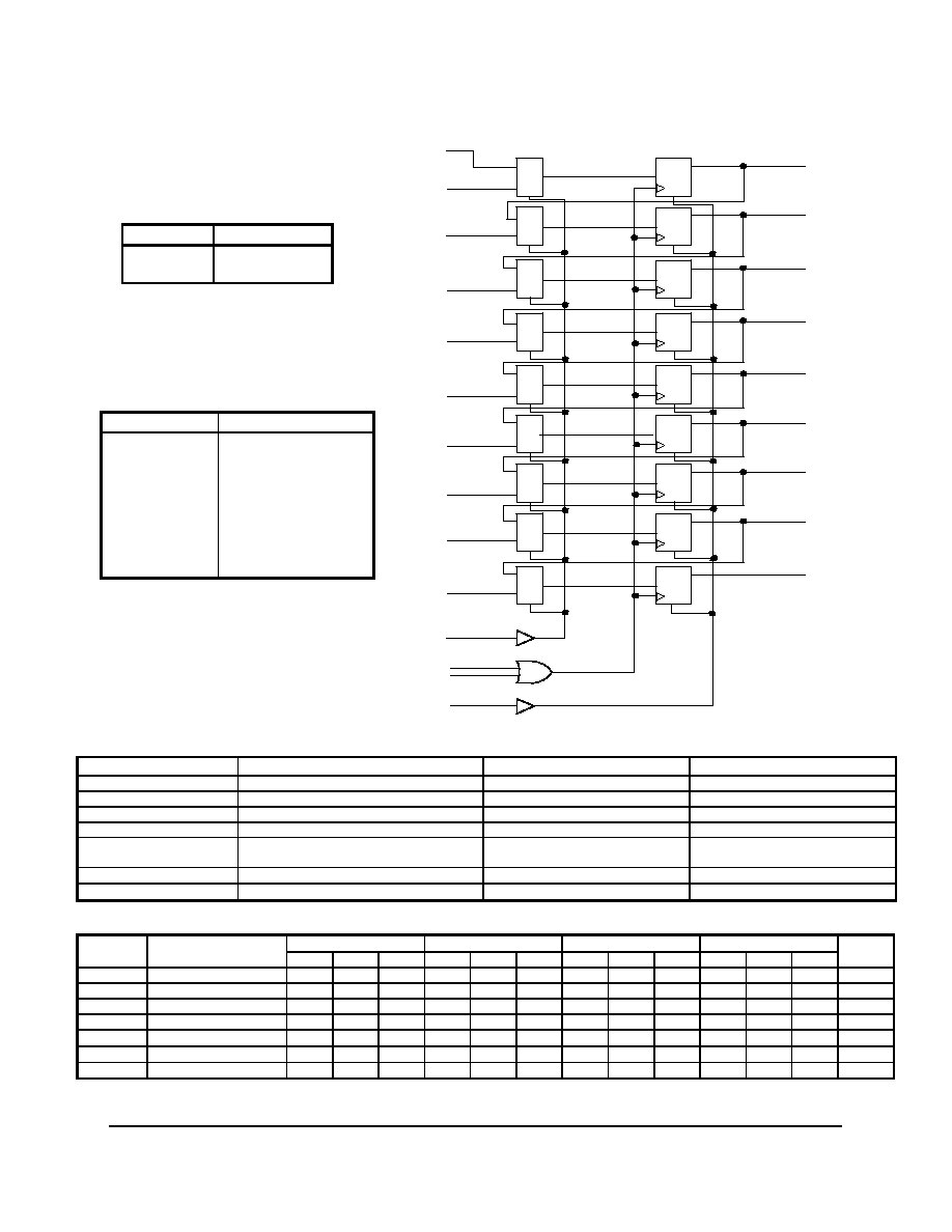
LOGIC SYMBOL
1
0
1
0
1
0
1
0
1
0
1
0
1
0
1
0
1
0
Q
D
Q
D
Q
D
Q
D
Q
D
Q
D
Q
D
Q
D
Q
D
S-IN
D0
D1
D2
D3
D4
D5
D6
D7
D8
SEL
CLK1
CLK2
MR
Q0
Q1
Q2
Q3
Q4
Q5
Q6
Q7
Q8
PIN DESCRIPTION
PIN FUNCTION
D0 ≠ D8
Parallel Data Inputs
S ≠ IN
Serial Data Input
SEL
Mode Select Input
CLK1, CLK2
Clock Inputs
MR Master
Reset
Q0 ≠ Q8
Data Outputs
V
CC
, V
CCO
Positive Supply
V
EE
Negative Supply
FUNCTION TABLE
SEL MODE
L
H
Load
Shift

AZ10E142
AZ100E142
October 2001 * REV - 2
www.azmicrotek.com
3
10K PECL DC Characteristics (V
EE
= GND, V
CC
= V
CCO
= +5.0V)
-40
∞
C 0
∞
C 25
∞
C 85
∞
C
Symbol Characteristic
Min Typ Max
Min
Typ
Max
Min
Typ
Max Min Typ
Max
Unit
V
OH
Output
HIGH
Voltage
1,2
3920 4110
3980 4160
4020 4190
4090 4280 mV
V
OL
Output LOW Voltage
1,2
3050 3350
3050 3370
3050 3370
3050 3405 mV
V
IH
Input
HIGH
Voltage
1
3770 4110
3830 4160
3870 4190
3940 4280 mV
V
IL
Input LOW Voltage
1
3050 3500
3050 3520
3050 3520
3050 3555 mV
I
IH
Input
HIGH
Current
150 150 150 150
µ
A
I
IL
Input
LOW
Current
0.5 0.5 0.5 0.5
µ
A
I
EE
Power
Supply
Current
120
145 120
145 120
145 120
145 mA
1.
For supply voltages other that 5.0V, use the ECL table values and ADD supply voltage value.
2.
Each output is terminated through a 50
resistor to V
CC
≠ 2V.
100K ECL DC Characteristics (V
EE
= -4.2V to -5.46V, V
CC
= V
CCO
= GND)
-40
∞
C
0
∞
C
25
∞
C
85
∞
C
Symbol
Characteristic
Min Typ Max Min Typ Max Min Typ Max Min Typ Max
Unit
V
OH
Output
HIGH
Voltage
1
-1085 -1005 -880 -1025 -955 -880 -1025 -955 -880 -1025 -955 -880 mV
V
OL
Output LOW Voltage
1
-1830 -1695 -1555 -1810 -1705 -1620 -1810 -1705 -1620 -1810 -1705 -1620 mV
V
IH
Input
HIGH
Voltage -1165 -880
-1165 -880
-1165 -880
-1165 -880 mV
V
IL
Input
LOW
Voltage -1810 -1475
-1810 -1475
-1810 -1475
-1810 -1475 mV
I
IH
Input
HIGH
Current
150
150
150
150
µ
A
I
IL
Input
LOW
Current 0.5 0.5 0.5 0.5
µ
A
I
EE
Power
Supply
Current 120
145 120
145 120
145 138
165 mA
1.
Each output is terminated through a 50
resistor to V
CC
≠ 2V.
100K PECL DC Characteristics (V
EE
= GND, V
CC
= V
CCO
= +5.0V)
-40
∞
C 0
∞
C 25
∞
C 85
∞
C
Symbol Characteristic
Min Typ Max
Min
Typ
Max
Min
Typ
Max Min Typ
Max
Unit
V
OH
Output
HIGH
Voltage
1,2
3915 3995 4120 3975 4045 4120 3975 4045 4120 3975 4045 4120 mV
V
OL
Output LOW Voltage
1,2
3170 3305 3445 3190 3295 3380 3190 3295 3380 3190 3295 3380 mV
V
IH
Input
HIGH
Voltage
1
3835 4120
3835 4120
3835 4120
3835 4120 mV
V
IL
Input LOW Voltage
1
3190 3525
3190 3525
3190 3525
3190 3525 mV
I
IH
Input
HIGH
Current
150 150 150 150
µ
A
I
IL
Input
LOW
Current
0.5 0.5 0.5 0.5
µ
A
I
EE
Power
Supply
Current
120
145 120
145 120
145 138
165 mA
1.
For supply voltages other that 5.0V, use the ECL table values and ADD supply voltage value.
2.
Each output is terminated through a 50
resistor to V
CC
≠ 2V.
AC Characteristics (V
EE
= 10E(-4.94V to -5.46V), 100E(-4.2V to -5.46V); V
CC
= V
CCO
= GND or V
EE
= GND,
V
CC
= V
CCO
= 10E(+4.94V to +5.46V), 100E(+4.2V to +5.46V))
-40
∞
C 0
∞
C
25
∞
C
85
∞
C
Unit
Symbol
Characteristic
Min Typ Max Min Typ Max Min Typ Max Min Typ Max
f
SHIFT
Max. Shift Frequency
700
900
700
900 700
900 700
900 MHz
t
PLH
/
t
PHL
Propagation Delay to
Output CLK1, CLK2
MR
600
600
800
800
1000
1000
600
600
800
800
1000
1000
600
600
800
800
1000
1000
600
600
800
800
1000
1000
ps
t
S
Setup Time D
SEL
50
300
-100
150
50
300
-100
150
50
300
-100
150
50
300
-100
150
ps
t
H
Hold Time D
SEL
300
75
100
-150
300
75
100
-150
300
75
100
-150
300
75
100
-150
ps
t
RR
Reset
Recovery
Time
900 700 900 700 900 700 900 700
ps
t
PW
Minimum Pulse Width
CLK1,CLK2, MR
400
400
400
400
ps
t
SKEW
Within-Device
Skew
1
75 75 75 75 ps
t
r
/ t
f
Rise/Fall Times
20% - 80%
300 800
300 800
300 800
300 800 ps
1. Within-device skew is defined as identical transitions on similar paths through a device.

AZ10E142
AZ100E142
October 2001 * REV - 2
www.azmicrotek.com
4
PACKAGE DIAGRAM
PLCC 28
MILLIMETERS INCHES
DIM
MIN MAX MIN MAX
A
12.32 12.57 0.485 0.495
B
12.32 12.57 0.485 0.495
C
4.20 4.57 0.165 0.180
E
2.29 2.79 0.090 0.110
F
0.33 0.48 0.013 0.019
G
1.27 BSC
0.050 BSC
H
0.66 0.81 0.026 0.032
J
0.51 0.020
K
0.64 0.025
R
11.43 11.58 0.450 0.456
U
11.43 11.58 0.450 0.456
V
1.07 1.21 0.042 0.048
W
1.07 1.21 0.042 0.048
X
1.07 1.42 0.042 0.056
T
0.50 0.020
Z
2
O
10
O
2
O
10
O
G1
10.42 10.92 0.410 0.430
K1
1.02 0.040
NOTES:
1.
DATUMS ≠L-, -M-, AND ≠N- DETERMINED
WHERE TOP OF LEAD SHOULDER EXITS
PLASTIC BODY AT MOLD PARTING LINE.
2.
DIMENSION G1, TRUE POSITION TO BE
MEASURED AT DATUM ≠T-, SEATING PLANE.
3.
DIMENSIONS R AND U DO NOT INCLUDE
MOLD FLASH. ALOWABLE MOLD FLASH IS
0.010mm (0.250in.) PER SIDE.
4.
DIMENSIONING AND TOLERANCING PER ANSI
Y14.5M, 1982.
5.
CONTROLLING DIMENSION: INCH.
6.
THE PACKAGE TOP MAY BE SMALLER THAN
THE PACKGE BOTTOM BY UP TO 0.012mm
(0.300in.). DIMENSIONS R AND U ARE
DETERMINED AT THE OUTERMOST
EXTREMES OF THE PLASTIC BODY
EXCLUSIVE OF MOLD FLASH, THE BAR
BURRS, GATE BURRS AND INTERLEAD FLASH,
BUT INCLUDING ANY MISMATCH BETWEEN
THE TOP AND BOTTOM OF THE PLASTIC
BODY.
7.
DIMENSION H DOES NOT INCLUDE DAMBAR
PROTRUSION OR INTRUSION. THE DAMBAR
PROTRUSION(S) SHALL NOT CAUSE THE H
DIMENSION TO BE SMALLER THAN 0.025mm
(0.635in.).

AZ10E142
AZ100E142
October 2001 * REV - 2
www.azmicrotek.com
5
Arizona Microtek, Inc. reserves the right to change circuitry and specifications at any time without prior notice. Arizona Microtek, Inc.
makes no warranty, representation or guarantee regarding the suitability of its products for any particular purpose, nor does Arizona
Microtek, Inc. assume any liability arising out of the application or use of any product or circuit and specifically disclaims any and all
liability, including without limitation special, consequential or incidental damages. Arizona Microtek, Inc. does not convey any license
rights nor the rights of others. Arizona Microtek, Inc. products are not designed, intended or authorized for use as components in systems
intended to support or sustain life, or for any other application in which the failure of the Arizona Microtek, Inc. product could create a
situation where personal injury or death may occur. Should Buyer purchase or use Arizona Microtek, Inc. products for any such
unintended or unauthorized application, Buyer shall indemnify and hold Arizona Microtek, Inc. and its officers, employees, subsidiaries,
affiliates, and distributors harmless against all claims, costs, damages, and expenses, and reasonable attorney fees arising out of, directly
or indirectly, any claim of personal injury or death associated with such unintended or unauthorized use, even if such claim alleges that
Arizona Microtek, Inc. was negligent regarding the design or manufacture of the part.