
AZ10LVEL16VS
AZ100LVEL16VS
ECL/PECL Differential Receiver with Variable Output Swing
1630 S. STAPLEY DR., SUITE 125
∑
MESA, ARIZONA 85204
∑
USA
∑
(480) 962-5881
∑
FAX (480) 890-2541
www.azmicrotek.com
ARIZONA MICROTEK, INC.
FEATURES
∑
250ps Propagation Delay
∑
High Bandwidth Output Transitions
∑
Operating Range of 3.0V to 5.5V
∑
Internal Input Pulldown Resistors
∑
Functionally Equivalent to ON
Semiconductor MC10EL16, MC100EL16
& MC100LVEL16
∑
Variable Output Swing
DESCRIPTION
The AZ10/100LVEL16VS is a differential receiver with variable output swing. The LVEL16VS has
functionality and output transition times similar to the EL16, with an input that controls the amplitude of the Q/Q
Ø
outputs.
The operational range of the LVEL16VS control input, V
CTRL
, is from V
BB
(full swing) to V
CC
(min. swing).
Maximum swing is achieved by leaving the V
CTRL
pin open or by tying it to the negative supply (V
EE
). Simple
control of the output swing can be obtained by a variable resistor between the V
BB
and V
CC
pins, with the wiper
driving V
CTRL
. Typical application circuits and results are described in this Data Sheet.
The LVEL16VS provides a V
BB
output for single-ended use or a DC bias reference for AC coupling to the
device. For single-ended input applications, the V
BB
reference should be connected to one side of the D/D
Ø
differential input pair. The input signal is then fed to the other D/D
Ø input. The V
BB
pin can support 1.5mA
sink/source current. When used, the V
BB
pin should be bypassed to ground via a 0.01
µ
F capacitor.
Under open input conditions internal input clamps will force the Q output LOW.
NOTE: Specifications in the ECL/PECL tables are valid when thermal equilibrium is established.
PACKAGE AVAILABILITY
PACKAGE PART
NO.
MARKING
SOIC 8
AZ10LVEL16VSD
AZM10LVEL16VS
SOIC 8 T&R
AZ10LVEL16VSDR1
AZM10LVEL16VS
SOIC 8 T&R
AZ10LVEL16VSDR2
AZM10LVEL16VS
SOIC 8
AZ100LVEL16VSD
AZM100LVEL16VS
SOIC 8 T&R
AZ100LVEL16VSDR1 AZM100LVEL16VS
SOIC 8 T&R
AZ100LVEL16VSDR2 AZM100LVEL16VS
TSSOP 8
AZ10LVEL16VST
AZTL16VS
TSSOP 8 T&R AZ10LVEL16VSTR1
AZTL16VS
TSSOP 8 T&R AZ10LVEL16VSTR2
AZTL16VS
TSSOP 8
AZ100LVEL16VST
AZHL16VS
TSSOP 8 T&R AZ100LVEL16VSTR1 AZHL16VS
TSSOP 8 T&R AZ100LVEL16VSTR2 AZHL16VS

AZ10LVEL16VS
AZ100LVEL16VS
October 2001 * REV - 0
www.azmicrotek.com
2
Absolute Maximum Ratings are those values beyond which device life may be impaired.
Symbol Characteristic
Rating Unit
V
CC
PECL Power Supply (V
EE
= 0V)
0 to +8.0
Vdc
V
I
PECL Input Voltage (V
EE
= 0V)
0 to +6.0
Vdc
V
EE
ECL Power Supply (V
CC
= 0V)
-8.0 to 0
Vdc
V
I
ECL Input Voltage (V
CC
= 0V)
-6.0 to 0
Vdc
I
OUT
Output Current
--- Continuous
--- Surge
50
100
mA
T
A
Operating Temperature Range
-40 to +85
∞
C
T
STG
Storage Temperature Range
-65 to +150
∞
C
10K ECL DC Characteristics (V
EE
= -3.0V to -5.5V, V
CC
= GND)
-40
∞
C
0
∞
C
25
∞
C
85
∞
C
Symbol
Characteristic
Min Typ Max Min Typ Max Min Typ Max Min Typ Max
Unit
V
OH
Output
HIGH
Voltage
2
-1080
-890
-1020 -840
-980 -810
-910 -720 mV
V
OL
Output LOW Voltage
2
V
CTRL
= V
BB
1
-1950 -1650
-1950 -1630
-1950 -1630
-1950 -1595 mV
V
OL
Output LOW Voltage
2
V
CTRL
= V
CC
-1220 -1030
-1200 -1020
-1190
-1150
-1020
-1190 -1000 mV
V
IH
Input
HIGH
Voltage -1230 -890
-1170 -840
-1130 -810
-1060 -720 mV
V
IL
Input
LOW
Voltage -1950 -1500
-1950 -1480
-1950 -1480
-1950 -1445 mV
V
BB
Reference
Voltage
-1450 -1300
-1400 -1270
-1370 -1250
-1330 -1190 mV
I
IH
Input HIGH Current
D, D
Ø
V
CTRL
150
40
150
40
150
40
150
40
µ
A
I
IL
Input LOW Current
D, D
Ø
V
CTRL
-150
0.5
-150
0.5
-150
0.5
-150
0.5
µ
A
I
EE
Power
Supply
Current 18 25 18 25 18 25 21 26 mA
1. If
V
CTRL
is Open Circuit, use the V
OH
(Max & Min) and V
OL
(V
CTRL
= V
BB
: Max only) limits.
2.
Each output is terminated through a 50
resistor to V
CC
≠ 2V.
8
5
6
7
4
3
2
1
VCC
D
VEE
Q
Q
VBB
D
VCTRL
LOGIC DIAGRAM AND PINOUT ASSIGNMENT
PIN DESCRIPTION
PIN FUNCTION
D, D
Ø Data
Inputs
V
CTRL
Output Swing Control
Q, Q
Ø Data
Outputs
V
BB
Reference Voltage Output
V
CC
Positive
Supply
V
EE
Negative Supply

AZ10LVEL16VS
AZ100LVEL16VS
October 2001 * REV - 0
www.azmicrotek.com
3
10K LVPECL DC Characteristics (V
EE
= GND, V
CC
= +3.3V)
-40
∞
C 0
∞
C 25
∞
C 85
∞
C
Symbol Characteristic
Min Typ Max
Min
Typ
Max
Min
Typ
Max Min Typ
Max
Unit
V
OH
Output
HIGH
Voltage
1,3
2220 2410
2280 2460
2320 2490
2390 2580 mV
V
OL
Output LOW Voltage
1,3
V
CTRL
= V
BB
2
1350 1650
1350 1670
1350 1670
1350 1705 mV
V
OL
Output LOW Voltage
1,3
V
CTRL
= V
CC
2080 2270 2100 2280 2110 2150 2280 2110 2300 mV
V
IH
Input
HIGH
Voltage
1
2070 2410
2130 2460
2170 2490
2240 2580 mV
V
IL
Input LOW Voltage
1
1350 1800
1350 1820
1350 1820
1350 1855 mV
V
BB
Reference
Voltage
1
1850 2000
1900 2030
1930 2050
1970 2110 mV
I
IH
Input HIGH Current
D, D
Ø
V
CTRL
150
40
150
40
150
40
150
40
µ
A
I
IL
Input LOW Current
D, D
Ø
V
CTRL
-150
0.5
-150
0.5
-150
0.5
-150
0.5
µ
A
I
EE
Power
Supply
Current 18 25 18 25 18 25 21 26 mA
1.
For supply voltages other that 3.3V, use the ECL table values and ADD supply voltage value.
2. If
V
CTRL
is Open Circuit, use the V
OH
(Max & Min) and V
OL
(V
CTRL
= V
BB
: Max only) limits.
3.
Each output is terminated through a 50
resistor to V
CC
≠ 2V.
10K PECL DC Characteristics (V
EE
= GND, V
CC
= +5.0V)
-40
∞
C 0
∞
C 25
∞
C 85
∞
C
Symbol Characteristic
Min Typ Max
Min
Typ
Max
Min
Typ
Max Min Typ
Max
Unit
V
OH
Output
HIGH
Voltage
1,3
3920 4110
3980 4160
4020 4190
4090 4280 mV
V
OL
Output LOW Voltage
1,3
V
CTRL
= V
BB
2
3050 3350
3050 3350
3050 3350
3050 3405 mV
V
OL
Output LOW Voltage
1,3
V
CTRL
= V
CC
3780 3970 3800 3980 3810 3850 3980 3810 4000 mV
V
IH
Input
HIGH
Voltage
1
3770 4110
3830 4160
3870 4190
3940 4280 mV
V
IL
Input LOW Voltage
1
3050 3500
3050 3520
3050 3520
3050 3555 mV
V
BB
Reference
Voltage
1
3550 3700
3600 3730
3630 3750
3670 3810 V
I
IH
Input HIGH Current
D, D
Ø
V
CTRL
150
40
150
40
150
40
150
40
µ
A
I
IL
Input LOW Current
D, D
Ø
V
CTRL
-150
0.5
-150
0.5
-150
0.5
-150
0.5
µ
A
I
EE
Power
Supply
Current 18 25 18 25 18 25 21 26 mA
1.
For supply voltages other that 5.0V, use the ECL table values and ADD supply voltage value.
2. If
V
CTRL
is Open Circuit, use the V
OH
(Max & Min) and V
OL
(V
CTRL
= V
BB
: Max only) limits.
3.
Each output is terminated through a 50
resistor to V
CC
≠ 2V.
100K ECL DC Characteristics (V
EE
= -3.0V to -5.5V, V
CC
= GND)
-40
∞
C
0
∞
C
25
∞
C
85
∞
C
Symbol
Characteristic
Min Typ Max Min Typ Max Min Typ Max Min Typ Max
Unit
V
OH
Output
HIGH
Voltage
2
-1085 -1005 -880 -1025 -955 -880 -1025 -955 -880 -1025 -955 -880 mV
V
OL
Output LOW Voltage
2
V
CTRL
= V
BB
1
-1890 -1620
-1870 -1680
-1870
-1775
-1680
-1870 -1680 mV
V
OL
Output LOW Voltage
2
V
CTRL
= V
CC
-1180
-975 -1135
-990 -1135 -1065 -990 -1135
-990 mV
V
IH
Input
HIGH
Voltage -1165 -880
-1165 -880
-1165 -880
-1165 -880 mV
V
IL
Input
LOW
Voltage -1810 -1475
-1810 -1475
-1810 -1475
-1810 -1475 mV
V
BB
Reference
Voltage
-1420 -1260
-1420 -1260
-1420 -1260
-1420 -1260 mV
I
IH
Input HIGH Current
D, D
Ø
V
CTRL
150
40
150
40
150
40
150
40
µ
A
I
IL
Input LOW Current
D, D
Ø
V
CTRL
-150
0.5
-150
0.5
-150
0.5
-150
0.5
µ
A
I
EE
Power
Supply
Current 18 25 18 25 18 25 21 26 mA
1. If
V
CTRL
is Open Circuit, use the V
OH
(Max & Min) and V
OL
(V
CTRL
= V
BB
: Max only) limits.
2.
Each output is terminated through a 50
resistor to V
CC
≠ 2V.

AZ10LVEL16VS
AZ100LVEL16VS
October 2001 * REV - 0
www.azmicrotek.com
4
100K LVPECL DC Characteristics (V
EE
= GND, V
CC
= +3.3V)
-40
∞
C 0
∞
C 25
∞
C 85
∞
C
Symbol Characteristic
Min Typ Max
Min
Typ
Max
Min
Typ
Max Min Typ
Max
Unit
V
OH
Output
HIGH
Voltage
1,3
2215 2295 2420 2275 2345 2420 2275 2345 2420 2275 2345 2420 mV
V
OL
Output LOW Voltage
1,3
V
CTRL
= V
BB
2
1410 1680 1430 1620 1430 1525 1620 1430 1620 mV
V
OL
Output LOW Voltage
1,3
V
CTRL
= V
CC
2120 2325 2165 2310 2165 2235 2310 2165 2310
mV
V
IH
Input
HIGH
Voltage
1
2135 2420
2135 2420
2135 2420
2135 2420 mV
V
IL
Input LOW Voltage
1
1490 1825
1490 1825
1490 1825
1490 1825 mV
V
BB
Reference
Voltage
1
1880 2040
1880 2040
1880 2040
1880 2040 mV
I
IH
Input HIGH Current
D, D
Ø
V
CTRL
150
40
150
40
150
40
150
40
µ
A
I
IL
Input LOW Current
D, D
Ø
V
CTRL
-150
0.5
-150
0.5
-150
0.5
-150
0.5
µ
A
I
EE
Power
Supply
Current 18 25 18 25 18 25 21 26 mA
1.
For supply voltages other that 3.3V, use the ECL table values and ADD supply voltage value.
2. If
V
CTRL
is Open Circuit, use the V
OH
(Max & Min) and V
OL
(V
CTRL
= V
BB
: Max only) limits.
3.
Each output is terminated through a 50
resistor to V
CC
≠ 2V.
100K PECL DC Characteristics (V
EE
= GND, V
CC
= +5.0V)
-40
∞
C 0
∞
C 25
∞
C 85
∞
C
Symbol Characteristic
Min Typ Max
Min
Typ
Max
Min
Typ
Max Min Typ
Max
Unit
V
OH
Output
HIGH
Voltage
1,3
3915 3995 4120 3975 4045 4120 3975 4045 4120 3975 4045 4120 mV
V
OL
Output LOW Voltage
1,3
V
CTRL
= V
BB
2
3110 3380 3130 3320 3130 3225 3320 3130 3320 mV
V
OL
Output LOW Voltage
1,3
V
CTRL
= V
CC
3820 4025 3865 4010 3865 3935 4010 3865 4010 mV
V
IH
Input
HIGH
Voltage
1
3820 4025 3865 4010 3865 3935 4010 3865 4010 mV
V
IL
Input LOW Voltage
1
3835 4120
3835 4120
3835 4120
3835 4120 mV
V
BB
Reference
Voltage
1
3580 3740
3580 3740
3580 3740
3580 3740 V
I
IH
Input HIGH Current
D, D
Ø
V
CTRL
150
40
150
40
150
40
150
40
µ
A
I
IL
Input LOW Current
D, D
Ø
V
CTRL
-150
0.5
-150
0.5
-150
0.5
-150
0.5
µ
A
I
EE
Power
Supply
Current 18 25 18 25 18 25 21 26 mA
1.
For supply voltages other that 5.0V, use the ECL table values and ADD supply voltage value.
2. If
V
CTRL
is Open Circuit, use the V
OH
(Max & Min) and V
OL
(V
CTRL
= V
BB
: Max only) limits.
3.
Each output is terminated through a 50
resistor to V
CC
≠ 2V.
AC Characteristics (V
EE
= -3.0V to -5.5V; V
CC
= GND; V
CTRL
=V
BB
or V
EE
=GND; V
CC
= +3.0V to +5.5V; V
CTRL
=V
BB
)
-40
∞
C
0
∞
C
25
∞
C
85
∞
C
Symbol
Characteristic
Min Typ Max Min Typ Max Min Typ Max Min Typ Max
Unit
t
PLH
/ t
PHL
Input to
Output Delay
(DIFF)
(SE)
250
250
175
125
250
250
325
375
175
125
250
250
325
375
205
155
280
280
355
405
ps
ps
t
SKEW
Duty Cycle Skew
1
(Diff)
5 5 20 5 20 5 20
ps
V
PP
(AC) Minimum
Input
Swing
2
150 150 150 150 mV
V
CMR
Common Mode Range
3
V
PP
< 500mV
V
PP
500mV
V
EE
+
1.2
1.5
V
CC
-
0.4
0.4
V
EE
+
1.1
1.4
V
CC
-
0.4
0.4
V
EE
+
1.1
1.4
V
CC
-
0.4
0.4
V
EE
+
1.1
1.4
V
CC
-
0.4
0.4
V
t
r
/ t
f
Output Rise/Fall Times Q
(20% - 80%)
100 260
100 260
100 260
100 260
ps
1. Duty cycle skew is the difference between a t
PLH
and t
PHL
propagation delay through a device.
2. V
PP
is the minimum peak-to-peak differential input swing for which AC parameters are guaranteed.
3. The V
CMR
range is referenced to the most positive side of the differential input signal. Normal operation is obtained if the HIGH level falls within
the specified range and the peak-to-peak voltage lies between V
PP
(min) and 1V.
AZ10LVEL16VS
AZ100LVEL16VS
October 2001 * REV - 0
www.azmicrotek.com
5
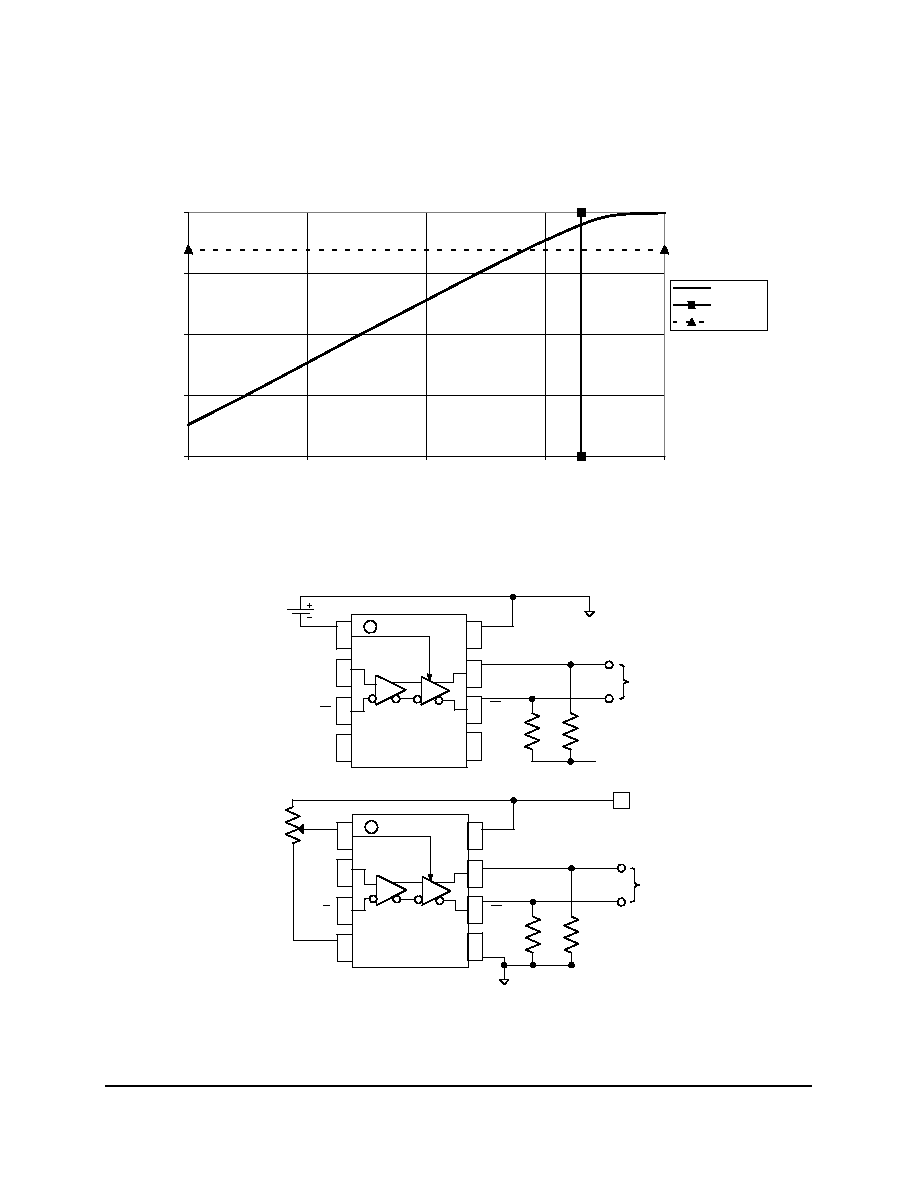
Typical Voltage Output Swing at +25C, V
CC
Nom (see Figure 1 and
Figure 2)
Vbb
1.320
1.500 V (100K ECL)
0
25
50
75
100
0.0
0.4
0.8
1.2
1.6
V
CTRL
(V)
V
SWIN
G
(% pk-pk differential)
%OUT
Vbb
100K ECL
Figure 2: Alternative Implementation
8
5
6
7
4
3
2
1
V CC
D
VEE
Q
Q
VBB
D
V
CTRL
V
CTRL
50
-2V
50
V
SWING
(pk-pk)
Figure 1: Voltage Source Implementation
8
5
6
7
4
3
2
1
V CC
D
VEE
Q
Q
VBB
D
VCTRL
R
L
R
L
10k
V
SWING
(pk-pk)
RL = 180@3.3V Supply; RL = 330@5.0V Supply