 | ÐлекÑÑоннÑй компоненÑ: AGM1216A | СкаÑаÑÑ:  PDF PDF  ZIP ZIP |
Äîêóìåíòàöèÿ è îïèñàíèÿ www.docs.chipfind.ru

Page 1 of 12
SPECIFICATIONS FOR
LIQUID CRYSTAL DISPLAY
PART NUMBER: AGM1216A
DATE:
AZ DISPLAYS, INC.
September 16, 2004
AGM1216A
Page 2 of 12
1. Initial Release 09/16/04
REVISION HISTORY
Date
Version
Content
A
AGM1216A
Page 3 of 12
1.0 LCD Module Characteristics
Units
No.
Item
Characteristics
(1)
Module Size
37.2 (W) x 50.6 (H) x 3.1 (T)
mm
(2)
Format
128 x (R.G.B.) x 160
Dots
(3)
Active Area
32.05 (W) x 38.9 (H)
mm
(4)
Dot Size
0.065 (W) x 0.215 (H)
mm
mm
(5)
Dot Pitch
0.075 (w) x 0.225 (H)
(6)
Approximate Weight
g
TBD
(7)
LCD Type
CSTN (Negative/ Transmissive)
(8)
Drive Method
Duty: 1/160 Bias: 1/11
(9)
Viewing Direction
6 O'clock
(10)
Back Light
White LED
(11)
Drivers
S-44205A (Supports 4096, 65K colors)
AZ DISPLAYS, INC.
1.2
Mechanical Diagram
1.2.1 LCD
Diagram
AZ DISPLAYS, INC.
AGM1216A
Page 4 of 12
1.2.2 LCM
Diagram
AZ DISPLAYS, INC.
AGM1216A
Page 5 of 12
Page 6 of 12
AZ DISPLAYS, INC.
AGM1216A
2.0 Absolute Maximum Rating
Gnd = 0V, Ta = 25 C
Item
Symbol
Min.
Max.
Unit
Power Supply Logic Voltage
V
-0.3
+4.0
V
V
-0.3
+7.0
Power Supply EEPROM
CC
Power Supply Negative Voltage
V
-7.38
V
CL
Contrast Voltage
V
DD
V
DD
V
CL
-
+18.38
V
2.1 Environmental Absolute Maximum
Item
Storage
Operating
Remarks
Ambient Temperature
Min,
Max.
Max.
Min,
-20 C
70 C
-30 C
80 C
Note 1
Humidity
Note 2. Temp at < 40 C, 85% RH MAX.
Note 1. Ta at -20 C -----< 48 hours, at 70 C ----< 120 hours.
No Condensation
Note 2, 3
Note 3. Temp > 40 C, Absolute humidity must be less than 85% RH
Item
Symbol
Min.
Supply Logic Voltage
V
EEPROM Voltage
CC
"H" Input Voltage
V
IH
"L" Input Voltage
V
DD
V
IL
Max.
Unit
V
V
V
V
2.4
Typ.
3.0
3.3
2.7
3.0
5.5
0.8 V
DD
V
DD
0
0.2 V
DD
"H" Output Voltage
V
OH
V
I
DD
"L" Output Voltage
Supply Current
2
0.4
V
V
mA
V
DD
-0.4
-
-
-
-
-
-
-
-
Note 4
Note 5
Note 6
Note 4. I = -1 mA
OH
Note 5. I = 1 mA
OL
Note 6. V = 3.0 V
DD
3.0 Electrical Characteristics
4.0 Optical
Characteristics
AGM1216A
Item
Symbol
Condition
Min.
Typ.
Max.
Unit
Remark
LCD Driving Voltage
V
-20 C
25 C
70 C
(15.2)
(16.2)
(17.2)
V
(14.6)
(15.6)
(16.6)
(13.8)
(14.8)
(15.8)
Response
Time
Rise
Fall
Tr
Tf
0=o=O
0=o=O
-
-
l
l
25 C
25 C
(150)
(230)
(150)
(230)
ms
ms
Contrast ratio
CR
0=o=O
- l
(18.0)
(30.0)
Transmittance
T
(3.6)
(6.0)
Chromaticity
Coordinates
White
Red
Green
X
X
X
X
Y
Y
Y
Y
0=o=O
- l
0=o=O
- l
0=o=O
- l
(0.25)
(0.30)
(0.35)
(0.27)
(0.32)
(0.37)
(0.47)
(0.52)
(0.57)
(0.29)
(0.34)
(0.55)
(0.39)
(0.39)
(0.34)
(0.50)
(0.45)
(0.29)
0=o=O
- l
Blue
(0.12)
(0.17)
(0.22)
(0.12)
(0.17)
(0.22)
Color Gamut (NTSC)
S
(26)
%
Ta = 25 C
Note 1.
Note 2.
Note 1. Duty driven using the LCD7000 (fFRM = 100 Hz, 1/160 duty, 1/11 bias)
Note 2. Duty driven using actual driver IC.
Note 3. All (figures) are estimates only.
o = O = 0
l
+X
-X
+Y
-Y
-
0-
ol
Definition of viewing angle.
CR Max.
Vop
Driving voltage
AZ DISPLAYS, INC.
Definition of Contrast Ratio
Page 7 of 12
5.
0 Interface Pin Function
NO SYMBOL
FUNCTION
1 DISP
TRST = H (Display off)
Making /DISP low sets the D1 flag to 0 and the D0 flag to 0 (D1 =
D0 = 0) in the driver output control register (08h) and turns OFF the
display. To light the display after it has been turned OFF by this pin,
make /DISP high and set the D1 flag to 1 and the D0 flag to 1
(D1 = 1, D0 = 1).
2 VSS
Ground pin, connected to 0 V
3 VCC
This pin is the power supply pin for EEPROM.
connects to +2.7 V to +5.5 V
4 VDD
Power supply pin, connects to +2.4 V to +3.3 V
5 /CS1
The pin is chip select signal pin. When /CS1 = L, the
chip is active, and data/commands can be input or output and I/O manipulated.
6 RS
This pin is usually connected to the least significant bit of a standard CPU
address bus to identify whether data is an index register or data/command.
RS = H: Indicates that D0 to D7 or D0 to D15 are data/command.
RS = L: Indicates that D0 to D7 or D0 to D15 are an index register.
7 /WR
When i80 system parallel data transfer is selected (/WR), write is enabled
by this signal. Data is written at the rising edge of this signal. When M68
system parallel data transfer is selected, this pin determines the
data transfer direction, as follows:
0: Write 1: Read
8 /RD
When i80 system parallel data transfer is selected (/RD), read is enabled
by this signal. When this pin is L, data is output to the data bus. When
M68 system parallel data transfer is selected, this pin inputs an enable
signal that triggers data write or read.
9 PSX
L: Serial
H: Parallel
10 S80X
L: I80 system CPU mode
H: M68 system CPU mode
11 BMOD
L: 16bit data bus
H: 8bit data bus
AZ DISPLAYS, INC.
AGM1216A
Page 8 of 12
NO SYMBOL
FUNCTION
12 DB0
13 DB1
14 DB2
15 DB3
16 DB4
17 DB5
18 DB6(SCL)
19 DB7(SI)
20 DB8
21 DB9
22 DB10
23 DB11
24 DB12
25 DB13
26 DB14
27 DB15
This is a bidirectional data bus connected to an 8-bit or 16-bit standard
CPU bus. When the serial interface is selected (PSX = L), D7 functions as
a serial data input pin (SI), and D6 serves as a serial clock input pin (SCL).
At this time, D0 to D5 and D8 to D15 go into a high-impedance state.
When the 8-bit data bus is selected, only D0 to D7 are used, and D8 to D15
go into a high-impedance state. Data is input starting from its higher byte,
followed by the lower byte. If the chip is not selected, all D0 to D15 go into
high-impedance state.
AZ DISPLAYS, INC.
AGM1216A
Page 9 of 12
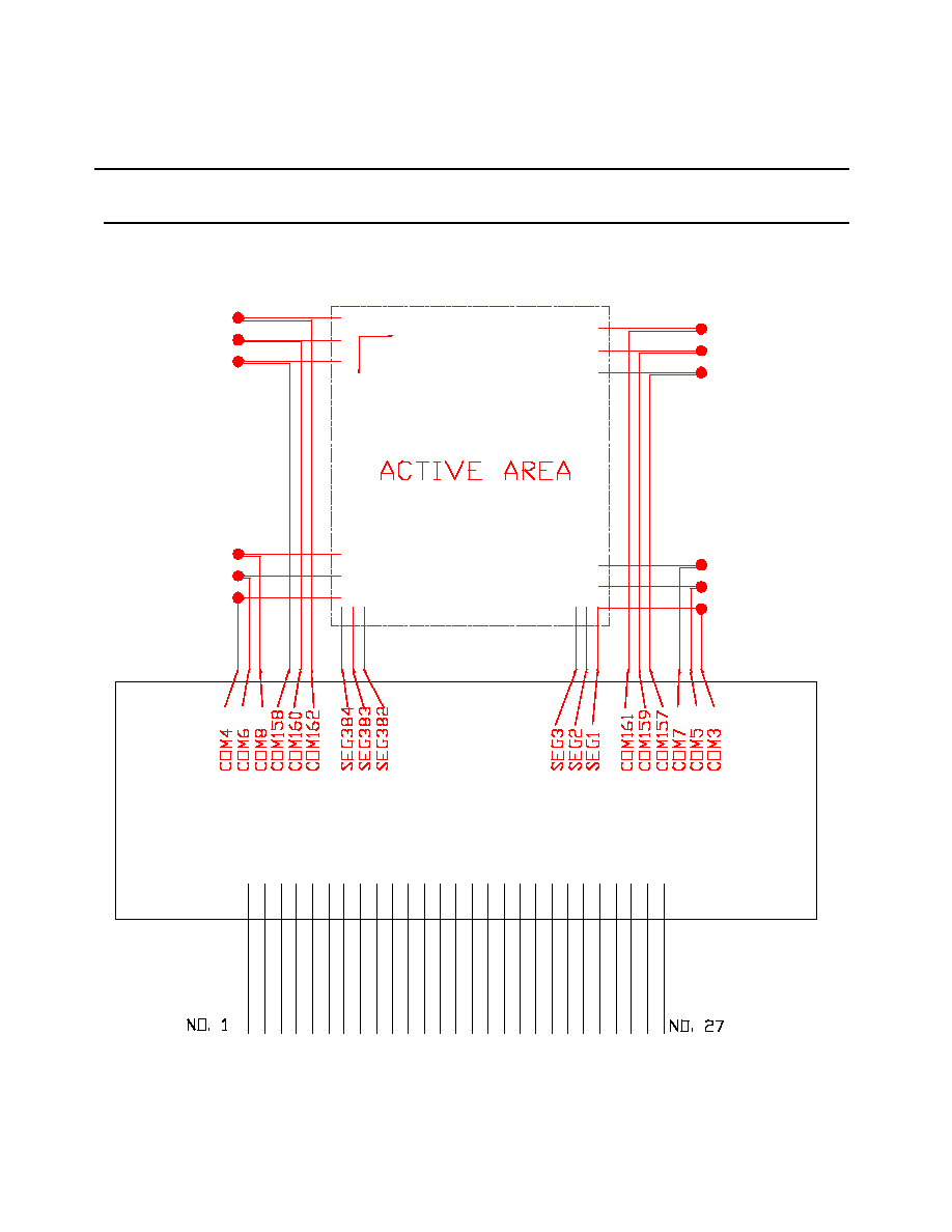
6.
0 Block Diagram
AZ DISPLAYS, INC.
AGM1216A
Page 10 of 12
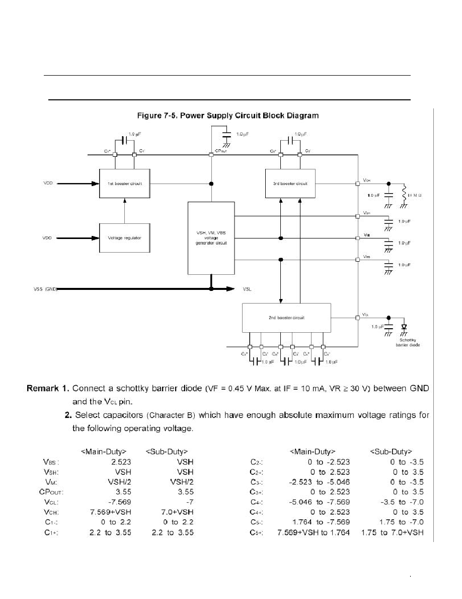
7.
0 Power supply for LCD module
AZ DISPLAYS, INC.
AGM1216A
Page 11 of 12
AZ DISPLAYS, INC.
AGM1216A
Page 12 of 12
8.0 Backlight Characteristics
1. Electrical Ratings:
The LED chips are distibuted over the entire lighted are to provide the most uniform
lighting.
Item
Symbol
Condition
Min.
Typ.
Max.
Unit
Forward Voltage
Reverse Voltage
Luminance
LED color
Vf
Vr
Lv
White
If=15 mA
10
10.2
V
V
cd/m
5.0
-
-
1600
1800
-
If=15 mA
2
2. Internal Circuit Diagram
A
K
>l
l
>l
l
>l
l
> l
l
o
o
For operation above 25 C, the electical ratings must be derated. The value of the current derating is
-0.36 mA / degree C for DC drive and -0.86 mA / degree C for Pulse drive. Power dissipation is 0.75
mW / degree C.
3. Measurement Method
The luminance is the average value of 5 points. The ratio of Lv min. / Lv
max. is greater than 0.8 cd/m. The minimum ratio is 0.8. The
measurement instrument is a BM-7 Luminance Colormeter with an
aperature of 01 degree.
1
2
3
4
5
O
O
O
O
O