Documentation Number 485OP3401- pg. 1/3
© B&B Electronics January 1993 -- Revised August 2001
This product designed and manufactured in USA of domestic and imported parts by
RS-485 to RS-485 Optical Isolator/Repeater
CE
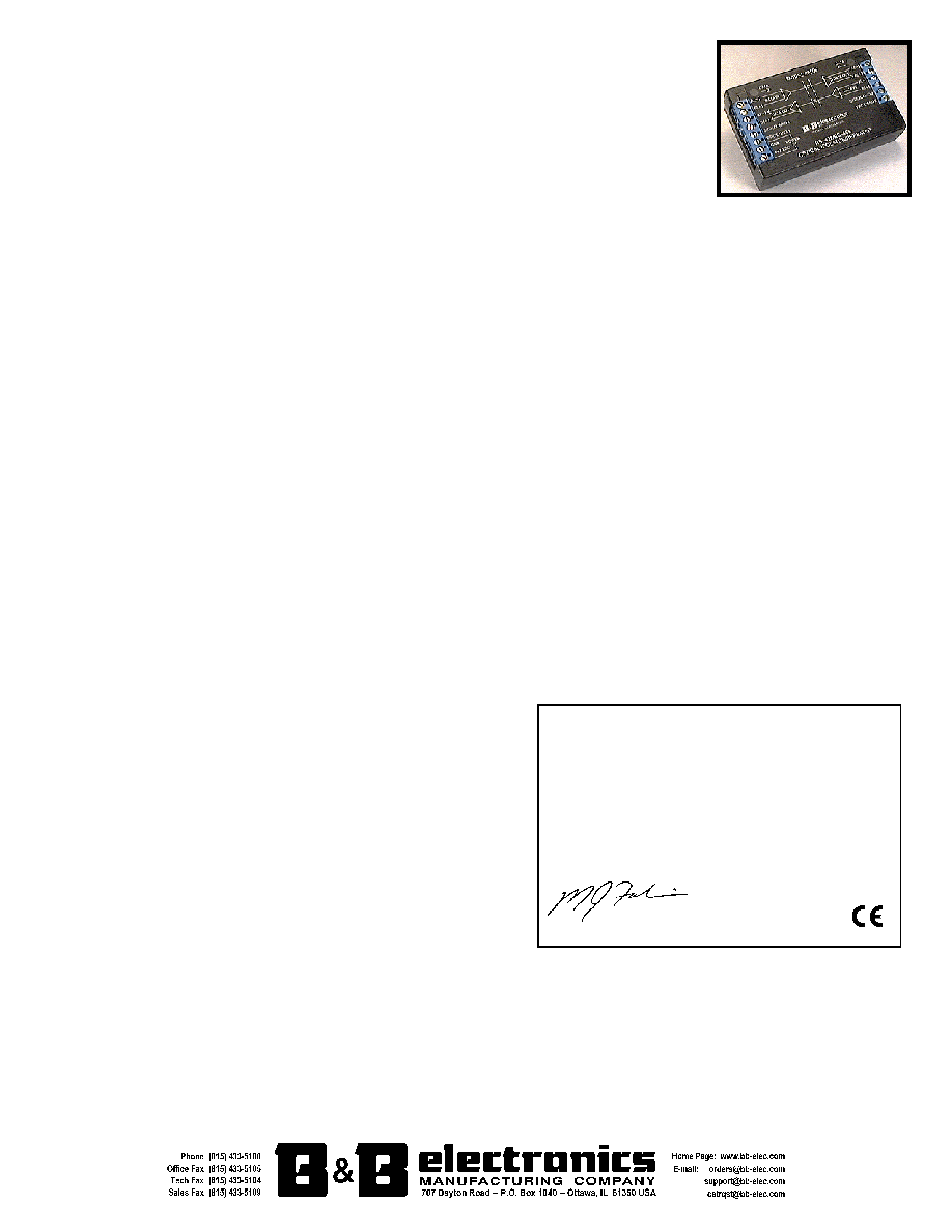
Model 485OP
Description:
The 485OP can be used to optically isolate one piece of RS-485 equipment from the rest of an RS-485 system, or one local group of
RS-485 equipment from another. It can also be used as an RS-485 repeater to expand an existing RS-485 system to greater than the 32
node limitation in the RS-485 Standard. A typical setup using the 485OP as an RS-485 repeater is shown in Figure 1.
All data lines as well as power and ground are isolated from one side of the 485OP to the other. The 485OP uses terminal blocks on
each side of the device. It supports Transmit Data (A) and (B), Receive Data (A) and (B), Protective Ground, and Signal Ground.
Connection:
The 485OP operates in either two-wire half-duplex systems or in four-wire half-duplex or full-duplex systems (see Figures 2 and 3). It
can also operate as a four-wire to two-wire converter. By connecting one side of the 485OP as a two-wire device and one side as a four-
wire device, equipment meant for a point-to-point RS-422 interface can be connected directly to an RS-485 two-wire multi-drop system.
Proper operation of any RS-485 system requires the presence of a signal return path. The RS-485 Standard recommends that a third
wire be used for this. For safety, a 100 ohm resistor should be connected between frame ground and signal ground at every drop point.
For the transient suppression of the 485OP to work properly, the protective ground (PG) terminal must be tied to a good frame (chassis,
green wire, or earth) ground. No wire type or maximum run length is listed in the RS-485 Standard. However, the RS-422 Standard, which
is very similar, recommends number 24AWG twisted pair telephone cable with a shunt capacitance of 16 picofarads per foot and no more
than 4000 feet of distance.
Operation:
When no data is being transmitted through the 485OP, the receivers are enabled on both sides of the device. As data is received on
one side of the 485OP, the opposite driver is enabled and the data traffic LED is turned on. When the 485OP receives the falling edge of
the last data bit, it waits one character time to disable the driver. This timeout period is factory preset for one millisecond to accommodate
a baud rate of 9,600 bits per second. The timeout period can be changed to any value between 0.26 and 4.16 milliseconds by removing
the cover and moving the jumpers JP2 and JP4 inside the 485OP. The preset jumper settings available on the 485OP should
accommodate almost all systems, but a different timeout can be achieved by putting JP2 and JP4 in position E and changing the values of
the capacitors C6 and C9 and resistors R17 and R25. Spaces for through-hole replacement of these components are also provided.
They are labeled C15, C16, R26, and R27. The jumper positions for various baud rates, as well as the resistor and capacitor values for
time-out periods beyond this range are given in Table 1. See Figure 4 for the location of the timing components.
Jumpers JP1 and JP3 determine whether the receivers will be disabled when transmitting (half-duplex) or always enabled (full-
duplex). As a general rule, JP1 and JP3 should be in the half-duplex position for two-wire operation and in the full-duplex position for four-
wire systems. See Figure 4 for the location of jumpers JP1-JP4 on the PC board.
Specifications:
Isolation:
2.000 volts RMS for 1 min. optical isolation of
data lines and ground.
Surge Suppression:
6.5V working peak voltage, bi-directional over
voltage
suppressor.
600W peak power dissipation.
3,000 pF maximum capacitance.
Data Rates:
Up to 460.8K baud.
Temperature Rating: 0
∞
C to +70
∞
C
Power Requirements: 9-14V DC @ 60mA (idle state), 170mA
(Full-duplex data with 62 Ohm load)
Dimensions:
3.8"L x 2.4"W x 1.0"H
FCC Approved Class A
DECLARATION OF CONFORMITY
Manufacturer's Name:
B&B Electronics Manufacturing Company
Manufacturer's Address:
P.O. Box 1040
707 Dayton Road
Ottawa, IL 61350 USA
Model Numbers:
485OP
Description:
RS-485 Optical Isolator/Repeater
Type:
Light industrial ITE equipment
Application of Council Directive:
89/336/EEC
Standards:
EN 50082-1 (IEC 801-3, IEC 801-4)
EN 50081-1 (EN 55022)
EN 61000 (-3-2, -3-3, -4-2, -4-3, -4-4, -4-6, -4-8)
ENV
50204
Michael J. Fahrion, Director of Engineering

Documentation Number 485OP3401- pg. 2/3
© B&B Electronics January 1993 -- Revised August 2001
This product designed and manufactured in USA of domestic and imported parts by
Table 1
APPROXIMATE TIMEOUT VALUES
Baud
Rate
Time
(ms)
Resistor
R17 & R25
(ohm)
Capacitor
C6 & C9
(mfd)
Jumper
Position
JP2 & JP4
300
33.3
330K
0.1
-
600
16.6
160K
0.1
-
1200
8.33
820K
0.01
-
2400
4.16
430K
0.01
A
4800
2.08
200K
0.01
B
9600
1.04
100K
0.01
C
19.2K
0.52
56K
0.01
D
38.4K
0.26
27K
0.01
E
57.6K
0.18
16K
0.01
-
115.2K
0.087
8.2K
0.01
-
FIGURE 1. 485OP As A Two-Wire Repeater
FIGURE 4. PC Board Layout - Top
FIGURE 4. PC Board Layout - Bottom
FIGURE 2. Four-Wire Setup
FIGURE 3. Two-Wire Setup
SIGNAL GROUND
DATA OUT (A)
DATA OUT (B)
SIGNAL GND
TD A (-)
TD B (+)
RD A (-)
RD B (+)
WHITE MARKED WIRE
SOLID BLACK WIRE
485OP
PROT. GROUND
DATA IN (A)
DATA IN (B)
GROUND
+12VDC
SIGNAL GROUND
DATA OUT (A)
DATA OUT (B)
485OP
PROT. GROUND
DATA IN (A)
DATA IN (B)
GROUND
+12VDC
WHITE MARKED WIRE
SOLID BLACK WIRE
SIGNAL GND
DATA B (+)
DATA A (-)
SIG. GROUND
TX/RX A (-)
TX/RX B (+)
HOST DEVICE
FR
AM
E
G
R
O
U
N
D
485 DEVICE
SI
G.
GR
OU
ND
T
X
/R
X B (+)
T
X
/R
X A (-)
UP TO 4000 FT. OF CABLE AND
29 OTHER RS-485 DEVICES
485 DEVICE
SI
G.
G
R
OU
N
D
UP TO 4000 FT. OF CABLE AND
30 OTHER RS-485 DEVICES
485OP
FR
AM
E G
R
O
UND
SIGNAL GROUND
PROT. GROUND
DATA OUT (A)
DATA OUT (B)
SIGNAL GROUND
PROT. GROUND
DATA IN (A)
DATA IN (B)
DATA OUT (A)
DATA OUT (B)
DATA IN (A)
DATA IN (B)
TX
/R
X A
(-)
TX
/R
X B
(+)
+12VDC
GND
+12VDC
GND
FRAME GND
