
2A DDR TERMINATION REGULATOR AP2302L
Preliminary Datasheet
1
Nov. 2005 Rev. 1. 1
BCD Semiconductor Manufacturing Limited
Figure 1. Package Types of AP2302L
General Description
The AP2302L linear regulator is designed to meet the
JEDEC specification SSTL-2 and SSTL-18 for termi-
nation of DDR-SDRAM. The regulator can sink or
source up to 2A current continuously, providing
enough current for most DDR applications. V
OUT
is
designed to track the V
REF
voltage within a
±
20mV
tolerance over the entire current range while prevent-
ing shooting through on the output stage. On-chip ther-
mal limiting provides protection against a combination
of high current and ambient temperature which would
create an excessive junction temperature.
The AP2302L, used in conjunction with series termi-
nation resistors, provides an excellent voltage source
for active termination schemes of high speed transmis-
sion lines as those seen in high speed memory buses
and distributed backplane designs.
The AP2302L is available in SOIC-8 and TO-252-5
packages.
Features
∑
Support Both DDR I (1.25V
TT
) and DDR II
(0.9V
TT
) Requirements
∑
Source and Sink Current up to 2A
∑
High Accuracy Output Voltage at Full-load
∑
Adjustable V
OUT
by External Resistors
∑
Shutdown for Standby or Suspend Mode
Operation with High-impedance Output
Applications
∑
DDR-SDRAM Termination
∑
DDR-II Termination
∑
SSTL-2 Termination
SOIC-8
TO-252-5

2A DDR TERMINATION REGULATOR AP2302L
Preliminary Datasheet
2
Nov. 2005 Rev. 1. 1
BCD Semiconductor Manufacturing Limited
Pin Description
Pin Number
Pin Name
Function
SOIC-8
TO-252-5
1
1
V
IN
Power Input.
2
2
GND
Ground.
3
4
REFEN
Reference Voltage Input and Chip Enable.
4
5
V
OUT
Output Voltage.
5, 6, 7, 8
3
V
CNTL
Supply Voltage for Internal Circuit (Internally Connected for SOIC-8),
(TAB for TO-252-5).
Pin Configuration
Figure 2. Pin Configuration of AP2302L (Top View)
M Package
7 V
CNTL
6 V
CNTL
5 V
CNTL
1
2
3
4
V
IN
GND
REFEN
V
OUT
(SOIC-8)
(TO-252-5)
D Package
V
IN
GND
V
CNTL
(TAB)
REFEN
V
OUT
8 V
CNTL
1
2
3
4
5

2A DDR TERMINATION REGULATOR AP2302L
Preliminary Datasheet
3
Nov. 2005 Rev. 1. 1
BCD Semiconductor Manufacturing Limited
Functional Block Diagram
Figure 3. Functional Block Diagram of AP2302L
Package
Temperature
Range
Part Number
Marking ID
Packing
Type
Tin Lead
Lead Free
Tin Lead
Lead Free
SOIC-8
0 to 125
o
C
AP2302LM-E1
2302LM-E1
Tube
AP2302LMTR-E1
2302LM-E1
Tape Reel
TO-252-5
0 to 125
o
C
AP2302LD-E1
AP2302LD-E1
Tube
AP2302LDTR-E1
AP2302LD-E1
Tape Reel
Ordering Information
BCD Semiconductor's Pb-free products, as designated with "E1" suffix in the part number, are RoHS compliant.
Circuit Type
Package
BANDGAP
START UP
CURRENT
LIMIT
THERMAL
PROTECT
OUTPUT
CONTROL
REFEN
V
IN
V
CNTL
(TAB)
GND
V
OUT
1 (1)
2 (2)
5,6,7,8 (3)
3 (4)
4 (5)
A(B)
A for SOIC-8
B for TO-252-5
M: SOIC-8
D: TO-252-5
AP2302L -
E1: Lead Free
Blank: Tin Lead
TR: Tape and Reel
Blank: Tube

2A DDR TERMINATION REGULATOR AP2302L
Preliminary Datasheet
4
Nov. 2005 Rev. 1. 1
BCD Semiconductor Manufacturing Limited
Absolute Maximum Ratings (Note 1)
Recommended Operating Conditions
Note 1: Stresses greater than those listed under "Absolute Maximum Ratings" may cause permanent damage to the device.
These are stress ratings only, and functional operation of the device at these or any other conditions beyond those indicated
under "Recommended Operating Conditions" is not implied. Exposure to "Absolute Maximum Ratings" for extended periods
may affect device reliability.
Parameter
Symbol
Value
Unit
Supply Voltage for Internal Circuit
V
CNTL
7
V
Power Dissipation
P
D
Internally Limited
W
ESD (Human Body Model)
ESD
2
KV
Storage Temperature Range
T
STG
-65 to 150
o
C
Lead Temperature (Soldering, 5sec)
T
LEAD
260
o
C
Package Thermal Resistance (Free Air)
JC
SOIC-8
28
o
C/W
TO-252-5
13
Parameter
Symbol
Min
Typ
Max
Unit
Supply Voltage for Internal Circuit
V
CNTL
(Note 2, 3)
3.3
6
V
Power Input
DDR I
V
IN
1.6
2.5
V
CNTL
V
DDR II
1.8
Junction Temperature
T
J
0
125
o
C
Note 2: Keep V
CNTL
V
IN
in operation power on and power off sequences.
Note 3: For safe operation, V
CNTL
MUST be tied to 3.3V rather than 5V.
2A DDR TERMINATION REGULATOR AP2302L
Preliminary Datasheet
5
Nov. 2005 Rev. 1. 1
BCD Semiconductor Manufacturing Limited
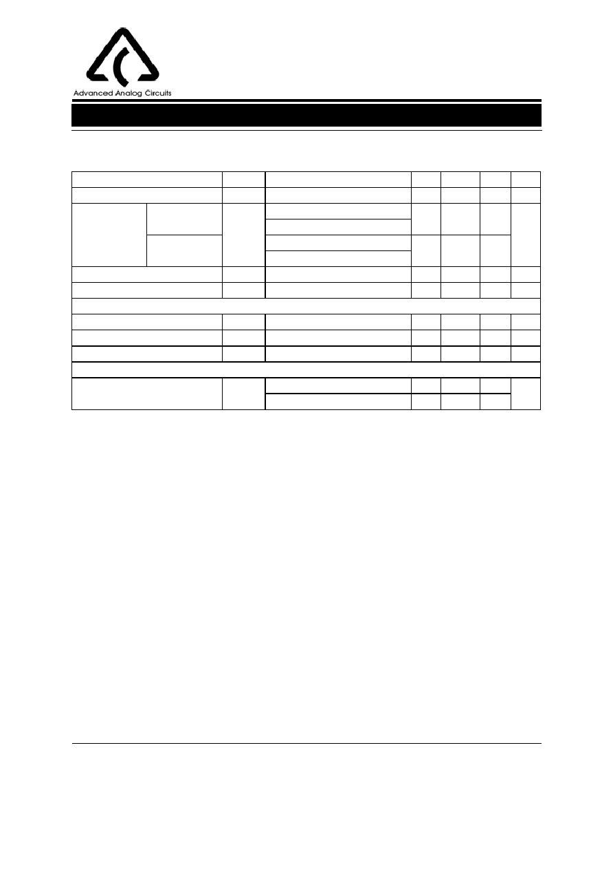
Parameter
Symbol
Conditions
Min
Typ
Max
Unit
Output Offset Voltage
V
OS
L
=0 (Note 4)
-20
0
20
mV
Load
Regulation
DDR I
V
OUT
I
L
=0 to 2A
-20
0
20
mV
I
L
=0 to -2A
DDR II
I
L
=0 to 2A
-20
0
20
I
L
=0 to -2A
Quiescent Current of V
CNTL
I
Q
No Load
3
5
mA
Leakage Current in Shutdown Mode
I
SHDN
V
REFEN
<0.2V, R
L
=180
3
6
µ
A
Protection
Current Limit
I
LIMIT
2.6
A
Thermal Shutdown Temperature
T
SHDN
3.3V
V
CNTL
5V
150
o
C
Thermal Shutdown Hysteresis
50
o
C
Shutdown Function
Shutdown Threshold Trigger
Output=High
0.8
V
Output=Low
0.2
Electrical Characteristics
(T
A
=25
o
C,
V
IN
=2.5V, V
CNTL
=3.3V, V
REFEN
=1.25V, C
OUT
=10
µF (Ceramic), unless otherwise specified.)
Note 4: V
OS
is the voltage measurement defined as V
OUT
subtracted from V
REFEN
.