DUAL OP AMP AND VOLTAGE REFERENCE AP4300
Data Sheet
1
Apr. 2005 Rev. 1. 2
BCD Semiconductor Manufacturing Limited
General Description
The AP4300 is a monolithic IC specifically designed
to regulate the output current and voltage levels of
switching battery chargers and power supplies.
The device contains two operational amplifiers and a
precision shunt regulator. Op Amp 1 is designed for
voltage control, whose non-inverting input internally
connects to the output of the shunt regulator. Op Amp
2 is for current control with both inputs uncommitted.
The IC offers the power converter designer a control
solution that features increased precision with a corre-
sponding reduction in system complexity and cost.
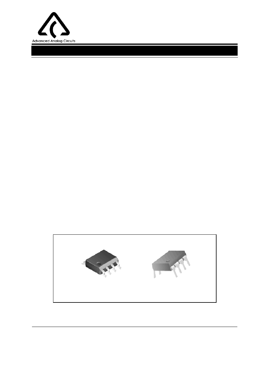
The AP4300 is available in standard packages of DIP-
8 and SOIC-8.
Features
Op Amp
∑
Input Offset Voltage: 0.5mV
∑
Supply Current: 250
µA per Op Amp at 5.0V Sup-
ply Voltage
∑
Unity Gain Bandwidth: 1MHz
∑
Output Voltage Swing: 0 to (V
CC
- 1.5) V
∑
Power Supply Range: 3 to 18V
Voltage Reference
∑
Fixed Output Voltage Reference: 2.5V, 2.6V
∑
Voltage Tolerance: 0.5%, 1%
∑
Sink Current Capability from 0.1 to 80mA
Applications
∑
Battery Charger
∑
Switching Power Supply
Figure 1. Package Types of AP4300
SOIC-8
DIP-8
DUAL OP AMP AND VOLTAGE REFERENCE AP4300
Data Sheet
2
Apr. 2005 Rev. 1. 2
BCD Semiconductor Manufacturing Limited
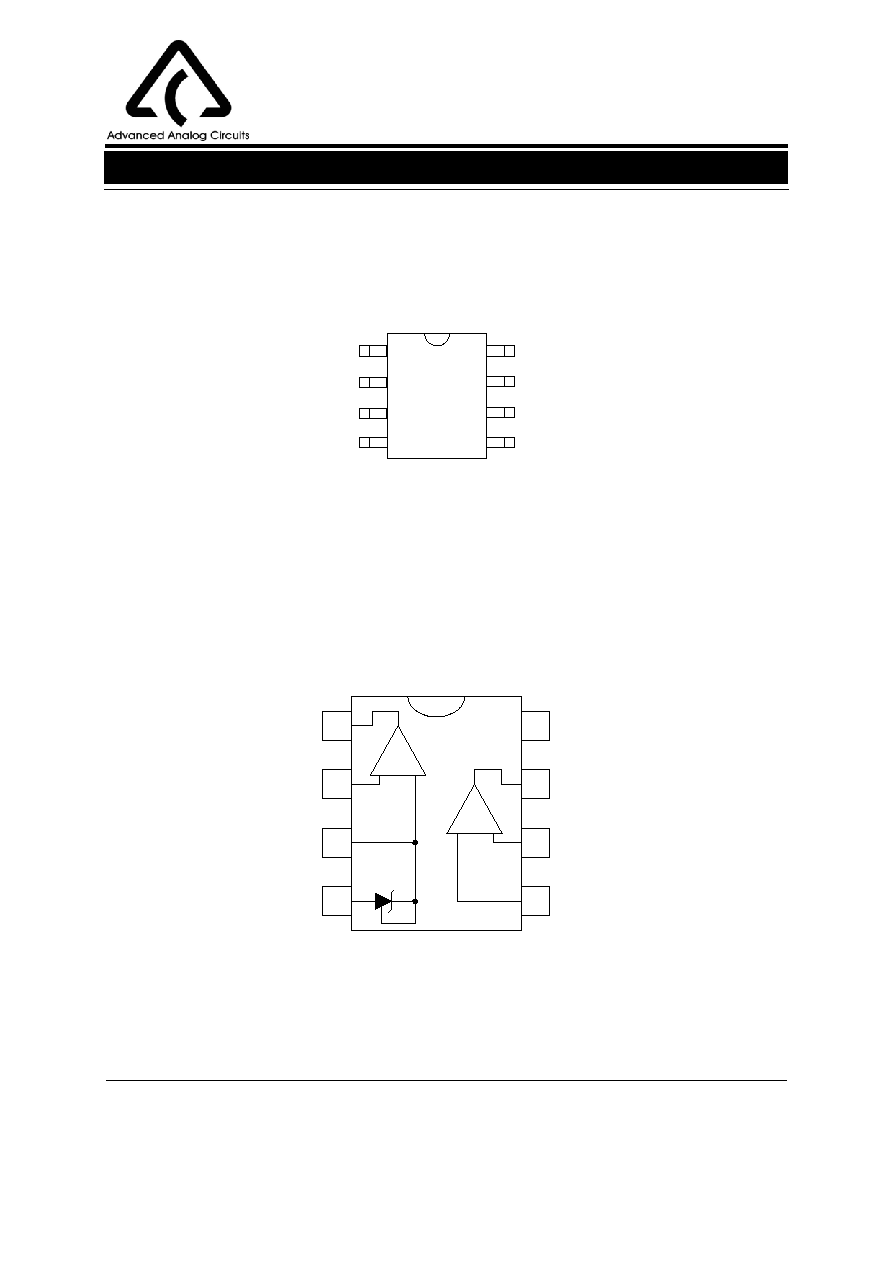
Functional Block Diagram
Figure 2. Pin Configuration of AP4300
INPUT 1-
INPUT 1+ / V
KA
GND
V
CC
OUTPUT 2
INPUT 2-
INPUT 2+
1
4
5
6
7
8
3
2
Top View
OUTPUT 1
Figure 3. Functional Block Diagram of AP4300
-
+
-
+
1
2
3
4
8
7
6
5
OUTPUT 1
INPUT 1
GND
V
CC
OUTPUT 2
INPUT 2
(SOIC-8/DIP-8)
M Package/P Package
Pin Configuration

DUAL OP AMP AND VOLTAGE REFERENCE AP4300
Data Sheet
3
Apr. 2005 Rev. 1. 2
BCD Semiconductor Manufacturing Limited
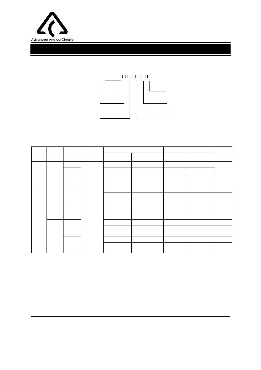
Figure 5. Voltage Reference Functional Block Diagram
Functional Block Diagram (Continued)
Figure 4. Op Amp Functional Block Diagram
(Each Amplifier)
V
KA
GND
20
µ
A
20
µ
A
Q2
Q4
Q3
Q1
Q8
Q9
6
µ
A
4
µ
A
Q10
Q11
50
µ
A
Q5
Q6
Q13
Rsc
Cc
100
µ
A
Q7
INPUT-
INPUT+
OUTPUT
Q12
V
CC
DUAL OP AMP AND VOLTAGE REFERENCE AP4300
Data Sheet
4
Apr. 2005 Rev. 1. 2
BCD Semiconductor Manufacturing Limited
Package
Refer-
ence
Voltage
Voltage
Tolerance
Tempera-
ture Range
Part Number
Marking ID
Packing
Type
Tin Lead
Lead Free
Tin Lead
Lead Free
DIP-8
2.6V
0.5%
-40 to 105
o
C
AP4300AP-A
AP4300AP-AE1
AP4300AP-A
AP4300AP-AE1
Tube
1%
AP4300BP-A
AP4300BP-AE1
AP4300BP-A
AP4300BP-AE1
2.5V
0.5%
AP4300AP-B
AP4300AP-BE1
AP4300AP-B
AP4300AP-BE1
1%
AP4300BP-B
AP4300BP-BE1
AP4300BP-B
AP4300BP-BE1
SOIC-8
2.6V
0.5%
-40 to 105
o
C
AP4300AM-A
AP4300AM-AE1
AP4300AM-A AP4300AM-AE1
Tube
AP4300AM-ATR AP4300AM-ATRE1 AP4300AM-A AP4300AM-AE1
Tape &
Reel
1%
AP4300BM-A
AP4300BM-AE1
AP4300BM-A AP4300BM-AE1
Tube
AP4300BM-ATR AP4300BM-ATRE1 AP4300BM-A AP4300BM-AE1
Tape &
Reel
2.5V
0.5%
AP4300AM-B
AP4300AM-BE1
AP4300AM-B AP4300AM-BE1
Tube
AP4300AM-BTR AP4300AM-BTRE1 AP4300AM-B AP4300AM-BE1
Tape &
Reel
1%
AP4300BM-B
AP4300BM-BE1
AP4300BM-B AP4300BM-BE1
Tube
AP4300BM-BTR AP4300BM-BTRE1 AP4300BM-B AP4300BM-BE1
Tape &
Reel
Circuit Type
Voltage Tolerance
A: 0.5%
B: 1%
Package
P: DIP-8
M: SOIC-8
Output Voltage Reference
A: 2.6V
B: 2.5V
BCD Semiconductor's Pb-free products, as designated with "E1" suffix in the part number, are RoHS compliant.
AP4300 -
E1: Lead-free
Blank: Tin Lead
TR: Tape and Reel
Blank: Tube
Ordering Information
DUAL OP AMP AND VOLTAGE REFERENCE AP4300
Data Sheet
5
Apr. 2005 Rev. 1. 2
BCD Semiconductor Manufacturing Limited
Parameter
Symbol
Value
Unit
Power Supply Voltage (V
CC
to GND)
V
CC
20
V
Op Amp 1 and 2 Input Voltage Range (Pins 2, 5, 6)
V
IN
- 0.3 to V
CC
+ 0.3
V
Op Amp 2 Input Differential Voltage (Pins 5, 6)
V
ID
20
V
Voltage Reference Cathode Current (Pin 3)
I
K
100
mA
Power Dissipation
P
D
DIP-8
800
mW
SOIC-8
500
Storage Temperature Range
T
STG
-65 to 150
o
C
ESD Protection Voltage (Machine Model)
> 200
V
Note 1: Stresses greater than those listed under "Absolute Maximum Ratings" may cause permanent damage to the
device. These are stress ratings only, and functional operation of the device at these or any other conditions beyond
those indicated under "Recommended Operating Conditions" is not implied. Exposure to "Absolute Maximum
Ratings" for extended periods may affect device reliability.
Parameter
Min
Max
Unit
Supply Voltage
3
18
V
Ambient Temperature
-40
105
o
C
Recommended Operating Conditions
Absolute Maximum Ratings (Note 1)