
DUAL OPAMP AND VOLTAGE REFERENCE AP4301
1
March, 2003
Advanced Analog Circuits
Data Sheet
Rev.1.0
General Description
The AP4301 is a monolithic IC specifically designed
to control the output current and voltage levels of
switch mode battery chargers and power supplies.
The device contains two operational amplifiers and a
precision shunt regulator. OPAMP 1 is designed for
voltage control, whose non-inverting input internally
connects to the ouput of the shunt regulator. OPAMP 2
is for current control with both inputs uncommitted.
The IC offers the power converter designer a control
solution that features increased precision with a corre-
sponding reduction in system complexity and cost.
Features
∑
Input offset voltage: 0.5mV
∑
Supply current: 250
µA per Op-Amp at 5.0V sup-
ply voltage
∑
Unity gain bandwidth: 1MHz
∑
Output voltage swing: 0 to (V
CC
- 1.5)V
∑
Power supply range: 3 to 18V
∑
Fixed output voltage reference: 1.25V, 1.24V
∑
Voltage tolerance: 0.5%, 1%
∑
Sink current capability from 0.1 to 80mA
∑
Package types: DIP-8 and SOIC-8
Applications
∑
Battery charger
∑
Switch mode power supply
SOIC-8
DIP-8
Figure 1. Package Types of AP4301

DUAL OPAMP AND VOLTAGE REFERENCE AP4301
2
March, 2003
Advanced Analog Circuits
Data Sheet
Rev.1.0
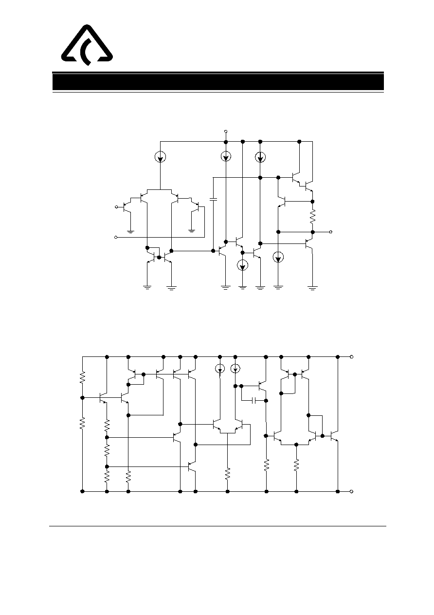
Functional Block Diagram
Pin Configuration
Figure 2. Pin configuration of AP4301
INPUT 1-
INPUT 1+ / V
KA
GND
V
CC
OUTPUT 2
INPUT 2-
INPUT 2+
1
4
5
6
7
8
3
2
Top View
OUTPUT 1
Figure 3. Functional Block Diagram of AP4301
-
+
-
+
1
2
3
4
8
7
6
5
OUTPUT 1
INPUT 1
GND
V
CC
OUTPUT 2
INPUT 2
DUAL OPAMP AND VOLTAGE REFERENCE AP4301
3
March, 2003
Advanced Analog Circuits
Data Sheet
Rev.1.0
Figure 5. Voltage Reference Functional Block Diagram
Functional Block Diagram (Continued)
Figure 4. OPAMP Functional Block Diagram
V
KA
GND
20
µA
20
µA
6uA
4uA
Rsc
100uA
INPUTS
+
-
OUTPUT
V
CC
10
µA
50µA
GND
(Each Amplifier)

DUAL OPAMP AND VOLTAGE REFERENCE AP4301
4
March, 2003
Advanced Analog Circuits
Data Sheet
Rev.1.0
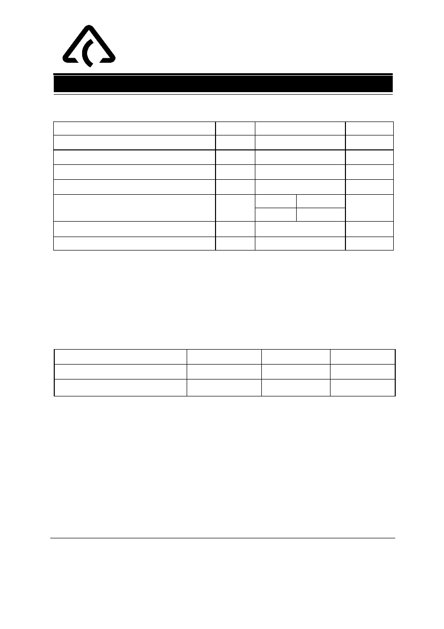
Ordering Information
Package
Reference
Voltage
Voltage
Tolerance
Temperature
Range
Part Number
Marking ID
Packing Type
DIP-8
1.25V 0.5%
-40 to 85
o
C
AP4301AP-C
AP4301AP-C
Tube
1%
AP4301BP-C
AP4301BP-C
1.24V
0.5%
AP4301AP-D
AP4301AP-D
1%
AP4301BP-D
AP4301BP-D
SOIC-8
1.25V
0.5%
AP4301AM-C
AP4301AM-C
Tube/Reel
1%
AP4301BM-C
AP4301BM-C
1.24V
0.5%
AP4301AM-D
AP4301AM-D
1%
AP4301BM-D
AP4301BM-D
AP 4301 X X - X
Output Voltage Reference
C: 1.25V
D: 1.24V
Circuit Type
Voltage Tolerence
A:0.5%
B:1%
Package
M:SOIC-8
P: DIP-8
DUAL OPAMP AND VOLTAGE REFERENCE AP4301
5
March, 2003
Advanced Analog Circuits
Data Sheet
Rev.1.0
Parameter
Symbol
Value
Unit
Power Supply Voltage (V
CC
to GND)
V
CC
20
V
OPAMP 1 and 2 Input Voltage Range (Pins 2, 5, 6)
V
IN
- 0.3 to V
CC
- 0.3
V
OPAMP 2 Input Differential Voltage (Pins 5, 6)
V
ID
20
V
Voltage Reference Cathode Current (Pin 3)
I
K
100
mA
Power Dissipation
P
D
DIP-8
800
mW
SOIC-8
500
Storage Temperature Range
T
STG
-65 to 150
o
C
ESD Protection Voltage (Machine Model)
-
200
V
Absolute Maximum Ratings
Note: Stresses greater than those listed under "Absolute Maximum Ratings " may cause permanent damage to the
device. These are stress ratings only, and functional operation of the device at these or any other conditions beyond
those indicated under "Recommended Operation Ratings " is not implied. Exposure to "Absolute Maximum Rat-
ings " for extended periods may affect device reliability.
Parameter
Min
Max
Unit
Supply Voltage
3
18
V
Ambient Temperature
-40
85
o
C
Recommended Operating Ratings

DUAL OPAMP AND VOLTAGE REFERENCE AP4301
6
March, 2003
Advanced Analog Circuits
Data Sheet
Rev.1.0
Operating Conditions: V
CC
=
+
5V, T
A
= 25
o
C unless otherwise specified.
Electrical Characteristics
Parameter
Conditions
Min
Typ
Max
Unit
Total Supply Current, excluding Cur-
rent in Voltage Reference
V
CC
= 5V, no load, -40
o
C
T
A
85
o
C
0.5
0.8
mA
V
CC
= 18V, no load, -40
o
C
T
A
85
o
C
0.6
1.2
Voltage Reference Section
Refeence Voltage for AP4301-C
I
K
= 10mA
T
A
= 25
o
C
0.5% tolerance
1.244 1.250
1.256
V
1% tolerance
1.237
1.263
Reference Voltage for AP4301- D
I
K
= 10mA
T
A
= 25
o
C
0.5% tolerance
1.234 1.240
1.246
V
1% tolerance
1.227
1.252
Reference Voltage Deviation
Over Full Temperature Range
I
K
= 10mA, T
A
= -40 to 85
o
C
5
17
mV
Minimum Cathode Current
for Regulation
0.2
1
mA
Dynamic Impedance
I
K
= 1.0 to 80mA, f<1kHz
0.2
0.5
OPAMP 1 Section (V
CC
= 5V, V
O
= 1.4V, T
A
= 25
o
C, unless otherwise noted)
Input Offset Voltage
T
A
= 25
o
C
0.5
3
mV
T
A
= -40 to 85
o
C
5
Input Offset Voltage
Temperature Drift
T
A
= -40 to 85
o
C
7
µV/
o
C
Input Bias Current (Inverting Input
Only)
T
A
= 25
o
C
20
150
nA
Large Signal Voltage Gain
V
CC
= 15V, R
L
= 2K
, V
O
= 1.4 to 11.4V
85
100
dB
Power Supply Rejection Ratio
V
CC
= 5 to 18V
70
90
dB
Output Current
Source
V
CC
= 15V, V
ID
= 1V, V
O
=2V
20
40
mA
Sink
V
CC
= 15V, V
ID
= -1V, V
O
= 2V
10
20
mA
Output Voltage Swing (High)
V
CC
= 18V, R
L
= 10K
, V
ID
= 1V
16
16.5
V
Output Voltage Swing (Low)
V
CC
= 18V, R
L
= 10K
, V
ID
= -1V
17
100
mV
Slew Rate
V
CC
= 18V, R
L
= 2k
, A
V
= 1,
V
IN
= 0.5 to 2V, C
L
= 100pF
0.2
0.5
V/
µ s
Gain Bandwidth Product
V
CC
= 18V, R
L
= 2k
, C
L
= 100pF,
V
IN
= 10mV, f = 100kHz
0.5
1
MHz

DUAL OPAMP AND VOLTAGE REFERENCE AP4301
7
March, 2003
Advanced Analog Circuits
Data Sheet
Rev.1.0
Parameter
Conditions
Min
Typ
Max
Unit
OPAMP2 Section (V
CC
= 5V, V
O
= 1.4V, T
A
= 25
o
C, unless otherwise noted )
Input Offset Voltage
T
A
= 25
o
C
0.5
3
mV
T
A
= -40 to 85
o
C
5
Input Offset Voltage Temperature
Drift
T
A
= -40 to 85
o
C
7
µV/
o
C
Input Offset Current
T
A
= 25
o
C
2
30
nA
Input Bias Current
T
A
= 25
o
C
20
150
nA
Input Voltage Range
V
CC
= 0 to 18V
0
V
CC
- 1.5
V
Common Mode Rejection Ratio
T
A
= 25
o
C, V
CM
= 0 to 3.5V
70
85
dB
Large Signal Voltage Gain
V
CC
= 15V, R
L
= 2k
, V
O
= 1.4 to 11.4V 85
100
dB
Power Supply Rejection Ratio
V
CC
= 5 to 18V
70
90
d
Output Current
Source
V
CC
= 15V , V
ID
= 1V, V
O
= 2V
20
40
mA
Sink V
CC
= 15V, V
ID
= -1V, V
O
= 2V
10
20
mA
Output Voltage Swing ( High )
V
CC
= 18 , R
L
= 10k
, V
ID
= 1V
16
16.5
V
Output Voltage SWing ( Low )
V
CC
= 18 , R
L
= 10k
, V
ID
= -1V
17
100
mV
Slew Rate
V
CC
= 18V, R
L
= 2k
, A
V
= 1,
V
IN
= 0.5 to 2V , C
L
= 100pF
0.2
0.5
V/
µ s
Gain Bandwidth Product
V
CC
= 18V, R
L
= 2k
, C
L
= 100pF,
V
IN
= 10mV, f=100kHz
0.5
1
MHz
Electrical Characteristics (Continued)
Operating Conditions: V
CC
=
+
5V, T
A
= 25
o
C unless otherwise specified.

DUAL OPAMP AND VOLTAGE REFERENCE AP4301
8
March, 2003
Advanced Analog Circuits
Data Sheet
Rev.1.0
Typical Characteristics
Figure 6. Reference Voltage vs. Ambient Temperature
Figure 8. Cathode Current vs. Cathode Voltage
Figure 9. Cathode Current vs. Cathode Voltage
-40
-20
0
20
40
60
80
100
120
1.246
1.248
1.250
1.252
1.254
R
e
fe
re
nc
e V
o
lt
a
g
e
(V
)
Amibient Temperature (
o
C)
AP4301-C
Figure 7. Reference Voltage vs. Ambient Temperature
-1
0
1
-150
-100
-50
0
50
100
150
Ca
t
hode
Current (m
A)
Cathode Voltage (V)
AP4301-D
V
KA
=V
REF
T
A
=25
o
C
-1
0
1
-150
-100
-50
0
50
100
150
Ca
t
hode
Current (m
A)
Cathode Voltage (V)
AP4301-C
V
KA
=V
REF
T
A
=25
o
C
-40
-20
0
20
40
60
80
100
120
1.230
1.232
1.234
1.236
1.238
1.240
1.242
1.244
R
e
fe
re
nc
e V
o
lt
a
g
e
(V
)
Amibient Temperature (
o
C)
AP4301-D

DUAL OPAMP AND VOLTAGE REFERENCE AP4301
9
March, 2003
Advanced Analog Circuits
Data Sheet
Rev.1.0
Typical Characteristics (Continued)
-40
-20
0
20
40
60
80
100
120
0
5
10
15
20
25
30
I
n
p
u
t
B
i
as Cur
r
ent
(
n
A)
Ambient Temperature (
o
C)
0
2
4
6
8
10
12
14
16
18
20
60
70
80
90
100
110
Vol
t
ag
e Gai
n
(d
B)
Supply Voltage (V)
R
L
=2K
R
L
=20K
Figure10. Input Bias Current vs. Ambient Temperature
Figure 11. Operational Amplifier Voltage Gain

DUAL OPAMP AND VOLTAGE REFERENCE AP4301
10
March, 2003
Advanced Analog Circuits
Data Sheet
Rev.1.0
Typical Application
Figure 12. Typical Application of AP4301
AC
Line
SMPS
R2
Current
Sense
R7
R8
Battery
Pack
+
-
+
-
R4
R3
OPAMP 2
OPAMP 1
V
REF
R5
R6
R1
Opto
Isolator
AP4301
7
5
6
4
2
3
1
8

DUAL OPAMP AND VOLTAGE REFERENCE AP4301
11
March, 2003
Advanced Analog Circuits
Data Sheet
Rev.1.0
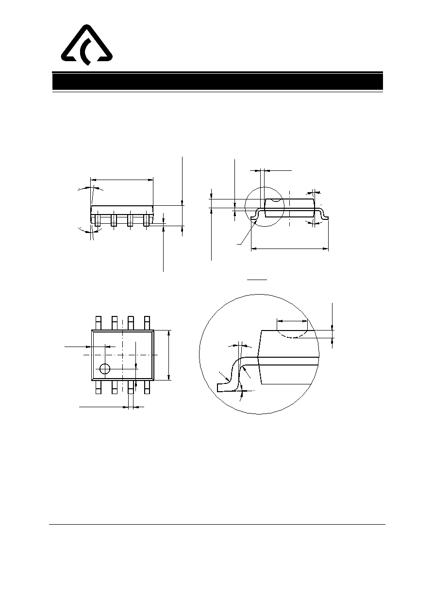
Mechanical Dimensions
DIP - 8
4∞
6∞
R0.75
6
.
6
0
±
0
.
5
0
0.457
0.254
0.13MIN
2.54
10.0MAX
0.28±0.07
1.46±0.31
7.62±0.25
4∞
6∞
5∞
3
.
3
0
±
0
.
3
0
9.2±0.10
3◊0.15±0.05
0.7
DUAL OPAMP AND VOLTAGE REFERENCE AP4301
12
March, 2003
Advanced Analog Circuits
Data Sheet
Rev.1.0
SOIC - 8
Mechanical Dimensions (Continued)
8∞
D
±4∞
4∞
3∞
±2∞
R0.15
R0.15
1.00
0.42±0.09
4.9±0.10
1
.
5
5
±
0
.
2
0
0
.
2
±
0
.
1
0
0
.
9
0
0.8
6.00±0.20
0
.
2
2
±
0
.
0
3
0
.
7
0
±
0
.
0
2
5
0.32
0
.
2
0
3
.
9
0
±
0
.
1
0
7∞
7∞
8∞
20:1
D

IA LOW DROPOUT LINEAR REGULATOR AZ1117
Advanced Analog Circuits
http://www.aacmicro.com
USA:
1510 Montague Expressway, San Jose, CA 95131, USA Tel: 408-433-9888, Fax: 408-432-9888
China:
8th Floor, Zone B, 900 Yi Shan Road, Shanghai 200233, China Tel: 86-21-6495-9539, Fax: 86-21-6485-9673
Taiwan:
Room 2210, 22nd Fl, 333, Keelung Road, Secretary 1, Taipei, Taiwan Tel: 886-2-2564-3699, Fax: 886-2-2564-3770
IMPORTANT NOTICE
Advanced Analog Circuits Corporation reserves the right to make changes to its products or specifications at any time, without
notice, to improve design or performance and to supply the best possible product. Advanced Analog Circuits does not assume any
responsibility for use of any circuitry described other than the circuitry embodied in Advanced Analog Circuits' products. The
company makes no representation that circuitry described herein is free from patent infringement or other rights of Advanced
Analog Circuits Corporation.