
QUAD OP AMP AND VOLTAGE REFERENCE AP4303
Data Sheet
1
Apr. 2005 Rev. 1. 1
BCD Semiconductor Manufacturing Limited
General Description
The AP4303 is a monolithic IC that contains quad
operational amplifiers and a precision shunt regulator,
1.25Vfor AP4303-C or 1.24V for AP4303-D respec-
tively. It is specifically designed to regulate the output
current and voltage levels of switching battery charg-
ers and power supplies.
The four Op Amps feature accurate voltage and current
control. Combining a stable voltage reference with the
four Op Amps makes AP4303 ideal for use in multi-
function charger, power supply voltage monitor, signal
processing and control system.
The IC offers the power converter designer a control
solution that features increased precision with a corre-
sponding reduction in system complexity and cost.
The AP4303 is available in standard packages of DIP-
16 and SOIC-16.
Features
Op Amp
∑
Input Offset Voltage: 0.5mV
∑
Supply Current: 250
µA per Op Amp at 5.0V Sup-
ply Voltage
∑
Unity Gain Bandwidth: 1MHz
∑
Output Voltage Swing: 0 to (V
CC
- 1.5)V
∑
Power Supply Range: 3 to 18V
Voltage Reference
∑
Reference Voltage Tolerance: 0.5%, 1%
∑
Sink Current Capability from 0.1 to 80mA
∑
Output Dynamic Impedance: 0.2
∑
Externally Adjusted Output Voltage Reference:
1.25V for AP4303-C and 1.24V for AP4303-D
Applications
∑
Battery Charger
∑
Switching Power Supply
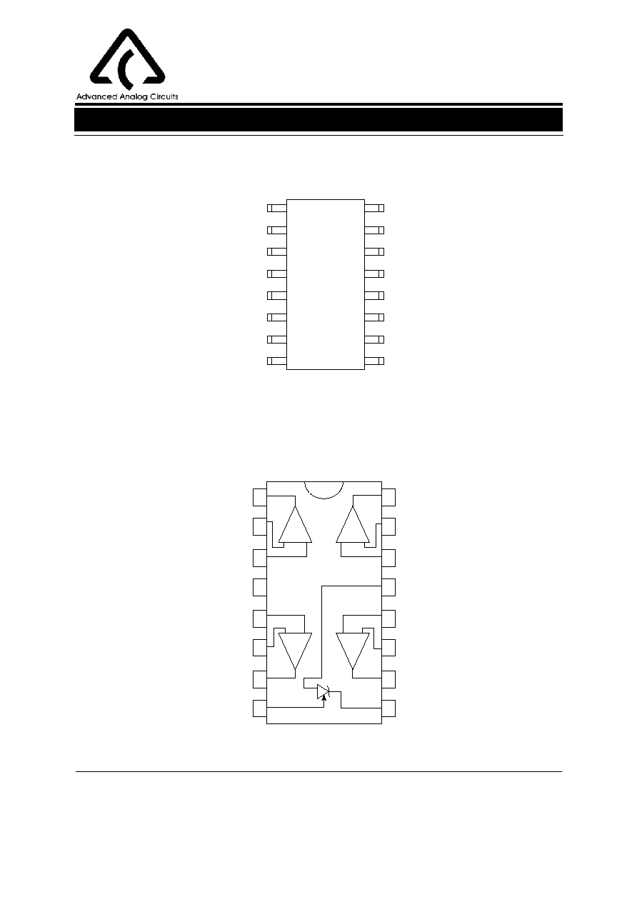
Figure 1. Package Types of AP4303
SOIC-16
DIP-16
QUAD OP AMP AND VOLTAGE REFERENCE AP4303
Data Sheet
2
Apr. 2005 Rev. 1. 1
BCD Semiconductor Manufacturing Limited
Functional Block Diagram
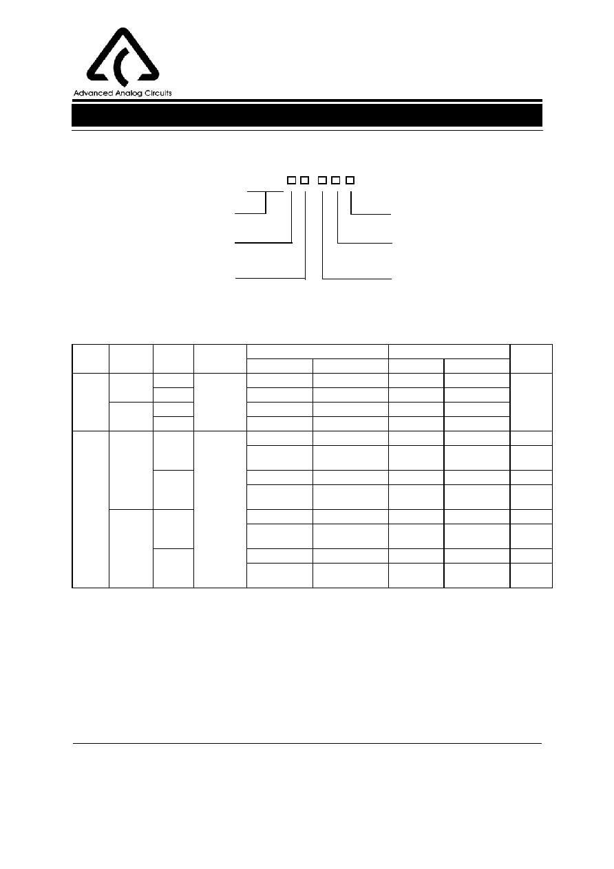
Pin Configuration
Figure 2. Pin configuration of AP4303
INPUT 1-
INPUT 1+
V
CC
OUTPUT 4
INPUT 4-
INPUT 4+
GND
Top View
OUTPUT 1
INPUT 2+
INPUT 2-
OUTPUT 2
V
REF
INPUT 3+
INPUT 3-
OUTPUT 3
CATHODE
1
2
3
4
5
6
7
8
16
15
14
13
12
11
10
9
Figure 3. Functional Block Diagram of AP4303
-
+
-
-
-
+
+
+
OUTPUT 4
INPUT 4-
INPUT 4+
GND
CATHODE
OUTPUT 3
INPUT 3-
INPUT 3+
V
REF
OUTPUT 2
INPUT 2-
INPUT 2+
V
CC
INPUT 1+
INPUT 1-
OUTPUT 1
1
2
3
4
5
6
7
8
16
15
14
13
12
11
10
9
(SOIC-16/DIP-16)
M Package/P Package

QUAD OP AMP AND VOLTAGE REFERENCE AP4303
Data Sheet
3
Apr. 2005 Rev. 1. 1
BCD Semiconductor Manufacturing Limited
Figure 5. Voltage Reference Functional Block Diagram
Functional Block Diagram (Continued)
Figure 4. Op Amp Functional Block Diagram
(Each Amplifier)
CATHODE
GND
V
REF
20
µ
A
20
µ
A
Q2
Q4
Q3
Q1
Q8
Q9
6
µ
A
4
µ
A
Q10
Q11
50uA
Q5
Q6
Q13
Rsc
Cc
100
µ
A
Q7
INPUT-
INPUT+
OUTPUT
Q12
V
CC
QUAD OP AMP AND VOLTAGE REFERENCE AP4303
Data Sheet
4
Apr. 2005 Rev. 1. 1
BCD Semiconductor Manufacturing Limited
Circuit Type
Voltage Tolerance
A: 0.5%
B: 1%
Package
P: DIP-16
M: SOIC-16
Output Voltage Reference
C: 1.25V
D: 1.24V
AP4303 -
E1: Lead Free
Blank: Tin Lead
TR: Tape and Reel
Blank: Tube
Package
Reference
Voltage
Voltage
Tolerance
Tempera-
ture Range
Part Number
Marking ID
Packing
Type
Tin Lead
Lead Free
Tin Lead
Lead Free
DIP-16
1.25V
0.5%
-40 to 85
o
C
AP4303AP-C
AP4303AP-CE1
AP4303AP-C
AP4303AP-CE1
Tube
1%
AP4303BP-C
AP4303BP-CE1
AP4303BP-C
AP4303BP-CE1
1.24V
0.5%
AP4303AP-D
AP4303AP-DE1
AP4303AP-D
AP4303AP-DE1
1%
AP4303BP-D
AP4303BP-DE1
AP4303BP-D
AP4303BP-DE1
SOIC-16
1.25V
0.5%
-40 to 85
o
C
AP4303AM-C
AP4303AM-CE1
AP4303AM-C AP4303AM-CE1
Tube
AP4303AM-CTR AP4303AM-CTRE1 AP4303AM-C AP4303AM-CE1
Tape &
Reel
1%
AP4303BM-C
AP4303BM-CE1
AP4303BM-C AP4303BM-CE1
Tube
AP4303BM-CTR AP4303BM-CTRE1 AP4303BM-C AP4303BM-CE1
Tape &
Reel
1.24V
0.5%
AP4303AM-D
AP4303AM-DE1
AP4303AM-D AP4303AM-DE1
Tube
AP4303AM-DTR AP4303AM-DTRE1 AP4303AM-D AP4303AM-DE1
Tape &
Reel
1%
AP4303BM-D
AP4303BM-DE1
AP4303BM-D AP4303BM-DE1
Tube
AP4303BM-DTR AP4303BM-DTRE1 AP4303BM-D AP4303BM-DE1
Tape &
Reel
BCD Semiconductor's Pb-free products, as designated with "E1" suffix in the part number, are RoHS compliant.
Ordering Information
QUAD OP AMP AND VOLTAGE REFERENCE AP4303
Data Sheet
5
Apr. 2005 Rev. 1. 1
BCD Semiconductor Manufacturing Limited
Parameter
Min
Max
Unit
Supply Voltage
3
18
V
Ambient Temperature
-40
85
o
C
Recommended Operating Conditions
Note 1: Stresses greater than those listed under "Absolute Maximum Ratings " may cause permanent damage to
the device. These are stress ratings only, and functional operation of the device at these or any other conditions
beyond those indicated under "Recommended Operating Conditions" is not implied. Exposure to "Absolute Max-
imum Ratings " for extended periods may affect device reliability.
Parameter Symbol
Value
Unit
Power Supply Voltage (V
CC
to GND)
V
CC
20
V
Op Amp Input Voltage Range
V
IN
-0.3 to V
CC
+ 0.3
V
Op Amp Input Differentials Voltage
V
ID
20
V
Voltage Reference Cathode Current (Pin 9)
I
K
100
mA
Power Dissipation
DIP-16
P
D
1000
mW
SOIC-16
1000
Storage Temperature Range
T
STG
-65 to 150
o
C
ESD Protection Voltage (Machine Model)
>200
V
Absolute Maximum Ratings (Note 1)