 | –≠–ª–µ–∫—Ç—Ä–æ–Ω–Ω—ã–π –∫–æ–º–ø–æ–Ω–µ–Ω—Ç: AP4310AP | –°–∫–∞—á–∞—Ç—å:  PDF PDF  ZIP ZIP |

DUAL OP AMP AND VOLTAGE REFERENCE AP4310
Preliminary Datasheet
1
Apr. 2005 Rev. 1. 2
BCD Semiconductor Manufacturing Limited
General Description
The AP4310 is a monolithic IC specifically designed
to regulate the output current and voltage levels of
switching battery chargers and power supplies.
The device contains two Op Amps and a 2.5V preci-
sion shunt voltage reference. Op Amp 1 is designed for
voltage control with its non-inverting input internally
connects to the output of the shunt regulator. Op Amp
2 is for current control with both inputs uncommitted.
The IC offers the power converter designer a control
solution that features increased precision with a corre-
sponding reduction in system complexity and cost.
The AP4310 is available in standard packages of DIP-
8 and SOIC-8.
Features
Op Amp
∑
Input Offset Voltage: 0.5mV
∑
Supply Current: 75
µA per Op Amp at 5.0V Sup-
ply Voltage
∑
Unity Gain Bandwidth: 1MHz
∑
Output Voltage Swing: 0 to (V
CC
- 1.5) V
∑
Power Supply Range: 3 to 36V
Voltage Reference
∑
Fixed Output Voltage Reference: 2.5V
∑
Voltage Tolerance:
± 0.4%, ± 1%
∑
Sink Current Capability: 0.05 to 80mA
∑
Typical Output Impedance: 0.2
Applications
∑
Battery Charger
∑
Switching Power Supply
Figure 1. Package Types of AP4310
SOIC-8
DIP-8

DUAL OP AMP AND VOLTAGE REFERENCE AP4310
Preliminary Datasheet
2
Apr. 2005 Rev. 1. 2
BCD Semiconductor Manufacturing Limited
Functional Block Diagram
Pin Configuration
Figure 2. Pin Configuration of AP4310
INPUT 1-
INPUT 1+ / V
KA
GND
V
CC
OUTPUT 2
INPUT 2-
INPUT 2+
1
4
5
6
7
8
3
2
OUTPUT 1
Figure 3. Functional Block Diagram of AP4310
V
CC
OUTPUT 2
INPUT 2-
INPUT 2+
GND
INPUT 1+ / V
KA
INPUT 1-
OUTPUT 1
(SOIC-8/DIP-8)
M Package/P Package
Top View
-
+
-
+
1
2
3
4
8
7
6
5
Op
Amp 1
Op
Amp 2

DUAL OP AMP AND VOLTAGE REFERENCE AP4310
Preliminary Datasheet
3
Apr. 2005 Rev. 1. 2
BCD Semiconductor Manufacturing Limited
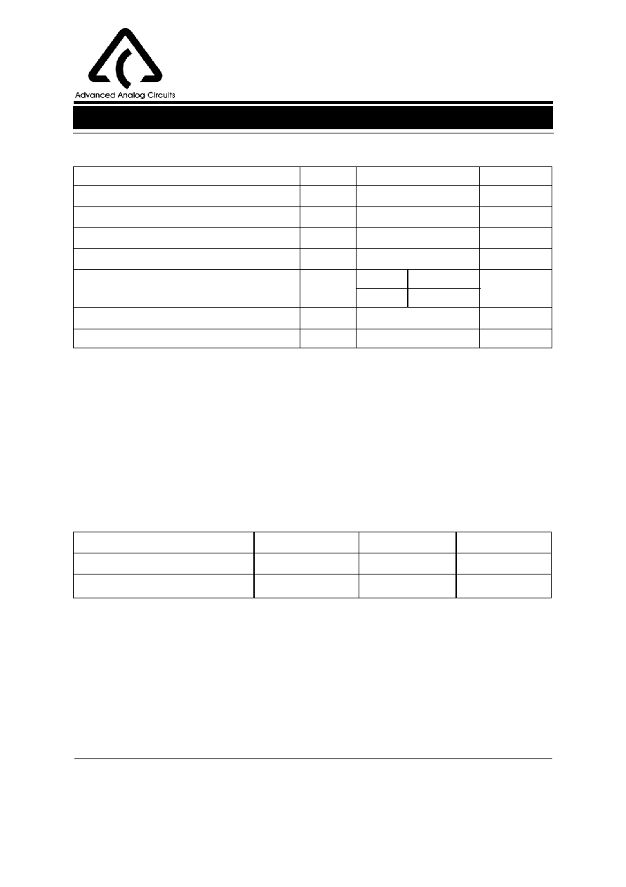
AP4310 -
Package
Reference
Voltage
Voltage
Tolerance
Tempera-
ture Range
Part Number
Marking ID
Packing
Type
Tin Lead
Lead Free
Tin Lead
Lead Free
DIP-8
2.5V
±
0.4%
-40 to105
o
C
AP4310AP
AP4310AP-E1
AP4310AP
AP4310AP-E1
Tube
±
1%
AP4310P
AP4310P-E1
AP4310P
AP4310P-E1
SOIC-8
2.5V
±
0.4%
-40 to105
o
C AP4310AM
AP4310AM-E1
4310AM
AP4310AM-E1
Tube
AP4310AMTR AP4310AMTR-E1
4310AM
AP4310AM-E1 Tape & Reel
±
1%
-40 to105
o
C AP4310M
AP4310M-E1
4310M
AP4310M-E1
Tube
AP4310MTR
AP4310MTR-E1
4310M
AP4310M-E1
Tape & Reel
Circuit Type
Voltage Tolerance
A:
± 0.4%
Blank:
± 1%
Package
P: DIP-8
M: SOIC-8
E1: Lead Free
Blank: Tin Lead
TR: Tape and Reel
Blank: Tube
BCD Semiconductor's Pb-free products, as designated with "E1" suffix in the part number, are RoHS compliant.
Ordering Information
DUAL OP AMP AND VOLTAGE REFERENCE AP4310
Preliminary Datasheet
4
Apr. 2005 Rev. 1. 2
BCD Semiconductor Manufacturing Limited
Parameter Symbol
Value
Unit
Power Supply Voltage (V
CC
to GND)
V
CC
40
V
Op Amp 1 and 2 Input Voltage Range (Pins 2, 5, 6)
V
IN
- 0.3 to V
CC
+ 0.3
V
Op Amp 2 Input Differential Voltage (Pins 5, 6)
V
ID
40
V
Voltage Reference Cathode Current (Pin 3)
I
K
100
mA
Power Dissipation
P
D
DIP-8
800
mW
SOIC-8
500
Storage Temperature Range
T
STG
-65 to 150
o
C
ESD Protection Voltage (Human Body Model)
2000
V
Note 1: Stresses greater than those listed under "Absolute Maximum Ratings " may cause permanent damage to
the device. These are stress ratings only, and functional operation of the device at these or any other conditions
beyond those indicated under "Recommended Operating Conditions" is not implied. Exposure to "Absolute Max-
imum Ratings " for extended periods may affect device reliability.
Parameter
Min
Max
Unit
Supply Voltage
3
36
V
Ambient Temperature
-40
105
o
C
Recommended Operating Conditions
Absolute Maximum Ratings (Note 1)

DUAL OP AMP AND VOLTAGE REFERENCE AP4310
Preliminary Datasheet
5
Apr. 2005 Rev. 1. 2
BCD Semiconductor Manufacturing Limited
Operating Conditions: V
CC
=
+
5V, T
A
= 25
o
C unless otherwise specified.
Electrical Characteristics
Parameter
Conditions
Min
Typ
Max
Unit
Total Supply Current, excluding Cur-
rent in Voltage Reference
V
CC
= 5V, no load, -40
o
C
T
A
105
o
C
0.15
0.25
mA
V
CC
= 30V, no load, -40
o
C
T
A
105
o
C
0.20
0.30
Voltage Reference Section
Reference Voltage
AP4310A
I
K
= 10mA
T
A
= 2
5
o
C
2.49
2.50
2.51
V
-40
o
C
T
A
105
o
C
2.48
2.50
2.52
AP4310
T
A
= 2
5
o
C
2.475
2.50
2.525
V
-40
o
C
T
A
105
o
C
2.45
2.50
2.55
Reference Voltage Deviation
Over Full Temperature Range
I
K
= 10mA, T
A
= -40 to 105
o
C
5
24
mV
Minimum Cathode Current
for Regulation
0.01
0.05
mA
Dynamic Impedance
I
K
= 1.0 to 80mA, f<1kHz
0.2
0.5
Op Amp 1 Section (VCC = 5V, VO = 1.4V, TA = 25
o
C, unless otherwise noted)
Input Offset Voltage
T
A
= 25
o
C
0.5
3
mV
T
A
= -40 to 105
o
C
5
Input Offset Voltage
Temperature Drift
T
A
= -40 to 105
o
C
7
µV/
o
C
Input Bias Current (Inverting Input
Only)
T
A
= 25
o
C
20
150
nA
Large Signal Voltage Gain
V
CC
= 15V, R
L
= 2K
, V
O
= 1.4 to 11.4V
85
100
dB
Power Supply Rejection Ratio
V
CC
= 5 to 30V
70
90
dB
Output Current
Source
V
CC
= 15V, V
ID
= 1V, V
O
=2V
20
40
mA
Sink
V
CC
= 15V, V
ID
= -1V, V
O
= 2V
7
20
mA
Output Voltage Swing (High)
V
CC
= 30V, R
L
= 10K
, V
ID
= 1V
27
28
V
Output Voltage Swing (Low)
V
CC
= 30V, R
L
= 10K
, V
ID
= -1V
17
100
mV
Slew Rate
V
CC
= 18V, R
L
= 2k
, A
V
= 1,
V
IN
= 0.5 to 2V, C
L
= 100pF
0.2
0.5
V/
µ s
Unity Gain Bandwidth
V
CC
= 30V, R
L
= 2k
, C
L
= 100pF
0.7
1.0
MHz