 | –≠–ª–µ–∫—Ç—Ä–æ–Ω–Ω—ã–π –∫–æ–º–ø–æ–Ω–µ–Ω—Ç: AS7805TE1 | –°–∫–∞—á–∞—Ç—å:  PDF PDF  ZIP ZIP |

3-TERMINAL 1A POSITIVE VOLTAGE REGULATOR AS78XX
Preliminary Datasheet
1
Mar. 2006 Rev. 1. 0
BCD Semiconductor Manufacturing Limited
Figure 1. Package Types of AS78XX
TO-220-3
General Description
The AS78XX series are three terminal positive regula-
tors designed for a wide variety of applications includ-
ing local, on-card regulation.
The AS78XX are complete with internal current limit-
ing, thermal shutdown protection, and safe-area com-
pensation which make them virtually immune from
output overload. If adequate heat sinking are provided,
these regulators can deliver output currents up to 1A.
The AS78XX are available in TO-220-3 and TO-252-2
packages.
Features
∑
Output Current up to 1A
∑
Fixed Output Voltages of 5V, 12V and 15V
∑
Output Voltage Accuracy of
±4% over the Full
Temperature Range
∑
Internal Short Circuit Current Limiting
∑
Internal Thermal Overload Protection
∑
No External Components
∑
Output Transistor Safe-area
Protection
Applications
∑
High Efficiency Linear Regulator
∑
Post Regulation for Switching Supply
∑
Microprocessor Power Supply
∑
Mother Board
TO-252-2

3-TERMINAL 1A POSITIVE VOLTAGE REGULATOR AS78XX
Preliminary Datasheet
2
Mar. 2006 Rev. 1. 0
BCD Semiconductor Manufacturing Limited
Pin Configuration
Pin Description
Pin Number
Pin Name
Function
1
INPUT
Voltage Input
2
GND
Ground
3
OUTPUT
Voltage Output
Figure 2. Pin Configuration of AS78XX (Top View)
T Package
(TO-220-3)
INPUT
OUTPUT
GND
1
2
3
D Package
(TO-252-2)
INPUT
OUTPUT
GND
1
2
3

3-TERMINAL 1A POSITIVE VOLTAGE REGULATOR AS78XX
Preliminary Datasheet
3
Mar. 2006 Rev. 1. 0
BCD Semiconductor Manufacturing Limited
Functional Block Diagram
Figure 3. Functional Block Diagram of AS78XX
R9
R7
R4
R3
R5
C1
R11
R19
R18
R14
R15
D1
Zener
R16
R17
R20
R23
R21
R2
2
OUTPUT
INPUT
R12
R2
R1
Q23
Q6
Q3
Q9
Q14
Q18
Q21
Q22
Q24
Q16
Q2
Q1
Q4
Q11
Q7
Q10
Q8
Q5
R8
R10
R6
R13
C2
Q12
Q15
Q13
Q17
Q19
Q20
GND
3
2
1
3-TERMINAL 1A POSITIVE VOLTAGE REGULATOR AS78XX
Preliminary Datasheet
4
Mar. 2006 Rev. 1. 0
BCD Semiconductor Manufacturing Limited
Package
Temperature
Range
Part Number
Marking ID
Packing Type
Tin Lead
Lead Free
Tin Lead
Lead Free
TO-220-3
-40 to
125
o
C
AS7805T-E1
AS7805T-E1
Tube
AS7812T-E1
AS7812T-E1
Tube
AS7815T-E1
AS7815T-E1
Tube
TO-252-2
-40 to
125
o
C
AS7805D-E1
AS7805D-E1
Tube
AS7805DTR-E1
AS7805D-E1
Tape & Reel
AS7812D-E1
AS7812D-E1
Tube
AS7812DTR-E1
AS7812D-E1
Tape & Reel
AS7815D-E1
AS7815D-E1
Tube
AS7815DTR-E1
AS7815D-E1
Tape & Reel
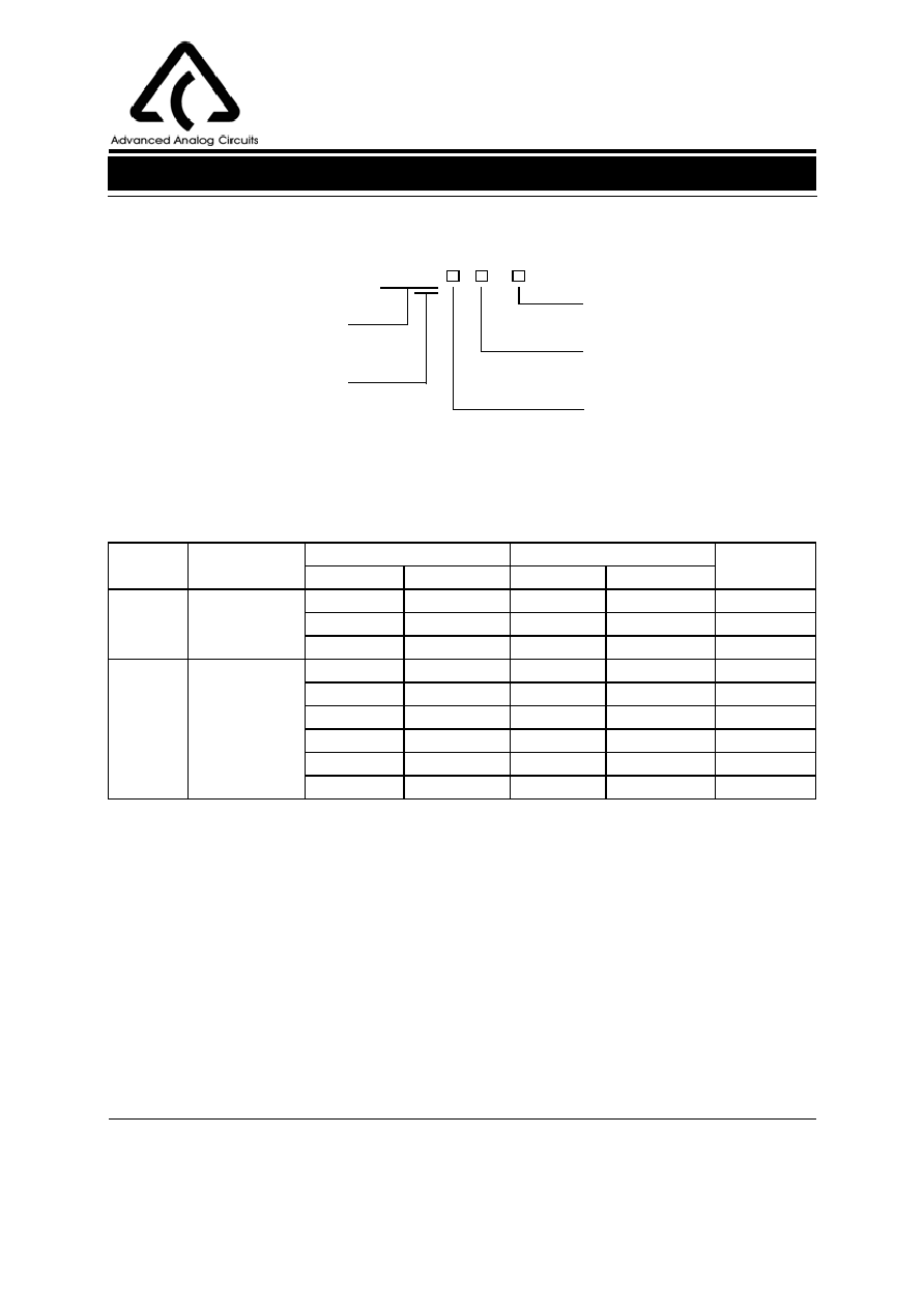
Ordering Information
Circuit Type
Package
AS78XX
T: TO-220-3
-
BCD Semiconductor's Pb-free products, as designated with "E1" suffix in the part number, are RoHS compliant.
E1: Lead Free
Output Voltage
05: 5V
D: TO-252-2
TR: Tape and Reel
Blank: Tube
12: 12V
15: 15V

3-TERMINAL 1A POSITIVE VOLTAGE REGULATOR AS78XX
Preliminary Datasheet
5
Mar. 2006 Rev. 1. 0
BCD Semiconductor Manufacturing Limited
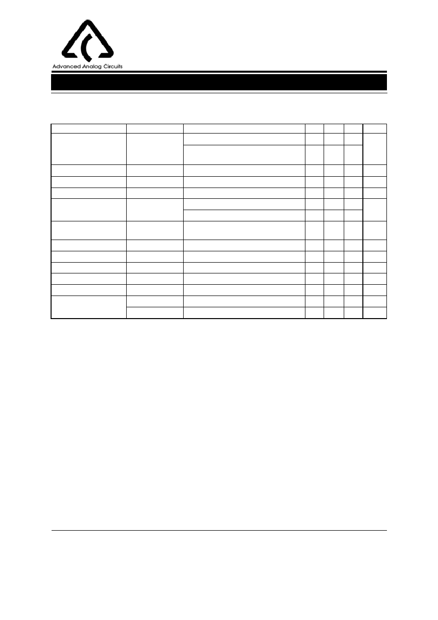
Recommended Operating Conditions
Parameter
Symbol
Min
Max
Unit
Operating Junction Temperature Range
T
J
-40
125
o
C
Absolute Maximum Ratings (Note 1)
Parameter Symbol
Value
Unit
Input Voltage
V
IN
35
V
Lead Temperature (Soldering, 10sec)
T
LEAD
260
o
C
Power Dissipation
P
D
Internally Limited
W
Storage Temperature Range
T
STG
-65 to 150
o
C
ESD (Machine Model)
ESD
400
V
Note 1: Stresses greater than those listed under "Absolute Maximum Ratings" may cause permanent damage to
the device. These are stress ratings only, and functional operation of the device at these or any other conditions
beyond those indicated under "Recommended Operating Conditions" is not implied. Exposure to "Absolute Max-
imum Ratings" for extended periods may affect device reliability.

3-TERMINAL 1A POSITIVE VOLTAGE REGULATOR AS78XX
Preliminary Datasheet
6
Mar. 2006 Rev. 1. 0
BCD Semiconductor Manufacturing Limited
Parameter
Symbol
Conditions
Min
Typ
Max
Unit
Output Voltage
V
OUT
T
J
=25
o
C
4.9
5
5.1
V
I
OUT
=5mA to 1A, V
IN
=7.5V to 20V,
P
D
15W
4.8
5.2
Line Regulation
V
RLINE
V
IN
=7.5 to 20V, I
OUT
=1A, T
J
=25
o
C
7
50
mV
Load Regulation
V
RLOAD
V
IN
=10V, I
OUT
=5mA to 1A, T
J
=25
o
C
25
100
mV
Quiescent Current
I
Q
V
IN
=10V
3.2
6
mA
Quiescent Current Change
I
Q
V
IN
=8 to 25V, I
OUT
=500mA, T
J
=25
o
C
0.3
0.8
mA
I
OUT
=5mA to 1A, T
J
=25
o
C
0.08
0.5
Ripple Rejection
PSRR
V
IN
=8 to 18V, f=120Hz, I
OUT
=500mA
73
dB
Dropout Voltage
V
DROP
V
OUT
=1%, I
OUT
=1A, T
J
=25
o
C
2
V
Output Noise Voltage
N
O
f=10Hz to 100kHz, T
A
=25
o
C
10
µV/V
O
Output Resistance
R
O
f=1kHz
10
m
Short Circuit Current
V
IN
=35V, T
A
=25
o
C
0.2
A
Peak Output Current
I
PK
V
IN
=10V, T
J
=25
o
C
2.2
A
Output Voltage
Temperature Coefficient
V
OUT
/
T
0.4
mV/
o
C
(V
OUT
/V
OUT
)/
T
80
ppm/
o
C
Electrical Characteristics
AS7805 (
V
IN
=10V, I
OUT
=1A, T
J
=-40 to 125
o
C, unless otherwise specified.
)
Parameter
Symbol
Conditions
Min
Typ
Max
Unit
Output Voltage
V
OUT
T
J
=25
o
C
11.75
12
12.25
V
I
OUT
=5mA to 1A, V
IN
=14.8V to 27V,
P
D
15W
11.5
12.5
Line Regulation
V
RLINE
V
IN
=14.8 to 27V, I
OUT
=1A, T
J
=25
o
C
16
120
mV
Load Regulation
V
RLOAD
V
IN
=19V, I
OUT
=5mA to 1A, T
J
=25
o
C
25
100
mV
Quiescent Current
I
Q
V
IN
=19V
3.4
6
mA
Quiescent Current Change
I
Q
V
IN
=15 to 30V, I
OUT
=500mA, T
J
=25
o
C
0.3
0.8
mA
I
OUT
=5mA to 1A, T
J
=25
o
C
0.08
0.5
Ripple Rejection
PSRR
V
IN
=15 to 25V, f=120Hz, I
OUT
=500mA
60
dB
Dropout Voltage
V
DROP
V
OUT
=1%, I
OUT
=1A, T
J
=25
o
C
2
V
Output Noise Voltage
N
O
f=10Hz to 100kHz, T
A
=25
o
C
10
µV/V
O
Output Resistance
R
O
f=1kHz
11
m
Short Circuit Current
V
IN
=35V, T
A
=25
o
C
0.2
A
Peak Output Current
I
PK
V
IN
=19V, T
J
=25
o
C
2.2
A
Output Voltage
Temperature Coefficient
V
OUT
/
T
0.96
mV/
o
C
(V
OUT
/V
OUT
)/
T
80
ppm/
o
C
AS7812 (
V
IN
=19V, I
OUT
=1A, T
J
=-40 to 125
o
C, unless otherwise specified.
)
3-TERMINAL 1A POSITIVE VOLTAGE REGULATOR AS78XX
Preliminary Datasheet
7
Mar. 2006 Rev. 1. 0
BCD Semiconductor Manufacturing Limited
Parameter
Symbol
Conditions
Min
Typ
Max
Unit
Output Voltage
V
OUT
T
J
=25
o
C
14.7
15
15.3
V
I
OUT
=5mA to 1A, V
IN
=17.9 to 30V,
P
D
15W
14.4
15.6
Line Regulation
V
RLINE
V
IN
=17.9 to 30V, I
OUT
=1A, T
J
=25
o
C
18
150
mV
Load Regulation
V
RLOAD
V
IN
=22V, I
OUT
=5mA to 1A, T
J
=25
o
C
25
100
mV
Quiescent Current
I
Q
V
IN
=23V
3.4
6
mA
Quiescent Current Change
I
Q
V
IN
=17.5 to 30V, I
OUT
=500mA, T
J
=25
o
C
0.3
0.8
mA
I
OUT
=5mA to 1A, T
J
=25
o
C
0.08
0.5
Ripple Rejection
PSRR
V
IN
=18.5 to 28.5V, f=120Hz,
I
OUT
=500mA
58
dB
Dropout Voltage
V
DROP
V
OUT
=1%, I
OUT
=1A, T
J
=25
o
C
2
V
Output Noise Voltage
N
O
f=10Hz to 100kHz, T
A
=25
o
C
10
µV/V
O
Output Resistance
R
O
f=1kHz
12
m
Short Circuit Current
V
IN
=35V, T
A
=25
o
C
0.2
A
Peak Output Current
I
PK
V
IN
=23V, T
J
=25
o
C
2.2
A
Output Voltage
Temperature Coefficient
V
OUT
/
T
1.2
mV/
o
C
(V
OUT
/V
OUT
)/
T
80
ppm/
o
C
Electrical Characteristics (Continued)
AS7815 (
V
IN
=23V, I
OUT
=1A, T
J
=-40 to 125
o
C, unless otherwise specified.
)

3-TERMINAL 1A POSITIVE VOLTAGE REGULATOR AS78XX
Preliminary Datasheet
8
Mar. 2006 Rev. 1. 0
BCD Semiconductor Manufacturing Limited
Typical Performance Characteristics
Figure 4. Peak Output Current vs. Input/Output
Differential Voltage
Figure 5. Output Voltage vs. Case Temperature
Figure 6. Quiescent Current vs. Case Temperature
Figure 7. Ripple Rejection vs. Frequency
3
6
9
12
15
18
21
24
0.0
0.5
1.0
1.5
2.0
2.5
Peak O
u
t
put Current
(A
)
V
IN
-V
OUT
(V)
AS7805
T
C
= -40
o
C
T
C
= 25
o
C
T
C
= 125
o
C
-40
-20
0
20
40
60
80
100
120
4.850
4.875
4.900
4.925
4.950
4.975
5.000
5.025
5.050
AS7805
V
IN
=10V
I
OUT
=10mA
O
u
t
put Voltage
(V
)
Case Temperature (
o
C)
-40
-20
0
20
40
60
80
100
120
0
1
2
3
4
5
6
Q
u
i
e
s
c
en
t
Cu
r
r
en
t
(mA
)
Case Temperature (
o
C)
I
OUT
=0
AS7805 V
IN
=10V
AS7812 V
IN
=19V
AS7815 V
IN
=23V
10
100
1k
10k
100k
1M
0
10
20
30
40
50
60
70
80
90
100
Rippl
e Re
ject
i
on (d
B
)
Frequency (Hz)
AS7805

3-TERMINAL 1A POSITIVE VOLTAGE REGULATOR AS78XX
Preliminary Datasheet
9
Mar. 2006 Rev. 1. 0
BCD Semiconductor Manufacturing Limited
Typical Performance Characteristics (Continued)
Figure 8. Dropout Voltage vs. Case Temperature
-40
-20
0
20
40
60
80
100
120
0.0
0.5
1.0
1.5
2.0
2.5
Dropo
ut
V
o
l
t
ag
e
(V)
Case Temperature (
o
C)
I
OUT
=100mA
I
OUT
=500mA
I
OUT
=1A
Figure 9. Power Dissipation vs. Case Temperature
V
OUT
(5
0m
V/
Div)
0
-50
Figure 11. Line Transient
V
IN
(
5
V/
Div)
Time (100
µ
s/Div)
(Conditions: I
OUT
=500mA, C
IN
=0.33
µ
F, C
OUT
=0.1
µ
F)
AS7805
10
15
-40
-20
0
20
40
60
80
100
120
0
5
10
15
20
25
30
P
o
wer Dis
s
ipa
t
ion
(
W
)
Case Temperature (
o
C)
AS7805
Package: TO-220-3
Heatsink Size: 45*43 mm
2
Figure 10. Power Dissipation vs. Case Temperature
-40
-20
0
20
40
60
80
100
120
0
5
10
15
20
25
30
P
o
w
e
r Diss
ipat
i
o
n
(
W
)
Case Temperature (
o
C)
AS7805
Package: TO-252-3
Heatsink Size: 45*43 mm
2

3-TERMINAL 1A POSITIVE VOLTAGE REGULATOR AS78XX
Preliminary Datasheet
10
Mar. 2006 Rev. 1. 0
BCD Semiconductor Manufacturing Limited
Typical Performance Characteristics (Continued)
I
OUT
(
1
A
/
D
i
v)
100
0
V
OUT
(1
00
mV
/
D
iv)
0
1
Figure 12. Load Transient
Time (40
µ
s/Div)
(Conditions: V
IN
=10V, C
IN
=0.33
µ
F, C
OUT
=0.1
µ
F)
AS7805
0.005A

3-TERMINAL 1A POSITIVE VOLTAGE REGULATOR AS78XX
Preliminary Datasheet
11
Mar. 2006 Rev. 1. 0
BCD Semiconductor Manufacturing Limited
Typical Application
Figure 13. Fixed Output Regulator of AS78XX
0.1
µ
F
0.33
µ
F
AS78XX
GND
INPUT
OUTPUT
V
IN
V
OUT

3-TERMINAL 1A POSITIVE VOLTAGE REGULATOR AS78XX
Preliminary Datasheet
12
Mar. 2006 Rev. 1. 0
BCD Semiconductor Manufacturing Limited
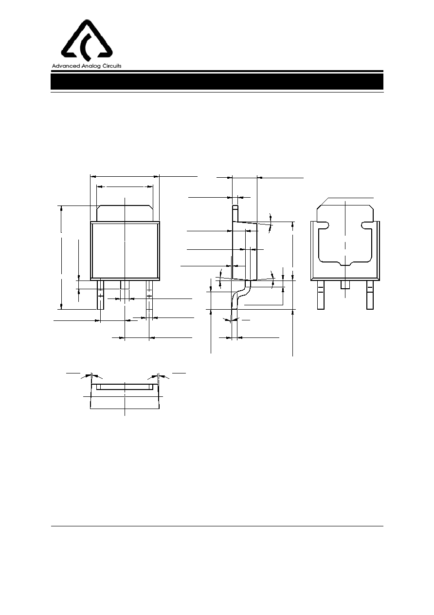
Mechanical Dimensions
TO-220-3
Unit: mm(inch)
3.560(0.140)
1
4
.
2
3
0
(
0
.
5
6
0
)
1.160(0.046)
0.813(0.032)
8.763(0.345)
2.540(0.100)
0.356(0.014)
2.080(0.082)
3
∞
7
∞
3.560(0.140)
7
∞
9.660(0.380)
0.550(0.022)
60
∞
0.381(0.015)
2.580(0.102)
60
∞
8
.
5
2
0
(
0
.
3
3
5
)
1.500(0.059)
0.200(0.008)
1
.
8
5
0
(
0
.
0
7
3
)
2.540(0.100)
0.381(0.015)
0.406(0.016)
3.380(0.133)
10.660(0.420)
4.060(0.160)
1.350(0.053)
2
7
.
8
8
0
(
1
.
0
9
8
)
3
0
.
2
8
0
(
1
.
1
9
2
)
9
.
5
2
0
(
0
.
3
7
5
)
1
6
.
5
1
0
(
0
.
6
5
0
)
4.820(0.190)
2.880(0.113)
1.760(0.069)
3-TERMINAL 1A POSITIVE VOLTAGE REGULATOR AS78XX
Preliminary Datasheet
13
Mar. 2006 Rev. 1. 0
BCD Semiconductor Manufacturing Limited
Mechanical Dimensions (Continued)
TO-252-2
Unit: mm(inch)
1
∞
7
∞
1
.
4
0
0
(
0
.
0
5
5
)
0.020(0.001)
0.460(0.018)
2.240(0.088)
0
.
6
5
0
(
0
.
0
2
6
)
9
.
5
0
0
(
0
.
3
7
4
)
0.750(0.030)
0.640(0.025)
5.230(0.206)
6.380(0.251)
2
.
6
0
0
(
0
.
1
0
2
)
5
.
3
6
0
(
0
.
2
1
1
)
2.180(0.086)
0.600(0.024)
5
∞
5
∞
8
∞
0.400(0.016)
0.510(0.020)
0.480(0.019)
1.080(0.043)
◊
45
∞
6.680(0.263)
0.580(0.023)
2.380(0.094)
5.430(0.214)
0
.
9
5
0
(
0
.
0
3
7
)
1
0
.
1
0
0
(
0
.
3
9
8
)
2.340(0.092)
2.240(0.088)
2.340(0.092)
0.780(0.031)
0.850(0.033)
1
.
7
6
0
(
0
.
0
6
9
)
5
.
5
6
0
(
0
.
2
1
9
)
1.320(0.052)
0.540(0.021)
0.120(0.005)
3
.
0
0
0
(
0
.
1
1
8
)
2.90
∞
3.10
∞
2.90
∞
3.10
∞

IMPORTANT NOTICE
BCD Semiconductor Manufacturing Limited reserves the right to make changes without further notice to any products or specifi-
cations herein. BCD Semiconductor Manufacturing Limited does not assume any responsibility for use of any its products for any
particular purpose, nor does BCD Semiconductor Manufacturing Limited assume any liability arising out of the application or use
of any its products or circuits. BCD Semiconductor Manufacturing Limited does not convey any license under its patent rights or
other rights nor the rights of others.
- Wafer Fab
Shanghai SIM-BCD Semiconductor Manufacturing Limited
800, Yi Shan Road, Shanghai 200233, China
Tel: +86-21-6485 1491, Fax: +86-21-5450 0008
BCD Semiconductor Manufacturing Limited
MAIN SITE
REGIONAL SALES OFFICE
Shenzhen Office
Shanghai SIM-BCD Semiconductor Manufacturing Co., Ltd. Shenzhen Office
Advanced Analog Circuits (Shanghai) Corporation Shenzhen Office
27B, Tower C, 2070, Middle Shen Nan Road, Shenzhen 518031, China
Tel: +86-755-8368 3987, Fax: +86-755-8368 3166
Taiwan Office
BCD Semiconductor (Taiwan) Company Limited
4F, 298-1, Rui Guang Road, Nei-Hu District, Taipei,
Taiwan
Tel: +886-2-2656 2808, Fax: +886-2-2656 2806
USA Office
BCD Semiconductor Corporation
3170 De La Cruz Blvd., Suite 105, Santa Clara,
CA 95054-2411, U.S.A
Tel: +1-408-988 6388, Fax: +1-408-988 6386
- IC Design Group
Advanced Analog Circuits (Shanghai) Corporation
8F, Zone B, 900, Yi Shan Road, Shanghai 200233, China
Tel: +86-21-6495 9539, Fax: +86-21-6485 9673
BCD Semiconductor Manufacturing Limited
http://www.bcdsemi.com