 | –≠–ª–µ–∫—Ç—Ä–æ–Ω–Ω—ã–π –∫–æ–º–ø–æ–Ω–µ–Ω—Ç: AZ317LZ | –°–∫–∞—á–∞—Ç—å:  PDF PDF  ZIP ZIP |
3-TERMINAL ADJUSTABLE REGULATOR AZ317L
Data Sheet
1
Apr. 2005 Rev. 1. 1
BCD Semiconductor Manufacturing Limited
General Description
The AZ317L is an adjustable 3-terminal positive volt-
age regulator capable of supplying 100mA over a 1.2V
to 12V output range. This voltage regulator is excep-
tionally easy to use and requires only two external
resistors to set the output voltage. Both line and load
regulation are better than standard fixed regulators.
In addition to higher performance than fixed regula-
tors, AZ317L employs overload protection. Included
on the chip are current limiting and thermal overload
protection. All overload protection circuitry remains
fully functional even when the adjustment terminal is
disconnected.
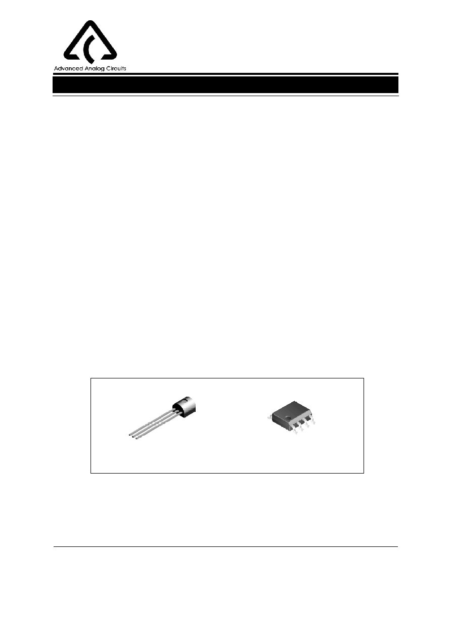
The AZ317L is available in standard TO-92 and SOIC-
8 packages.
Features
∑ Adjustable Output Down to 1.2V
∑ Guaranteed 100mA Output Current
∑ Output Short Circuit Protected
∑ Line Regulation: 0.01%/V
∑ Load Regulation: 0.1%
∑ Current Limit Constant with Temperature
∑ Standard 3-lead Transistor Package
∑ 70 dB Ripple Rejection
Applications
∑ High Efficiency Linear Regulators
∑ Post Regulation for Switching Supplies
∑ Microprocessor Power Supply
∑ Mother Board I/O Power Supply
Figure 1. Package Types of AZ317L
TO-92
SOIC-8

3-TERMINAL ADJUSTABLE REGULATOR AZ317L
Data Sheet
2
Apr. 2005 Rev. 1. 1
BCD Semiconductor Manufacturing Limited
Pin Configuration
Z Package
(TO-92)
Functional Block Diagram
Figure 3. Functional Block Diagram of AZ317L
8 NC
7 V
OUT
6 V
OUT
1
3
4
M Package
(SOIC-8)
5 NC
V
IN
V
OUT
V
OUT
ADJ
2
Figure 2. Pin Configuration of AZ317L
Top View
V
OUT
ADJ
V
IN
V
IN
V
OUT
ADJ
1
2
3
3-TERMINAL ADJUSTABLE REGULATOR AZ317L
Data Sheet
3
Apr. 2005 Rev. 1. 1
BCD Semiconductor Manufacturing Limited
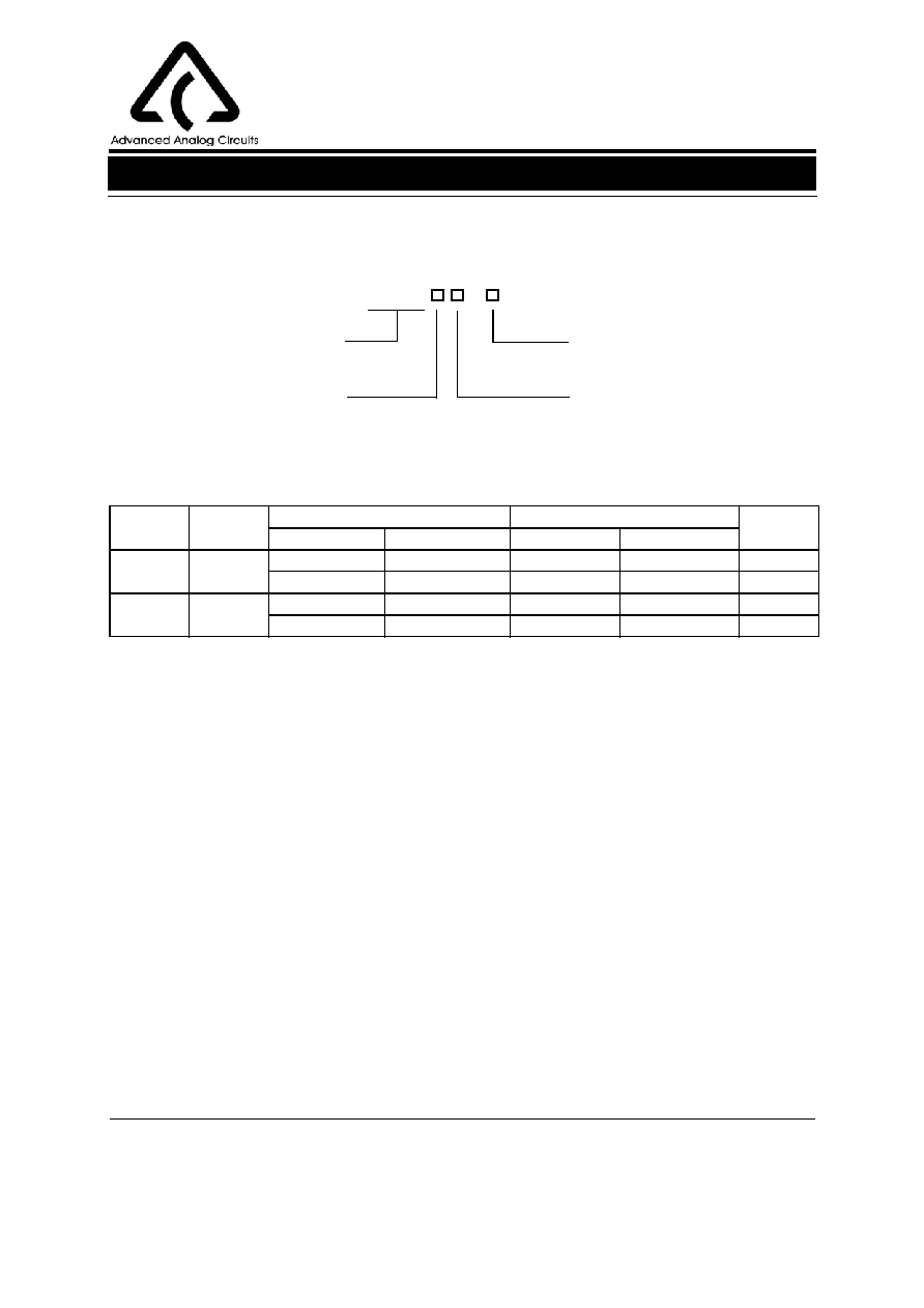
Package
Tempera-
ture Range
Part Number
Marking ID
Packing
Type
Tin Lead
Lead Free
Tin Lead
Lead Free
TO-92
0 to
125
o
C
AZ317LZ
AZ317LZ-E1
AZ317LZ
AZ317LZ-E1
Bulk
AZ317LZTR
AZ317LZTR-E1
AZ317LZ
AZ317LZ-E1
Ammo
SOIC-8
0 to
125
o
C
AZ317LM
AZ317LM-E1
317LM
317LM-E1
Tube
AZ317LMTR
AZ317LMTR-E1
317LM
317LM-E1
Tape & Reel
Circuit Type
Package
E1: Lead Free
Blank: Tin Lead
AZ317L -
TR: Tape and Reel or Ammo
Blank: Tube or Bulk
BCD Semiconductor's Pb-free products, as designated with "E1" suffix in the part number, are RoHS compliant.
Z: TO-92
M: SOIC-8
Ordering Information

3-TERMINAL ADJUSTABLE REGULATOR AZ317L
Data Sheet
4
Apr. 2005 Rev. 1. 1
BCD Semiconductor Manufacturing Limited
Recommended Operating Conditions
Parameter
Symbol
Value
Unit
Input Voltage
V
IN
20
V
Input-Output Voltage Differential
15
V
Operating Junction Temperature Range
T
J
150
o
C
Storage Temperature Range
T
STG
-65 to 150
o
C
Power Dissipation
P
D
700
mW
Lead Temperature (Soldering, 4 sec.)
T
LEAD
260
o
C
ESD (Machine Model)
ESD
250
V
Parameter
Symbol
Min
Max
Unit
Input Voltage
V
IN
15
V
Operating Junction Temperature Range
T
J
0
125
o
C
Note 1: Stresses greater than those listed under "Absolute Maximum Ratings" may cause permanent damage to the
device. These are stress ratings only, and functional operation of the device at these or any other conditions beyond
those indicated under "Recommended Operating Conditions" is not implied. Exposure to "Absolute Maximum
Ratings" for extended periods may affect device reliability.
Absolute Maximum Ratings (Note 1)

3-TERMINAL ADJUSTABLE REGULATOR AZ317L
Data Sheet
5
Apr. 2005 Rev. 1. 1
BCD Semiconductor Manufacturing Limited
Electrical Characteristics
0
o
C
T
J
125
o
C, V
IN
-V
OUT
= 5V, I
OUT
= 40mA, P
D
625mW, unless otherwise specified.
Parameter
Symbol
Conditions
Min
Typ
Max
Unit
Line Regulation
Reg
LINE
T
J
= 25
o
C, 3V
(V
IN
-V
OUT
)
15V
I
L
20mA (Note 2)
0.01
0.04
%/V
3V
(V
IN
-V
OUT
)
15V, I
L
20mA
(Note 2)
0.02
0.07
%/V
Load Regulation
Reg
LOAD
T
J
= 25
o
C, 5mA
I
OUT
100mA
(Note 2)
0.1
0.5
%
5mA
I
OUT
100mA (Note 2)
0.3
1.5
%
Thermal Regulation
T
J
= 25
o
C, 10ms Pulse
0.04
0.2
%/W
Adjust Pin Current
50
100
µA
Adjust Pin Current
Change
5mA
I
L
100mA
3V
(V
IN
-V
OUT
)
15V
0.2
5
µA
Reference Voltage
V
REF
3V
(V
IN
-V
OUT
)
15V
5mA
I
OUT
100mA
1.20
1.25
1.30
V
Current Limit
I
LIMIT
3V
(V
IN
-V
OUT
)
13V
100
200
300
mA
Minimum Load Cur-
rent
3V
(V
IN
-V
OUT
)
13V
3.5
5
mA
Ripple Rejection
V
OUT
= 10V, f = 120Hz, C
ADJ
= 0
µF
62
dB
V
OUT
= 10V, f = 120Hz, C
ADJ
= 10
µF 60
70
Temperature Stability
0
o
C
J
125
o
C
0.65
%
Long Term Stability
T
J
=125
o
C, 1000 Hours
0.3
1
%
RMS Output Noise,
% of V
OUT
T
J
= 25
o
C, 10Hz
f 10z
0.003
%
Thermal Resistance
Junction to Case
TO-92
SOIC-8
185
175
o
C/W
Note 2: Regulation is measured at constant junction temperature, using pulse testing with a low duty cycle.
Changes in output voltage due to heating effects are covered under the specification of thermal regulation.

3-TERMINAL ADJUSTABLE REGULATOR AZ317L
Data Sheet
6
Apr. 2005 Rev. 1. 1
BCD Semiconductor Manufacturing Limited
Typical Performance Characteristics
Figure 4. Load Regulation vs. Temperature
Figure 5. Output Voltage vs. Input Voltage
Figure 6. Reference Voltage vs. Temperature
Figure 7. Adjustment Current vs. Temperature
8
10
12
14
16
18
20
5.215
5.220
5.225
5.230
5.235
5.240
5.245
Out
put Voltage (V
)
Input Voltage (V)
AZ317L
I
O
=10mA
-25
0
25
50
75
100
125
-0.06
-0.04
-0.02
0.00
0.02
0.04
0.06
-45
I
O
=100mA
I
O
=10mA
O
u
tput Voltage Devi
at
i
on
(V)
Temperature (
o
C)
AZ317L
V
IN
=10.25V
V
OUT
=5.25V
-25
0
25
50
75
100
125
1.230
1.235
1.240
1.245
1.250
1.255
1.260
1.265
-45
I
O
=10mA
I
O
=100mA
R
e
f
e
re
nc
e V
o
l
t
a
g
e
(
V
)
Temperature(
O
C)
AZ317L
V
IN
=10.25V
V
OUT
=5.25V
-25
0
25
50
75
100
125
42
44
46
48
50
52
54
-45
I
O
=100mA
I
O
=10mA
Ad
j
u
s
t
P
i
n
C
u
r
r
ent
(
µ
A)
Temperature (
o
C)
AZ317L
V
IN
=10.25V
V
OUT
=5.25V

3-TERMINAL ADJUSTABLE REGULATOR AZ317L
Data Sheet
7
Apr. 2005 Rev. 1. 1
BCD Semiconductor Manufacturing Limited
Figure 8. Dropout Voltage vs. Temperature
Figure 9. Minimum Operating Current
Figure 10. Ripple Rejection vs. Output Voltage
Typical Performance Characteristics (Continued)
Figure 11. Ripple Rejection vs. Frequency
100
1000
10000
100000
0
10
20
30
40
50
60
70
80
C
ADJ
=0
µ
F
C
ADJ
=10
µ
F
R
i
p
p
le
R
e
je
c
t
io
n
(d
B
)
Frequency (Hz)
AZ317L
V
IN
=10.25V
V
OUT
=5.25V
I
O
=40mA
T
A
=25
o
C
2
4
6
8
10
12
14
16
0
10
20
30
40
50
60
70
80
C
ADJ
=0
µ
F
C
ADJ
=10
µ
F
R
i
ppl
e R
e
j
e
ct
i
on (
d
B
)
Output Voltage (V)
AZ317L
V
IN
-V
OUT
= 5V
I
O
= 40mA
f = 120Hz
T
A
= 25
o
C
-25
0
25
50
75
100
125
1.2
1.3
1.4
1.5
1.6
1.7
1.8
1.9
-45
I
O
=100mA
I
O
=10mA
Input O
u
t
p
ut Diff
erential (V
)
Temperature (
o
C)
AZ317L
V
OUT
=5.25V
2
4
6
8
10
12
14
16
0
1
2
3
4
5
6
Q
u
ie
s
c
ent Current
(m
A)
Input-Output Differential (V)
AZ317L
V
OUT
=5.25V
T
A
=25
o
C

3-TERMINAL ADJUSTABLE REGULATOR AZ317L
Data Sheet
8
Apr. 2005 Rev. 1. 1
BCD Semiconductor Manufacturing Limited
Typical Performance Characteristics (Continued)
Figure 12. Load Transient Response
Figure 13. Line Transient Response
AZ317L
I
O
=40mA
V
OUT
=5.25V
C
IN
=0.1
µ
F
C
L
=1
µ
F
T
A
=25
o
C
V
OUT
V
IN
(10.25V to 11.25V)
L
oad
Ou
tpu
t
V
o
ltag
e
D
e
vi
at
i
o
n
C
u
rr
ent
Inp
u
t V
o
lt
age
C
han
ge
O
u
tp
ut V
o
l
t
age
De
via
t
io
n
O
u
tp
ut V
o
lta
g
e
D
e
viat
i
o
n
D
i
s
s
i
pa
t
i
on
V
OUT
AZ317L
V
OUT
=5.25V
C
IN
=0.1
µ
F
C
L
=1
µ
F
T
A
=25
o
C
Power=1W
1W
Figure 14. Thermal Regulation
50mA
AZ317L
V
IN
=10.25V
V
OUT
=5.25V
C
IN
=0.1
µ
F
C
L
=1
µ
F
T
A
=25
o
C
V
OUT
I
OUT
(5mA to 100mA)

3-TERMINAL ADJUSTABLE REGULATOR AZ317L
Data Sheet
9
Apr. 2005 Rev. 1. 1
BCD Semiconductor Manufacturing Limited
Figure 16. Current Limited 6V Charger
Figure 17. High Stability 10V Regulator
Figure 15. 5V Logic Regulator with Electronic
Note 3: Sets peak current, I
Peak
= 0.6V/R4
Figure 18. Adjustable Regulator with
Improved Ripple Rejection
Shutdown (Minimum output = 1.2V)
Note 4: 1000
µ
F is recommended to filter out
Note 5: Discharge C1 if output is shorted
any input transients.
to ground.
R2
720
V
IN
V
OUT
ADJ
C1
0.1
µ
F
R1
240
C2
0.1
µ
F
1K
Q1
2N2219
AZ317L
5V
V
IN
TTL
7V ~
18V
V
OUT
R3
R2
5K
V
IN
V
OUT
ADJ
C2
0.1
µ
F
R1
240
C3
1
µ
F
Solid
Tantalum
AZ317L
V
IN
C1
10
µ
F
D1
1N4002
V
OUT
R4 10
(Note 3)
V
IN
V
OUT
ADJ
C1
1000
µ
F
(Note 4)
R1
240
R3 100
Q1
2N2222
AZ317L
V
IN
9V ~
18V
R2
1.1K
R3
267
1%
V
IN
V
OUT
ADJ
C1
0.1
µ
F
R1
2K
5%
AZ317L
10V
V
IN
15V
V
OUT
R2
1.5K
1%
D1
LM329
Typical Application

3-TERMINAL ADJUSTABLE REGULATOR AZ317L
Data Sheet
10
Apr. 2005 Rev. 1. 1
BCD Semiconductor Manufacturing Limited
Figure 19. Adjustable Regulator with Current Limit
Note 6: Short circuit current is approximately
600mV/R3 or 60mA
Note 7: At 2.5mA output only 3/4V of drop occurs
in R3 and R4.
Figure 20. Slow Turn-on 15V Regulator
V
IN
V
OUT
ADJ
AZ317L
V
IN
V
OUT
1N4002
R1
240
15V
2N2905
R1
2.7k
C2
0.1
µ
F
R3
50k
C1
25
µ
F
R4=2R3=22
V
IN
V
OUT
ADJ
R1
120
R3 10
Q1
2N2219
AZ317L
Transformer
Rectifiers
and Filter
Capacitor
V
OUT
= 1.25V(R2/R1 +1)
+
-
R2
2K
Typical Application (Continued)

3-TERMINAL ADJUSTABLE REGULATOR AZ317L
Data Sheet
11
Apr. 2005 Rev. 1. 1
BCD Semiconductor Manufacturing Limited
Mechanical Dimensions
Unit: mm(inch)
2.440(0.096)
2.640(0.104)
0.380(0.015)
0.550(0.022)
1.600(0.063)
MAX
14
.1
00
(
0
.
5
55
)
14
.5
00
(
0
.
5
71
)
1.270(0.050)
TYP
3.
3
0
0
(
0.
1
3
0
)
3.
7
0
0
(
0.
1
4
6
)
4.30
0(
0.
16
9)
4.70
0(
0.
18
5)
1.100(0.043)
1.400(0.055)
4.400(0.173)
4.700(0.185)
3.430(0.135)
MIN
0.360(0.014)
0.510(0.020)
0.000(0.000)
0.380(0.015)
TO-92

3-TERMINAL ADJUSTABLE REGULATOR AZ317L
Data Sheet
12
Apr. 2005 Rev. 1. 1
BCD Semiconductor Manufacturing Limited
Mechanical Dimensions (Continued)
Unit: mm(inch)
0
∞
8
∞
1
∞
5
∞
R0.150(0.006)
R0
.15
0
(0
.00
6
)
1.000(0.039)
0.330(0.013)
0.510(0.020)
4.800(0.189)
5.000(0.197)
1.350(0.053)
1.750(0.069)
0.100(0.004)
0.300(0.012)
0.900(0.035)
0.800(0.031)
0.200(0.008)
3.800(0.150)
4.000(0.157)
7
∞
7
∞
20:1
D
1.270(0.050)
TYP
0.190(0.007)
0.250(0.010)
8
∞
D
5.800(0.228)
6.200(0.244)
0.675(0.027)
0.725(0.029)
0.320(0.013)
8
∞
SOIC-8

8F, B Zone, 900 Yi Shan Road, Shanghai 200233, PRC Tel: +86-21-6495 9539, Fax: +86-21-6485 9673
BCD Semiconductor (Taiwan) Company Limited
4F, 298-1 Rui Guang Road, Nei-Hu District, Taipei, Taiwan Tel: +886-2-2656-2808, Fax: +886-2-2656-2806
IMPORTANT NOTICE
BCD Semiconductor Manufacturing Limited reserves the right to make changes without further notice to any pro-
ducts or specifications herein. BCD Semiconductor Manufacturing Limited does not assume any responsibility for
use of any its products for any particular purpose, nor does BCD Semiconductor Manufacturing Limited assume any
liability arising out of the application or use of any its products or circuits. BCD Semiconductor Manufacturing Limi-
ted does not convey any license under its patent rights or other rights nor the rights of others.
http://www.bcdsemi.com
BCD Semiconductor Corporation
3170 De La Cruz Blvd, Suite # 105 Santa Clara, CA 95054-2411, U.S.A Tel: +1-408-988 6388, Fax: +1-408-988 6386
Shanghai SIM-BCD Semiconductor Manufacturing Co., Ltd.
800 Yi Shan Road, Shanghai 200233, PRC Tel: +86-21-6485 1491, Fax: +86-21-5450 0008
Advanced Analog Circuits (Shanghai) Corporation