 | –≠–ª–µ–∫—Ç—Ä–æ–Ω–Ω—ã–π –∫–æ–º–ø–æ–Ω–µ–Ω—Ç: AZ358 | –°–∫–∞—á–∞—Ç—å:  PDF PDF  ZIP ZIP |

LOW POWER DUAL OPERATIONAL AMPLIFIERS AZ358
1
Issue Date: Jan. 2003
Advanced Analog Circuits
Data Sheet
Rev. 1.0
General Description
The AZ358 consists of two independent, high gain and
internally frequency compensated operational amplifi-
ers, it is specifically designed to operate from a single
power supply. Operation from split power supply is
also possible and the low power supply current drain is
independent of the magnitude of the power supply
voltages.
Features
∑
Internally frequency compensation
∑
Large voltage gain
∑
Low input bias current
∑
Low input offset voltage
∑
Large output voltage swing
∑
Wide power supply voltage range:
Single supply 3V to 18V
or dual supplies
±
1.5V to
±
9V
∑
Low supply current drain: 500uA
∑
Compatible with industry standard 358
Applications
∑
Battery Charger
∑
Cordless Telephone
∑
Switching Power Supply
DIP-8
SOIC-8
Figure 1. Package Types of AZ358
(SOIC-8/DIP-8)
Pin Configuration
OUTPUT 1
INPUT 1+
INPUT 1-
GND
8 V
cc
7 OUTPUT 2
6 INPUT 2-
5 INPUT 2+
1
2
3
4
Top View
Figure 2. Pin Configuration of AZ358
M Package/P Package

LOW POWER DUAL OPERATIONAL AMPLIFIERS AZ358
2
Issue Date: Jan. 2003
Advanced Analog Circuits
Data Sheet
Rev. 1.0
Ordering Information
Package
Temperature Range
Part Number
Packing Type
SOIC-8
-40
o
C~85
o
C
AZ358M
Tube/Reel
DIP-8
AZ358P
Tube
Figure 3. Functional Block Diagram of AZ358
(Each Amplifier)
Functional Block Diagram
Q2
Q4
Q3
Q1
Q8
Q9
6uA
4uA
Q10
Q11
50uA
Q5
Q6
Q13
Rsc
Cc
100uA
Q7
INPUTS
+
-
OUTPUT
Q12

LOW POWER DUAL OPERATIONAL AMPLIFIERS AZ358
3
Issue Date: Jan. 2003
Advanced Analog Circuits
Data Sheet
Rev. 1.0
Parameter
Symbol Value
Unit
Power Supply Voltage
V
CC
20
V
Differential Input Voltage
V
ID
20
V
Input Voltage
V
IC
-0.3 to 20
V
Input Current (V
IN
<-0.3V) (Note 2)
I
IN
50
mA
Output Short-Circuit to Ground
(One Amplifier) (Note 3)
V
CC
12V an T
A
= 25
o
C
Continuous
Power Dissipation
P
D
DIP-8
830
mW
SOIC-8
550
Operating Temperature Range
T
OP
-40 to 85
o
C
Storage Temperature Range
T
STG
-65 to 150
o
C
Lead Temperature (Soldering, 10 Seconds)
260
o
C
ESD (Machine Mode)
200
V
Note 1: Stresses greater than those listed under "Absolute Maximum Ratings" may cause permanent damage to
the device. These are stress ratings only, and functional operation of the device at these or any other conditions
beyond those indicated under "Recommended Operation Ratings" is not implied. Exposure to "Absolute Maxi-
mum Ratings" for extended periods may affect device reliability.
Note 2: This input current will only exist when the voltage at any of the input leads is driven negative. It is due to
the collector-base junction of the input PNP transistors becoming forward biased and thereby acting as input
diode clamps. In addition to this diode action, there is also lateral NPN parasitic transistor action on the IC chip.
This transistor action can cause the output voltages of the op amps to go to the V
CC
voltage level (or to ground for
a large overdrive) for the time duration that an input is driven negative. This is not destructive and normal output
states will re-establish when the input voltage, which was negative, again returns to a value greater than -0.3V (at
25
o
C)
Note 3: Short circuits from the output to V
CC
can cause excessive heating and eventual destruction. When consid-
ering short circuits to ground, the maximum output current is approximately 40mA independent of the magnitude
of V
CC
. At values of supply voltage in excess of +12V, continuous short-circuits can exceed the power dissipation
ratings and cause eventual destruction. Destructive dissipation can result from simultaneous shorts on all amplifi-
ers.
Absolute Maximum Ratings (Note 1)
(Operation temperature range applies unless otherwise specified.)

LOW POWER DUAL OPERATIONAL AMPLIFIERS AZ358
4
Issue Date: Jan. 2003
Advanced Analog Circuits
Data Sheet
Rev. 1.0
Electrical Characteristics
Parameter
Symbol
Test Conditions
Min. Typ.
Max.
Unit
Input Offset Voltage
V
IO
Vo:1.4V,R
S
: 0
,V
CC
: 5V to 15V
2
5
mV
Input Bias Current
(Note 4)
I
BIAS
I
IN
+ or I
IN
-, V
CM
=0V
20
200
nA
Input Offset Current
I
IO
I
IN
+ or I
IN
-, V
CM
=0V
5
50
nA
Input Common Mode
Voltage Range (Note 5)
V
IR
V
CC
=15V
0
V
CC
-1.5 V
Supply Current
I
CC
R
L
=
, Over full
t e m p e r a t u r e
range on all OP
Amps
V
CC
=15V
0.7
1.5
mA
V
CC
=5V
0.5
1.2
Large Signal Voltage Gain
G
V
V
CC
=15V, R
L
2, V
0
=1V to
11V
80
90
dB
Common Mode Rejection Ratio
CMRR
V
CM
=0V to (V
CC
-1.5)V
70
90
dB
Power Supply Rejection Ration
PSRR
V
CC
=5V to 15V
70
90
dB
Channel Separation
(Note 6)
CS
f=1KHz to 20KHz
-120
dB
Output Current
Source
I
SOURCE
V+=1V,V-=0V,
V
CC
=15V,V
0
=2V
20
45
mA
Sink
I
SINK
V+=0V,V-=1V,
V
CC
=15V, V
0
=2V
10
20
mA
V+=0V,V-=1V,
V
CC
=15V,V
0
=200mV
12
50
uA
Short Circuit to Ground
I
SC
V
CC
=15V
45
60
mA
Output Voltage Swing
V
OH
V
CC
=15V, R
L
=2K
12
V
V
CC
=15V, R
L
=10K
12.5
13.5
V
OL
V
CC
=5V, R
L
=10K
5
20
mV
Note 4: The direction of the input current is out of the IC due to the PNP input stage. This current is essentially
constant, independent of the state of the output so no loading change exists on the input lines.
Note 5: The input common-mode voltage of either input signal voltage should not be allowed to go negatively by
more than 0.3V (at 25
o
C). The upper end of the common-mode voltage range is V
CC
- 1.5V (at 25
o
C), but either
or both inputs can go to +18V without damages, independent of the magnitude of the V
CC
.
Note 6: Due to proximity of external components, insure that coupling is not originating via stray capacitors
between these external parts. This typically can be detected as this type of capacitance increases at higher fre-
quencies.
Vcc=5V, GND=0, T
A
=25
o
C unless otherwise specified.
LOW POWER DUAL OPERATIONAL AMPLIFIERS AZ358
5
Issue Date: Jan. 2003
Advanced Analog Circuits
Data Sheet
Rev. 1.0
V
CC
- POWER SUPPLY VOLTAGE (V
DC
)
I
D
-
S
U
P
P
L
Y
CUR
REN
T
D
R
AIN (m
A
DC
)
A
VOL
-
V
O
L
T
AG
E GA
IN (
d
B
)
V
CC
- POWER SUPPLY VOLTAGE (V)
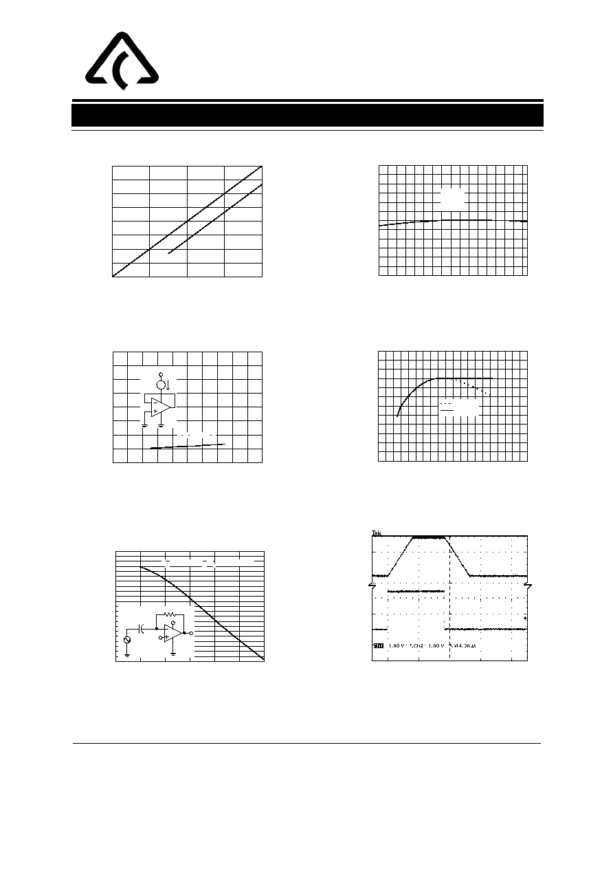
Figure 4. Input Voltage Range
Figure 6. Supply Current
Figure 7. Voltage Gain
Figure 8. Open Loop Frequency Response
Figure 9. Voltage Follower Pulse Response
Figure 5. Input Current
0
2
4
6
8
10
12
14
16
18
20
0.0
0.5
1.0
1.5
2.0
2.5
3.0
3.5
4.0
T
A
:0
o
C TO 85
o
C
0
2
4
6
8
0
1
2
3
4
5
6
7
8
POSITIVE
NEGATIVE
-40
-20
0
20
40
60
80
100
120
0
5
10
15
20
25
30
V
CC
=15V
1HZ
10HZ
100HZ
1kHZ
10kHZ
100kHZ
1MHZ
0
10
20
30
40
50
60
70
80
90
100
110
V
CC
: 10V TO 15V
DC
T
A
: -40
o
C TO 85
o
C
R 10M
V
IN
V
CC
/2
V
O
V
CC
0.1uF
A
I
D
mA
V
CC
Typical Characteristics
0
2
4
6
8
10
12
14
16
18
20
60
70
80
90
100
110
120
R
L
=2K
R
L
=20K
V
CC
- POWER SUPPLY VOLTAGE (±V
DC
)
±V
IN
-
IN
PU
T VO
L
T
AGE
(
±
V
DC
)
I
B -
INP
U
T CURRE
NT (n
A
DC
)
T
A
- TEMPERATURE (
o
C)
V
IN
- IN
PU
T
t - TIME (uS)
V
OU
T
-
OUTP
U
T
VOL
T
AGE
(V
)
V
OL
T
A
G
E
(
V
)
0
3
1
2
0
1
3
2
0
10
20
30
40
50
f - FREQUENCY (Hz)
A
VOL
-
VOL
T
AGE
GAIN
(d
B)
V
CC
=15V
R
L
= 2K