
1.5A ULTRA LOW DROPOUT LINEAR REGULATOR AZ39150
Preliminary Datasheet
1
Apr. 2005 Rev. 1. 1
BCD Semiconductor Manufacturing Limited
General Description
The AZ39150 is low dropout three-terminal regulator
with a typical dropout of 375mV at 1.5A output cur-
rent.
The AZ39150 provides current limit and thermal shut-
down. On-chip thermal shutdown provides protection
against any combination of high current and ambient
temperature that would create excessive junction tem-
peratures.
The AZ39150 is available for 3.3V and 5.0V versions
now. It is available in the industry standard TO-220-3
and TO-263-3 power packages.
Features
∑
Minimum Guaranteed Output Current: 1.5A
∑
Dropout Voltage: 375mV at I
OUT
=1.5A
∑
Output Accuracy: 1%
∑
Low Ground Current
∑
Internal Current Limit and Thermal Protection
∑
Reversed-battery and Reversed-lead Insertion
Protection
∑
Fast Transient Response
Applications
∑
LCD TV
∑
Set Top Box
∑
LCD Monitor
∑
SMPS Post Regulator
∑
Laptop, Palmtop and Notebook
∑
Portable Instrumentation
∑
USB Power Supply
Figure 1. Package Types of AZ39150
TO-220-3
TO-263-3

1.5A ULTRA LOW DROPOUT LINEAR REGULATOR AZ39150
Preliminary Datasheet
2
Apr. 2005 Rev. 1. 1
BCD Semiconductor Manufacturing Limited
Pin Number
Pin Name
Function
1
V
IN
Unregulated input.
2
GND
The ground pin. This pin and TAB are internally connected.
3
V
OUT
Regulated Output.
Pin Configuration
Figure 2. Pin Configuration of AZ39150 (Top View)
3
2
1
3
2
1
V
OUT
GND
V
IN
V
OUT
GND
V
IN
T Package
(TO-220-3)
S Package
(TO-263-3)
Pin Description

1.5A ULTRA LOW DROPOUT LINEAR REGULATOR AZ39150
Preliminary Datasheet
3
Apr. 2005 Rev. 1. 1
BCD Semiconductor Manufacturing Limited
Functional Block Diagram
Figure 3. Functional Block Diagram of AZ39150
16V
Thermal
Shutdown
Reference
+
-
1.24V
V
IN
V
OUT
GND
1
2
3
AZ39150
-
Package
Circuit Type
T: TO-220-3
S: TO-263-3
Blank: Tin Lead
E1: Lead Free
TR: Tape and Reel
3.3: Fixed Output 3.3V
Blank: Tube
5.0: Fixed Output 5.0V
Ordering Information

1.5A ULTRA LOW DROPOUT LINEAR REGULATOR AZ39150
Preliminary Datasheet
4
Apr. 2005 Rev. 1. 1
BCD Semiconductor Manufacturing Limited
Package
Temperature
Range
Part Number
Marking ID
Packing
Type
Tin Lead
Lead Free
Tin Lead
Lead Free
AZ39150T-3.3
AZ39150T-3.3E1
AZ39150T-3.3
AZ39150T-3.3E1
Tube
AZ39150T-5.0
AZ39150T-5.0E1
AZ39150T-5.0
AZ39150T-5.0E1
Tube
TO-263-3
AZ39150S-3.3
AZ39150S-3.3E1
AZ39150S-3.3
AZ39150S-3.3E1
Tube
AZ39150S-3.3TR AZ39150S-3.3TRE1 AZ39150S-3.3
AZ39150S-3.3E1 Tape & Reel
AZ39150S-5.0
AZ39150S-5.0E1
AZ39150S-5.0
AZ39150S-5.0E1
Tube
AZ39150S-5.0TR AZ39150S-5.0TRE1 AZ39150S-5.0
AZ39150S-5.0E1 Tape & Reel
BCD Semiconductor's Pb-free products, as designated with "E1" suffix in the part number, are RoHS compliant.
Note 1:
Stresses greater than those listed under "Absolute Maximum Ratings" may cause permanent damage to
the device. These are stress ratings only, and functional operation of the device at these or any other conditions
beyond those indicated under "Recommended Operating Conditions" is not implied. Exposure to "Absolute Max-
imum Ratings" for extended periods may affect device reliability.
Parameter Symbol
Value
Unit
Supply Voltage
V
IN
15
V
Maximum Operating Junction Temperature
T
J
150
o
C
Storage Temperature Range
T
STG
-65 to 150
o
C
Lead Temperature (Soldering, 10sec)
T
LEAD
300
o
C
ESD (Machine Model)
300
V
Absolute Maximum Ratings (Note 1)
Recommended Operating Conditions
Parameter
Symbol
Min
Max
Unit
Supply Voltage
V
IN
13.2
V
Operating Junction Temperature
T
J
-40
125
o
C
TO-220-3
-40 to 125
o
C
-40 to 125
o
C
Ordering Information (Continued)

1.5A ULTRA LOW DROPOUT LINEAR REGULATOR AZ39150
Preliminary Datasheet
5
Apr. 2005 Rev. 1. 1
BCD Semiconductor Manufacturing Limited
Parameter
Symbol
Condition
Min
Typ
Max
Unit
Output Voltage
V
OUT
I
OUT
=10mA
3.27
3.3
3.33
V
10mA
I
OUT
1.5A, 4.3VV
IN
8V
3.23
3.3
3.37
V
Line Regulation
V
RLINE
I
OUT
=10mA, 4.3V
V
IN
8V
2
17
mV
Load Regulation
V
RLOAD
V
IN
=4.3V, 10mA
I
OUT
1.5A
6.6
33
mV
Output Voltage
Temperature Coefficient
V
OUT
/
T
I
OUT
=10mA
66
330
µV/
o
C
Dropout Voltage (Note 2)
V
OUT
=1% I
OUT
=100mA
80
200
mV
I
OUT
=750mA
260
mV
I
OUT
=1.5A
375
500
mV
Ground Current
I
GND
I
OUT
=750mA, V
IN
=4.3V
4
20
mA
I
OUT
=1.5A, V
IN
=4.3V
17
mA
Current Limit
I
LIMIT
V
OUT
=0V (Note 3)
2.0
2.8
A
Minimum Load Current
I
LOAD
(MIN)
7
10
mA
Output Noise Voltage (rms)
10Hz to 100KHz, I
OUT
=100mA,
C
OUT
=10
µF
400
µV
Electrical Characteristics
V
DROP
Note 2: Dropout voltage is defined as the input-to-output differential when the output voltage drops to 99% of its norminal
value which is measured at V
OUT
+1V applied to V
IN
.
Note 3: V
IN
=V
OUT(NOMINAL)
+1V.
Operating Conditions: V
IN
=4.3V, I
OUT
=10mA, C
IN=
10
µF, C
OUT
=10
µF,
T
J
=25
o
C, unless otherwise specified. The
Boldface applies over -40
o
C
T
J
125
o
C.
AZ39150-3.3V Electrical Characteristics

1.5A ULTRA LOW DROPOUT LINEAR REGULATOR AZ39150
Preliminary Datasheet
6
Apr. 2005 Rev. 1. 1
BCD Semiconductor Manufacturing Limited
Electrical Characteristics (Continued)
Parameter
Symbol
Condition
Min
Typ
Max
Unit
Output Voltage
V
OUT
I
OUT
=10mA
4.95
5.0
5.05
V
10mA
I
OUT
1.5A, 6VV
IN
8V
4.90
5.0
5.10
V
Line Regulation
V
RLINE
I
OUT
=10mA, 6V
V
IN
8V
3
25
mV
Load Regulation
V
RLOAD
V
IN
=6V, 10mA
I
OUT
1.5A
10
50
mV
Output Voltage
Temperature Coefficient
V
OUT
/
T
I
OUT
=10mA
100
500
µV/
o
C
Dropout Voltage (Note 2)
V
OUT
=1% I
OUT
=100mA
80
200
mV
I
OUT
=750mA
260
mV
I
OUT
=1.5A
375
500
mV
Ground Current
I
GND
I
OUT
=750mA, V
IN
=6V
4
20
mA
I
OUT
=1.5A, V
IN
=6V
17
mA
Current Limit
I
LIMIT
V
OUT
=0V (Note 3)
2.0
2.8
A
Minimum Load Current
I
LOAD
(MIN)
7
10
mA
Output Noise Voltage (rms)
10Hz to 100KHz, I
OUT
=100mA,
C
OUT
=10
µF
400
µV
V
DROP
Operating Conditions: V
IN
=6V, I
OUT
=10mA, C
IN=
10
µF, C
OUT
=10
µF,
T
J
=25
o
C, unless otherwise specified. The
Boldface applies over -40
o
C
T
J
125
o
C.
AZ39150-5.0V Electrical Characteristics
Note 2: Dropout voltage is defined as the input-to-output differential when the output voltage drops to 99% of its norminal
value which is measured at V
OUT
+1V applied to V
IN
.
Note 3: V
IN
=V
OUT(NOMINAL)
+1V.

1.5A ULTRA LOW DROPOUT LINEAR REGULATOR AZ39150
Preliminary Datasheet
7
Apr. 2005 Rev. 1. 1
BCD Semiconductor Manufacturing Limited
Typical Performance Characteristics
Figure 4. Dropout Voltage vs. Output Current
Figure 5. Dropout Voltage vs. Temperature
Figure 6. Ground Current vs. Output Current
Figure 7. Ground Current vs. Supply Voltage
0
250
500
750
1000
1250
1500
0
50
100
150
200
250
300
350
400
450
500
Dropout Voltage
(m
V)
Output Current (mA)
V
OUT
=5.0V
-25
0
25
50
75
100
125
0
50
100
150
200
250
300
350
400
450
500
550
600
Dropout Voltage (mV)
Temperature (
o
C)
I
OUT
=1.5A
V
OUT
=5.0V
0
250
500
750
1000
1250
1500
0.0
2.5
5.0
7.5
10.0
12.5
15.0
17.5
20.0
22.5
25.0
G
r
ound
Current (m
A)
Output Current (mA)
V
IN
=6V
V
OUT
=5.0V
0
2
4
6
8
10
12
0.0
0.1
0.2
0.3
0.4
0.5
0.6
0.7
0.8
0.9
1.0
1.1
1.2
1.3
1.4
1.5
1.6
1.7
1.8
G
r
ound
Current (mA
)
Supply Voltage (V)
V
OUT
=5.0V
I
OUT
=10mA
I
OUT
=100mA

1.5A ULTRA LOW DROPOUT LINEAR REGULATOR AZ39150
Preliminary Datasheet
8
Apr. 2005 Rev. 1. 1
BCD Semiconductor Manufacturing Limited
Typical Performance Characteristics (Continued)
Figure 9. Ground Current vs. Temperature
Figure 10. Ground Current vs. Temperature
Figure 11. Ground Current vs. Temperature
Figure 8. Ground Current vs. Supply Voltage
0
2
4
6
8
10
12
0
5
10
15
20
25
30
35
40
45
50
G
r
ound Current
(m
A)
Supply Voltage (V)
V
OUT
=5.0V
I
OUT
=750mA
I
OUT
=1000mA
I
OUT
=1500mA
-25
0
25
50
75
100
125
0.27
0.28
0.29
0.30
0.31
0.32
0.33
0.34
0.35
0.36
0.37
G
r
ound Current
(m
A)
Temperature (
o
C)
V
IN
=6V
V
OUT
=5.0V
I
OUT
=10mA
-25
0
25
50
75
100
125
0
1
2
3
4
5
6
7
8
G
r
ound Current
(m
A)
Temperature (
o
C)
V
IN
=6V
V
OUT
=5.0V
I
OUT
=750mA
-25
0
25
50
75
100
125
10
11
12
13
14
15
16
17
18
19
20
G
r
ou
nd Cu
r
r
en
t
(
m
A)
Temperature (
o
C)
V
IN
=6V
V
OUT
=5.0V
I
OUT
=1.5A

1.5A ULTRA LOW DROPOUT LINEAR REGULATOR AZ39150
Preliminary Datasheet
9
Apr. 2005 Rev. 1. 1
BCD Semiconductor Manufacturing Limited
Typical Performance Characteristics (Continued)
Figure 13. Load Transient
Figure 14. Load Transient
Figure 15. Line Transient
Figure 12. Output Voltage vs. Temperature
-25
0
25
50
75
100
125
4.95
4.96
4.97
4.98
4.99
5.00
5.01
5.02
5.03
5.04
5.05
O
u
t
p
ut
V
o
l
t
ag
e
(V)
Temperature (
o
C)
V
IN
=6V
V
OUT
=5.0V
I
OUT
=10mA
Out
put C
u
rrent
Outpu
t
V
o
lta
ge
I
npu
t V
o
l
t
a
g
e
O
utp
u
t V
o
lta
ge
Outp
ut C
u
rrent
Out
p
ut
V
o
lt
age
C
L
=10
µ
F
C
L
=47
µ
F
I
OUT
=10mA
V
OUT
=5.0V
V
OUT
=5.0V
V
OUT
=5.0V

1.5A ULTRA LOW DROPOUT LINEAR REGULATOR AZ39150
Preliminary Datasheet
10
Apr. 2005 Rev. 1. 1
BCD Semiconductor Manufacturing Limited
Figure 16. Typical Application of AZ39150
V
IN
V
OUT
GND
+
V
IN
V
OUT
AZ39150
10µF
10
µF
1
3
2
+
Typical Application

1.5A ULTRA LOW DROPOUT LINEAR REGULATOR AZ39150
Preliminary Datasheet
11
Apr. 2005 Rev. 1. 1
BCD Semiconductor Manufacturing Limited
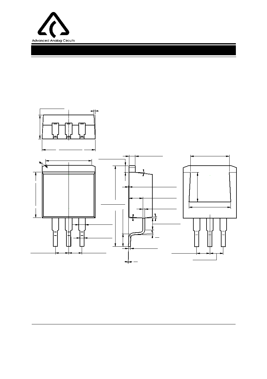
Mechanical Dimensions
TO-220-3
Unit: mm(inch)
3.560(0.140)
1
4
.
2
3
0
(
0
.
5
6
0
)
1.160(0.046)
0.813(0.032)
8.763(0.345)
2.540(0.100)
0.356(0.014)
2.080(0.082)
3
∞
7
∞
3.560(0.140)
7
∞
9.660(0.380)
0.550(0.022)
60
∞
0.381(0.015)
2.580(0.102)
60
∞
8
.
5
2
0
(
0
.
3
3
5
)
1.500(0.059)
0.200(0.008)
1
.
8
5
0
(
0
.
0
7
3
)
2.540(0.100)
0.381(0.015)
0.406(0.016)
3.380(0.133)
10.660(0.420)
4.060(0.160)
1.350(0.053)
2
7
.
8
8
0
(
1
.
0
9
8
)
3
0
.
2
8
0
(
1
.
1
9
2
)
9
.
5
2
0
(
0
.
3
7
5
)
1
6
.
5
1
0
(
0
.
6
5
0
)
4.820(0.190)
2.880(0.113)
1.760(0.069)
1.5A ULTRA LOW DROPOUT LINEAR REGULATOR AZ39150
Preliminary Datasheet
12
Apr. 2005 Rev. 1. 1
BCD Semiconductor Manufacturing Limited
Mechanical Dimensions (Continued)
TO-263-3
Unit: mm(inch)
7
∞
3
∞
7
∞
8
.
6
4
0
(
0
.
3
4
0
)
9
.
6
5
0
(
0
.
3
8
0
)
0.990(0.039)
0.510(0.020)
2.540(0.100)
1.150(0.045)
9.650(0.380)
3
∞
14.760(0.581)
8.840(0.348)
2.640(0.104)
0.020(0.001)
8
∞
2
∞
0
∞
6
∞
0.380(0.015)
2
.
3
9
0
(
0
.
0
9
4
)
0.360(0.014)
2.200(0.087)
70
∞
10.290(0.405)
4.070(0.160)
4.820(0.190)
1.390(0.055)
1.150(0.045)
1.390(0.055)
2.540(0.100)
1.270(0.050)
1.390(0.055)
2
.
6
9
0
(
0
.
1
0
6
)
15.740(0.620)
0.250(0.010)
2.700(0.106)
0.400(0.016)
5
.
6
0
0
(
0
.
2
2
0
)
7.420(0.292)
7.980(0.314)
2.540(0.100)
2.540(0.100)

http://www.bcdsemi.com
8F, B Zone, 900 Yi Shan Road, Shanghai 200233, PRC Tel: +86-21-6495 9539, Fax: +86-21-6485 9673
BCD Semiconductor (Taiwan) Company Limited
Room 2210, 22nd Fl, 333, Keelung Road, Sec. 1, TaiPei (110), Taiwan Tel: +886-2-2758 6828, Fax: +886-2-2758 6892
IMPORTANT NOTICE
BCD Semiconductor Manufacturing Limited reserves the right to make changes without further notice to any pro-
ducts or specifications herein. BCD Semiconductor Manufacturing Limited does not assume any responsibility for
use of any its products for any particular purpose, nor does BCD Semiconductor Manufacturing Limited assume any
liability arising out of the application or use of any its products or circuits. BCD Semiconductor Manufacturing Limi-
ted does not convey any license under its patent rights or other rights nor the rights of others.
BCD Semiconductor Corporation
3170 De La Cruz Blvd, Suite # 105 Santa Clara, CA 95054-2411, U.S.A Tel: +1-408-988 6388, Fax: +1-408-988 6386
Shanghai SIM-BCD Semiconductor Manufacturing Co., Ltd.
800 Yi Shan Road, Shanghai 200233, PRC Tel: +86-21-6485-1491, Fax: +86-21-5450-0008
Advanced Analog Circuits (Shanghai) Corporation