
VOLTAGE DETECTOR AZ70XX
AZ70XX
Preliminary Datasheet
1
Jul. 2005 Rev. 1. 3
BCD Semiconductor Manufacturing Limited
General Description
The AZ70XX series ICs are under voltage detectors
with a built in voltage threshold and low power con-
sumption. The AZ70XX are specifically designed to
accurately monitor power supplies.
The AZ70XX use a precision on-chip voltage refer-
ence and a comparator to measure the input operating
voltage. These ICs can accurately reset the system after
detecting voltage at the time of switching power on and
instantaneous power off in various CPU systems and
other logic systems. The detect voltage thresholds are
2.3V/2.5V/2.7V/2.9V/3.1V/3.3V/4.2V/4.5Vfor
AZ7023/25/27/29/31/33/42/45 respectively. Built in
hysteresis helps to prevent erratic operation in the pres-
ence of noise.
The AZ70XX series are available in 2 standard pack-
ages: TO-92 and SOT-89-3.
Features
∑
Low Current Consumption:
I
CCL
=300
µA
Typical
I
CCH
=30
µA
Typical
∑
Low Minimum Operating Voltage for Output
Resetting: 0.8V Typical
∑
Built in Hysteresis Voltage: 50mV Typical
∑
Open Collector Output
∑
Extended Temperature Range: -40 to 85
o
C
Applications
∑
Low Battery Voltage Detector
∑
Power Fail Indicator
∑
Processor Reset Generator
∑
Battery Backup Control
∑
Home Electric Appliances
TO-92
SOT-89-3
Figure 1. Package Types of AZ70XX
VOLTAGE DETECTOR AZ70XX
AZ70XX
Preliminary Datasheet
2
Jul. 2005 Rev. 1. 3
BCD Semiconductor Manufacturing Limited
Figure 2. Pin Configuration of AZ70XX (Top View)
Z Package
(TO-92)
R Package
(SOT-89-3)
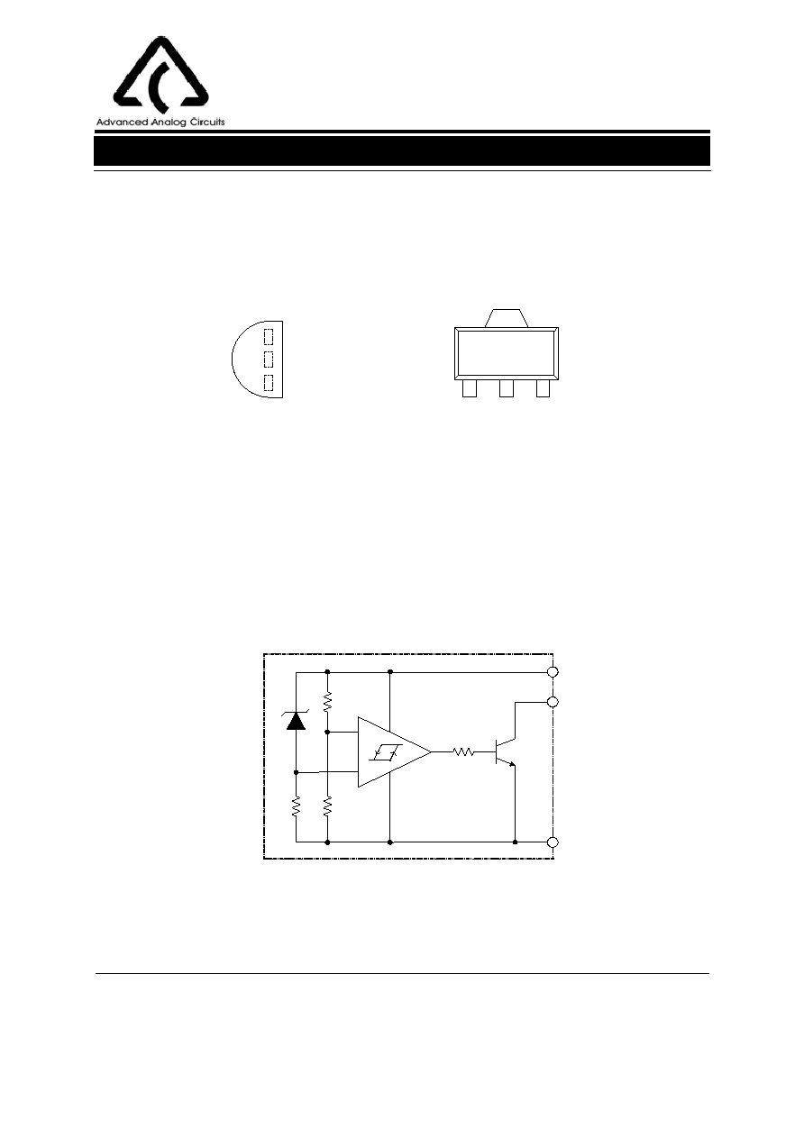
Figure 3. Functional Block Diagram of AZ70XX
Functional Block Diagram
V
CC
GND OUT
1
2
3
OUT
GND
V
CC
+
-
V
CC
OUT
GND
1
2
3
Pin Configuration

VOLTAGE DETECTOR AZ70XX
AZ70XX
Preliminary Datasheet
3
Jul. 2005 Rev. 1. 3
BCD Semiconductor Manufacturing Limited
Ordering Information
Package
Temperature
Range
Detector
Voltage
Part Number
Marking ID
Packing Type
Tin Lead
Lead Free
Tin Lead
Lead Free
TO-92
-40 to 85
o
C
2.3V
AZ7023Z
AZ7023Z-E1
AZ7023Z
AZ7023Z-E1
Bulk
AZ7023ZTR
AZ7023ZTR-E1
AZ7023Z
AZ7023Z-E1
Ammo
2.5V
AZ7025Z
AZ7025Z-E1
AZ7025Z
AZ7025Z-E1
Bulk
AZ7025ZTR
AZ7025ZTR-E1
AZ7025Z
AZ7025Z-E1
Ammo
2.7V
AZ7027Z
AZ7027Z-E1
AZ7027Z
AZ7027Z-E1
Bulk
AZ7027ZTR
AZ7027ZTR-E1
AZ7027Z
AZ7027Z-E1
Ammo
2.9V
AZ7029Z
AZ7029Z-E1
AZ7029Z
AZ7029Z-E1
Bulk
AZ7029ZTR
AZ7029ZTR-E1
AZ7029Z
AZ7029Z-E1
Ammo
3.1V
AZ7031Z
AZ7031Z-E1
AZ7031Z
AZ7031Z-E1
Bulk
AZ7031ZTR
AZ7031ZTR-E1
AZ7031Z
AZ7031Z-E1
Ammo
3.3V
AZ7033Z
AZ7033Z-E1
AZ7033Z
AZ7033Z-E1
Bulk
AZ7033ZTR
AZ7033ZTR-E1
AZ7033Z
AZ7033Z-E1
Ammo
4.2V
AZ7042Z
AZ7042Z-E1
AZ7042Z
AZ7042Z-E1
Bulk
AZ7042ZTR
AZ7042ZTR-E1
AZ7042Z
AZ7042Z-E1
Ammo
4.5V
AZ7045Z
AZ7045Z-E1
AZ7045Z
AZ7045Z-E1
Bulk
AZ7045ZTR
AZ7045ZTR-E1
AZ7045Z
AZ7045Z-E1
Ammo
SOT-89-3
-40 to 85
o
C
2.3V
AZ7023RTR
AZ7023RTR-E1
7023R
E723
Tape & Reel
2.5V
AZ7025RTR
AZ7025RTR-E1
7025R
E725
Tape & Reel
2.7V
AZ7027RTR
AZ7027RTR-E1
7027R
E727
Tape & Reel
2.9V
AZ7029RTR
AZ7029RTR-E1
7029R
E729
Tape & Reel
3.1V
AZ7031RTR
AZ7031RTR-E1
7031R
E731
Tape & Reel
3.3V
AZ7033RTR
AZ7033RTR-E1
7033R
E733
Tape & Reel
4.2V
AZ7042RTR
AZ7042RTR-E1
7042R
E742
Tape & Reel
4.5V
AZ7045RTR
AZ7045RTR-E1
7045R
E745
Tape & Reel
Circuit Type
Package
Z: TO-92
E1: Lead Free
Blank: Tin Lead
AZ70
-
TR: Tape and Reel or Ammo
Blank: Bulk
R: SOT-89-3
Detect Voltage
23: 2.3V
27: 2.7V
29: 2.9V
33: 3.3V
42: 4.2V
45: 4.5V
25: 2.5V
BCD Semiconductor's Pb-free products, as designated with "E1" suffix in the part number, are RoHS compliant.
31: 3.1V

AZ70XX
Preliminary Datasheet
4
Jul. 2005 Rev. 1. 3
BCD Semiconductor Manufacturing Limited
VOLTAGE DETECTOR AZ70XX
Note 1:
Stresses greater than those listed under "Absolute Maximum Ratings" may cause permanent damage to
the device. These are stress ratings only, and functional operation of the device at these or any other conditions
beyond those indicated under"Recommended Operating Conditions" is not implied. Exposure to "Absolute Maxi-
mum Ratings" for extended periods may affect device reliability.
Recommended Operating Conditions
Parameter Symbol
Min
Max
Unit
Supply Voltage
V
CC
-0.3
18
V
Power Dissipation (Package Limitations)
P
D
TO-92 Package: 500
mW
SOT-89-3 Package: 400
Storage Temperature Range
T
STG
-65
150
o
C
ESD (Machine Model)
ESD
500
V
ESD (Human Body Mode)
ESD
5000
V
Parameter
Symbol
Min
Max
Unit
Supply Voltage
V
CC
15
V
Operating Temperature Range
T
OPR
-40
85
o
C
Absolute Maximum Ratings (Note 1)

AZ70XX
Preliminary Datasheet
5
Jul. 2005 Rev. 1. 3
BCD Semiconductor Manufacturing Limited
VOLTAGE DETECTOR AZ70XX
Electrical Characteristics
Operating Conditions: T
A
=25
o
C unless otherwise specified.
Parameter
Symbol
Conditions
Min
Typ
Max
Unit
Detecting Voltage
V
S
R
L
=200
(Note 2)
V
OL
0.4V
AZ7023R/Z
2.15
2.3
2.45
V
AZ7025R/Z
2.35
2.5
2.65
AZ7027R/Z
2.55
2.7
2.85
AZ7029R/Z
2.75
2.9
3.05
AZ7031R/Z
2.95
3.1
3.25
AZ7033R/Z
3.15
3.3
3.45
AZ7042R/Z
4.05
4.2
4.35
AZ7045R/Z
4.35
4.5
4.65
Low-Level Output Voltage
V
OL
V
CC
=V
S
(min)-0.05V
R
L
=200
(Note 2)
0.4
V
Output Leakage Current
I
OH
V
CC
=15V
0.1
µA
Hysteresis Voltage
V
HYS
R
L
=200
(Note 2)
30
50
100
mV
Detect Voltage Temperature
Coefficient
V
S
/(V
S
◊
T) R
L
=200
(Note 2)
±0.01
% /
o
C
Circuit Current at On Time
I
CCL
V
CC
=V
S
(min)-0.05V
300
500
µA
Circuit Current at Off Time
I
CCH
V
CC
=5.25V
30
50
µA
Minimum Operating Voltage
V
OPR
R
L
=200
(Note 2)
V
OL
0.4V
0.8
V
"
L" Transmission Delay Time
tpHL
V
CC
changed from 5.25V to
V
S
(min)-0.05V, R
L
=1.0K
,
C
L
=100p (Note 3)
10
µs
"
H" Transmission Delay Time
tpLH
V
CC
changed from V
S
(min)-
0.05V to 5.25V, R
L
=1.0K
,
C
L
=100p (Note 3)
15
µs
Output Current at On Time
I
OL
V
CC
=V
S
(min)-0.05V
T
A
=25
o
C (Note 4)
20
mA
I
OL
V
CC
=V
S
(min)-0.05V
T
A
=-40 to 85
o
C (Note 4)
16
Note 2: See test circuit 1 and Figure 12.
Note 3: See test circuit 2 and Figure 12.
Note 4: See test circuit 3. Adjusting the regulative power source until the reading value of voltage meter V is 0.4V,
the reading value of current meter A is defined as "Output Current at On Time".

VOLTAGE DETECTOR AZ70XX
AZ70XX
Preliminary Datasheet
6
Jul. 2005 Rev. 1. 3
BCD Semiconductor Manufacturing Limited
Figure 4. Test Circuit 1
Figure 5. Test Circuit 2
Electrical Characteristics (Continued)
Figure 5. Test Circuit 2
Figure 6. Test Circuit 3
10
µ
F
+
A
V
V
S
(min)-0.05V
1
3
2
V
CC
AZ7029
OUT
GND
R
L
10
µ
F
+
A2
V2
A1
V1
1
3
2
V
CC
AZ7029
OUT
GND
C
L
+5V
R
L
10
µ
F
+
Input
Pulse
1
3
2
V
CC
AZ7029
OUT
GND

AZ70XX
Preliminary Datasheet
7
Jul. 2005 Rev. 1. 3
BCD Semiconductor Manufacturing Limited
VOLTAGE DETECTOR AZ70XX
Figure 7. Detecting Voltage vs. Temperature
Figure 8. Minimum Operating Voltage vs. Temperature
Figure 9. Output Current at on Time vs. Temperature
Figure 10. Low-level Output Voltage vs. Temperature
-40
-20
0
20
40
60
80
400
500
600
700
800
900
1000
1100
1200
AZ7029
M
i
nim
u
m
Opera
t
ing Volt
ag
e (mV
)
Temperature (
O
C)
-40
-20
0
20
40
60
80
10
20
30
40
50
60
70
Ou
tp
ut
C
u
r
r
e
n
t
a
t
on
t
i
m
e
(
m
A)
Temperature (
O
C)
AZ7029
-40
-20
0
20
40
60
80
0
25
50
75
100
AZ7029
Low-lev
el
O
u
t
put
Vo
lta
ge (mV
)
Temperature (
O
C)
-40
-20
0
20
40
60
80
2.75
2.80
2.85
2.90
2.95
V
S
-V
HYS
(V
CC
Falling)
V
S
(V
CC
Rising)
Detect
ing V
o
lt
age (
V
)
Temperature (
O
C)
AZ7029
Typical Performance Characteristics

VOLTAGE DETECTOR AZ70XX
AZ70XX
Preliminary Datasheet
8
Jul. 2005 Rev. 1. 3
BCD Semiconductor Manufacturing Limited
Figure 11. Output Voltage Dynamic Response when V
CC
Increases and Decreases
Time (s)
Figure 12. AZ70XX Timing Waveform
Operating Diagram
V
CC
V
OUT
tpLH
tpLH
tpHL
V
S
V
S
-V
HYS
Typical Performance Characteristics (Continued)

AZ70XX
Preliminary Datasheet
9
Jul. 2005 Rev. 1. 3
BCD Semiconductor Manufacturing Limited
VOLTAGE DETECTOR AZ70XX
Figure 13. Low Voltage Indicator
Figure 14. CPU Resetting Circuit
1
3
2
V
CC
AZ70XX
OUT
GND
LED
V
CC
R1
220
V
CC
+5V
R1
3.3k
1
3
2
V
CC
AZ70XX
OUT
GND
CPU
V
CC
GND
RESET
C1
1
µ
F
+
Figure 12 is a typical timing waveform for AZ70XX
during power-up and temporary power-down period.
Here is some explanations for AZ70XX's operation.
1. During power-up period, V
OUT
will remain
undefined until V
CC
rises above V
OPR
(typically
0.8V). After that moment, the output will become
valid and will be at its logic low state while
V
OPR
<V
CC
<V
S
for power-up operating.
2. After a delay time of tpLH from the moment
V
CC
>V
S
, the V
OUT
will be at its logic high state. In
general, V
OUT
is dependent upon the voltage that the
pull up resistor connected to.
3. During power-down, after a delay time of tpHL
from the moment V
CC
<V
S
-V
HYS
, V
OUT
will be at its
logic low state. In general, at rated output current and
V
CC,
V
OUT
can be pulled down to a voltage as low as
within 0.4V from GND. (See the Electrical
Characteristics section).
4. V
OUT
will be at its logic low state while V
S
-
V
HYS
>V
CC
>V
OPR
for power-down operating.
5. After V
CC
falls below V
OPR
, the output is
undefined.
Operating Diagram (Continued)
Typical Applications

VOLTAGE DETECTOR AZ70XX
AZ70XX
Preliminary Datasheet
10
Jul. 2005 Rev. 1. 3
BCD Semiconductor Manufacturing Limited
TO-92
Mechanical Dimensions
Unit: mm
(
inch
)
2.440(0.096)
2.640(0.104)
0.380(0.015)
0.550(0.022)
1.600(0.063)
MAX
1
4
.1
00
(0.5
55
)
1
4
.5
00
(0.5
71
)
1.270(0.050)
TYP
3
.
3
0
0
(
0
.
130)
3
.
7
0
0
(
0
.
146)
4.
30
0(
0
.
1
6
9
)
4.
70
0(
0
.
1
8
5
)
1.100(0.043)
1.400(0.055)
4.400(0.173)
4.700(0.185)
3.430(0.135)
MIN
0.360(0.014)
0.510(0.020)
0.000(0.000)
0.380(0.015)

AZ70XX
Preliminary Datasheet
11
Jul. 2005 Rev. 1. 3
BCD Semiconductor Manufacturing Limited
VOLTAGE DETECTOR AZ70XX
Mechanical Dimensions (Continued)
SOT-89-3
Unit: mm(inch)
1.400(0.055)*
1.630(0.064)
4.400(0.173)
0.360(0.014)
0.440(0.017)
3.000(0.118)
0
.
9
0
0
(
0
.
0
3
5
)
2.300(0.091)
3
.
9
5
0
(
0
.
1
5
6
)
1.400(0.055)
0.360(0.014)
10
∞
3
∞
10
∞
R0.200(0.008)
R0.150(0.006)
0.000(0.000)
3
∞
1.600(0.063)
0.440(0.017)
0.560(0.022)
2.600(0.102)
0.480(0.019)
4.600(0.181)
1.830(0.072)
1
.
2
0
0
(
0
.
0
4
7
)
4
.
2
5
0
(
0
.
1
6
7
)
0.076(0.003)
0.360(0.014)
0.480(0.019)

8F, B Zone, 900 Yi Shan Road, Shanghai 200233, PRC Tel: +86-21-6495 9539, Fax: +86-21-6485 9673
BCD Semiconductor (Taiwan) Company Limited
4F, 298-1 Rui Guang Road, Nei-Hu District, Taipei, Taiwan Tel: +886-2-2656-2808, Fax: +886-2-2656-2806
IMPORTANT NOTICE
BCD Semiconductor Manufacturing Limited reserves the right to make changes without further notice to any pro-
ducts or specifications herein. BCD Semiconductor Manufacturing Limited does not assume any responsibility for
use of any its products for any particular purpose, nor does BCD Semiconductor Manufacturing Limited assume any
liability arising out of the application or use of any its products or circuits. BCD Semiconductor Manufacturing Limi-
ted does not convey any license under its patent rights or other rights nor the rights of others.
http://www.bcdsemi.com
BCD Semiconductor Corporation
3170 De La Cruz Blvd, Suite # 105 Santa Clara, CA 95054-2411, U.S.A Tel: +1-408-988 6388, Fax: +1-408-988 6386
Shanghai SIM-BCD Semiconductor Manufacturing Co., Ltd.
800 Yi Shan Road, Shanghai 200233, PRC Tel: +86-21-6485 1491, Fax: +86-21-5450 0008
Advanced Analog Circuits (Shanghai) Corporation