Continental Device India Limited
Data Sheet
Page 1 of 3
TIP100, 101, 102
NPN PLASTIC POWER TRANSISTORS
TIP105, 106, 107
PNP PLASTIC POWER TRANSISTORS
Power Darlingtons for Linear and Switching Applications
ABSOLUTE MAXIMUM RATINGS
100 101 102
105 106 107
Collector-base voltage (open emitter)
V
CBO
max. 60
80
100
V
Collector-emitter voltage (open base)
V
CEO
max. 60
80
100
V
Collector current
I
C
max.
8.0
A
Total power dissipation up to T
C
= 25∞C
P
tot
max.
80
W
Junction temperature
T
j
max.
150
∞C
Collector-emitter saturation voltage
I
C
= 3 A; I
B
= 6 mA
V
CEsat
max.
2.0
V
D.C. current gain
I
C
= 3 A; V
CE
= 4 V
h
FE
min.
1.0
K
max.
20
K
RATINGS (at T
A
=25∞C unless otherwise specified)
Limiting values
100 101 102
105 106 107
Collector-base voltage (open emitter)
V
CBO
max. 60
80
100
V
Collector-emitter voltage (open base)
V
CEO
max. 60
80
100
V
Emitter-base voltage (open collector)
V
EBO
max.
5.0
V
TIP100, TIP101, TIP102
TIP105, TIP106, TIP107
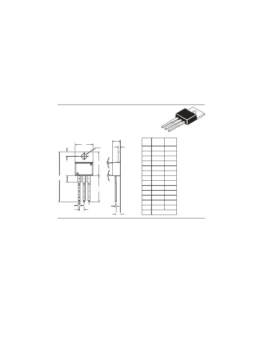
PIN CONFIGURATION
1. BASE
2. COLLECTOR
3. EMITTER
4. COLLECTOR
B
1 2
3
J
M
G
D
H
A
O
O
K
N
L
F
E
C
D IM
M IN .
M A X.
A
l
l
di
m
i
ns
i
ons
i
n
m
m
.
A
14.42
16.51
B
9.63
10.67
C
3.56
4.83
D
0.90
E
1.15
1.40
F
3.75
3.88
G
2.29
2.79
H
2.54
3.43
J
0.56
K
12.70
14.73
L
2.80
4.07
M
2.03
2.92
N
31.24
O
D E G 7
1
2
3
4
IS / IECQC 700000
IS / IECQC 750100
IS/ISO 9002
Lic# QSC/L- 000019.2
Continental Device India Limited
An IS/ISO 9002 and IECQ Certified Manufacturer
TO-220 Plastic Package
Boca Semicondcutor Corp.
BSC
http://www.bocasemi.com page: 1

Continental Device India Limited
Data Sheet
Page 2 of 3
Collector current
I
C
max.
8.0
A
Collector peak current
I
CM
max.
15
A
Base current
I
B
max.
1.0
A
Total power dissipation up to T
C
= 25∞C P
tot
max.
80
W
Derate above 25∞C
max
0.64
W/∞ C
Total power dissipation up to T
A
= 25∞C P
tot
max.
2.0
W
Derate above 25∞C
max
0.016
W/∞ C
Junction temperature
T
j
max.
150
∞C
Storage temperature
T
stg
≠65 to +150
∞C
THERMAL RESISTANCE
From junction to ambient
R
th j≠a
62.5
∞C/W
From junction to case
R
th j≠c
1.56
∞C/W
CHARACTERISTICS
T
amb
= 25∞C unless otherwise specified
100 101 102
105 106 107
Collector cutoff current
I
B
= 0; V
CE
= 30 V
I
CEO
max. 50
≠
≠
µA
I
B
= 0; V
CE
= 40 V
I
CEO
max.
≠
50
≠
µA
I
B
= 0; V
CE
= 50 V
I
CEO
max.
≠
≠
50
µA
I
E
= 0; V
CB
= 60V
I
CBO
max. 50
≠
≠
µA
I
E
= 0; V
CB
= 80V
I
CBO
max.
≠
50
≠
µA
I
E
= 0; V
CB
= 100V
I
CBO
max.
≠
≠
50
µA
Emitter cut-off current
I
C
= 0; V
EB
= 5 V
I
EBO
max.
8
mA
Breakdown voltages
I
C
= 30 mA; I
B
= 0
V
CEO(sus)
*
min.
60
80
100 V
I
C
= 1 mA; I
E
= 0
V
CBO
min.
60
80
100 V
I
E
= 1 mA; I
C
= 0
V
EBO
min.
5.0
V
Saturation voltages
I
C
= 3 A; I
B
= 6 mA
V
CEsat
*
max.
2.0
V
I
C
= 8 A; I
B
= 80 mA
V
CEsat
*
max.
2.5
V
Base-emitter on voltage
I
C
= 8 A; V
CE
= 4 V
V
BE(on)
*
max.
2.8
V
D.C. current gain
I
C
= 3 A; V
CE
= 4 V
h
FE
*
min.
1.0
K
max.
20
K
I
C
= 8 A; V
CE
= 4 V
h
FE
*
min.
200
Small signal current gain
I
C
= 3A; V
CE
= 4V; f = 1.0 MHz
|h
fe
|
min.
4.0
Output capacitance f = 0.1 MHz
I
E
= 0; V
CB
= 10V,
PNP
C
o
max.
300
pF
NPN
max.
200
pF
Forward voltage of commutation diode
I
F
= ≠I
C
= 10A; I
B
= 0
V
F
*
max.
2.8
V
* Pulsed: pulse duration = 300 µs; duty cycle
2%.
TIP100, TIP101, TIP102
TIP105, TIP106, TIP107
http://www.bocasemi.com page: 2