Continental Device India Limited
Data Sheet
Page 1 of 3
TIP 41, 41A, 41B, 41C
NPN PLASTIC POWER TRANSISTORS
TIP 42, 42A, 42B, 42C
PNP PLASTIC POWER TRANSISTORS
General Purpose Amplifier and Switching Applications
ABSOLUTE MAXIMUM RATINGS
41 41A 41B 41C
42 42A 42B 42C
Collector-base voltage (open emitter)
V
CBO
max. 40
60
80
100
V
Collector-emitter voltage (open base)
V
CEO
max. 40
60
80
100
V
Collector current
I
C
max.
6.0
A
Total power dissipation up to T
C
= 25∞C P
tot
max.
65
W
Junction temperature
T
j
max.
150
∞C
Collector-emitter saturation voltage
I
C
= 6 A; I
B
= 0.6 A
V
CEsat
max.
1.5
V
D.C. current gain
I
C
= 3 A; V
CE
= 4 V
h
FE
min.
15
max.
75
RATINGS (at T
A
=25∞C unless otherwise specified)
41 41A 41B 41C
Limiting values
42 42A 42B 42C
Collector-base voltage (open emitter)
V
CBO
max. 40
60
80
100
V
Collector-emitter voltage (open base)
V
CEO
max. 40
60
80
100
V
Emitter-base voltage (open collector)
V
EBO
max.
5.0
V
Collector current
I
C
max.
6.0
A
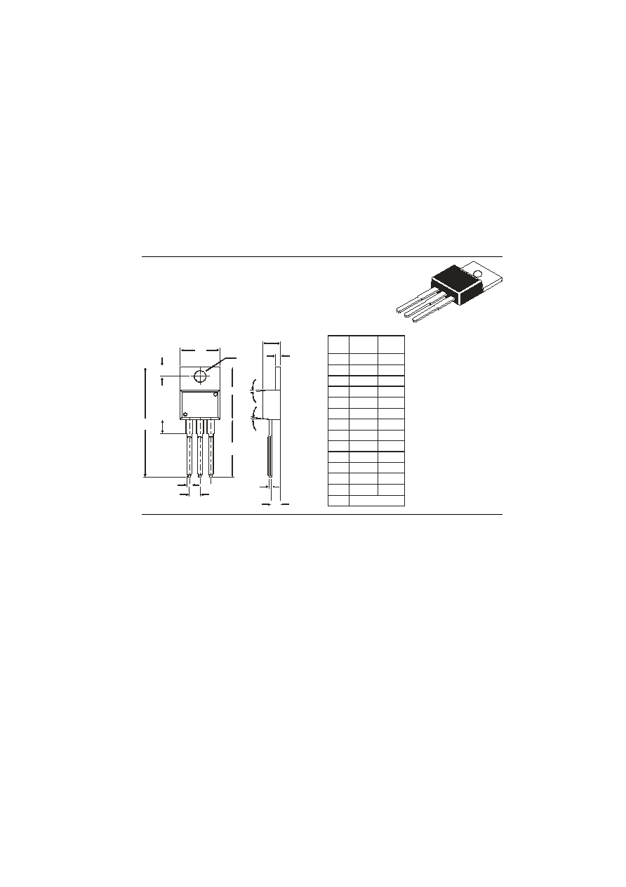
TIP41, TIP41A, TIP41B, TIP41C
TIP42, TIP42A, TIP42B, TIP42C
PIN CONFIGURATION
1. BASE
2. COLLECTOR
3. EMITTER
4. COLLECTOR
B
1 2
3
J
M
G
D
H
A
O
O
K
N
L
F
E
C
DIM
MIN .
MAX.
A
ll
d
i
min
s
io
n
s
in
m
m
.
A
14.42
16.51
B
9.63
10.67
C
3.56
4.83
D
0.90
E
1.15
1.40
F
3.75
3.88
G
2.29
2.79
H
2.54
3.43
J
0.56
K
12.70
14.73
L
2.80
4.07
M
2.03
2.92
N
31.24
O
DEG 7
1
2
3
4
IS / IECQC 700000
IS / IECQC 750100
IS/ISO 9002
Lic# QSC/L- 000019.2
Continental Device India Limited
An IS/ISO 9002 and IECQ Certified Manufacturer
TO-220 Plastic Package
http://www.bocasemi.com page: 1
Boca Semiconductor Corp (BSC)

Continental Device India Limited
Data Sheet
Page 2 of 3
Collector current (Peak value)
I
CM
max.
10
A
Base current
I
B
max.
2.0
A
Total power dissipation up to T
C
= 25∞C
P
tot
max.
65
W
Derate above 25∞C
max.
0.52
W/∞C
Total power dissipation up to T
A
= 25∞C
P
tot
max.
2.0
W
Derate above 25∞C
max.
0.016
W/∞C
Junction temperature
T
j
max.
150
∞C
Storage temperature
T
stg
≠65 to +150
∫C
THERMAL RESISTANCE
From junction to ambient
R
th j≠a
62.5
∞C/W
From junction to case
R
th j≠c
1.92
∞C/W
CHARACTERISTICS
T
amb
= 25∞C unless otherwise specified
41 41A 41B 41C
42 42A 42B 42C
Collector cutoff current
I
B
= 0; V
CE
= 30 V
I
CEO
max. 0.7
0.7
≠
≠
mA
I
B
= 0; V
CE
= 60 V
I
CEO
max. ≠
≠
0.7
0.7
mA
V
BE
= 0; V
CE
= V
CEO
I
CES
max.
0.4
mA
Emitter cut-off current
I
C
= 0; V
EB
= 5 V
I
EBO
max.
1.0
mA
Breakdown voltages
I
C
= 30 mA; I
B
= 0
V
CEO(sus)
* min. 40
60
80
100
V
I
C
= 1 mA; I
E
= 0
V
CBO
min. 40
60
80
100
V
I
E
= 1 mA; I
C
= 0
V
EBO
min.
5.0
V
Saturation voltage
I
C
= 6 A; I
B
= 0.6 A
V
CEsat
*
max.
1.5
V
Base-emitter on voltage
I
C
= 6 A; V
CE
= 4 V
V
BE(on)
*
max.
2.0
V
D.C. current gain
I
C
= 0.3 A; V
CE
= 4 V
h
FE
*
min.
30
I
C
= 3 A; V
CE
= 4 V
h
FE*
min.
15
max.
75
Small-signal current gain
I
C
= 0.5 A; V
CE
= 10 V; f = 1 KHz
|h
fe
|
min.
20
Transition frequency
I
C
= 0.5 A; V
CE
= 10 V; f = 1 MHz
f
T
min. (1)
3
MHz
* Pulse test: pulse width
300 µs, duty cycle
2%.
(1) f
T
= |h
fe
|∑ f
test
TIP41, TIP41A, TIP41B, TIP41C
TIP42, TIP42A, TIP42B, TIP42C
http://www.bocasemi.com page: 2