
Data
sheet
www.bookham.com
Thinking RF solutions
MMIC Broadband
Amplifier, 0.5 - 3.5GHz
The P35-4103-000-200 is a high performance monolithic
broadband amplifier designed for use in a wide range of
applications including telecommunications, instrumentation and
electronic warfare. The amplifier gives typically 11dB gain over
the frequency range 500MHz to 3.5 GHz. The design is self
biased, operating from a single 5 volt supply applied to the RF
output terminal through an external bias network.
The die is fabricated using Bookham Technology's F20 Gallium
Arsenide MESFET MMIC process. It is fully protected using
Silicon Nitride passivation for excellent performance and reliability.
Features
∑ Ultra Broadband
∑ Self biased. No separate gate
supply required
∑ 19dBm output power capability
∑ Input and output matched to 50
∑ Very small chip size,
1.14 x 0.76mm
www.bookham.com

www.bookham.com
Thinking RF solutions
www.bookham.com
Parameter Conditions
Min
Typ
Max
Units
Small signal gain
0.5GHz - 3.5GHz
9
11
-
dB
Gain Flatness
0.5GHz - 3.5GHz
-
±0.75
±1.0
dB
Input Return Loss
0.5GHz - 3.5GHz
9
10
-
dB
Output Return Loss
0.5GHz - 3.5GHz
11
15
-
dB
Noise figure
0.5GHz - 3.5GHz
-
3.5
4.5
dB
Output Power at 1dB compression
0.5GHz - 3.5GHz
-
19
-
dBm
Output referred IP3
2GHz - 3.5GHz
-
30
-
dBm
Supply Voltage
-
5
6
Volts
Current
Vd = 5V
60
90
105
mA
Electrical Performance
Ambient temperature = 22 ±3 Deg C , Zo = 50 ohms, Vd = 5V, Pin = -20dBm
Typical Performance at 22∞ C
Notes
1. All measurements on Wafer
Absolute maximum Ratings
Max Vds
+6.0V
Max Vgs
-5.0V
Die operating temperature -55∞C to 125∞C
Storage temperature
65∞C to +150∞
P35-4103-000-200
Gain
Noise Figure
Input Return Loss (dB)
Output Power at 1dB
Compression
Output Return Loss (dB)
www.bookham.com
462/SM/01805/200 Issue 1/2
© Bookham Technology 2003 Bookham is a registered trademark of Bookham Technology plc
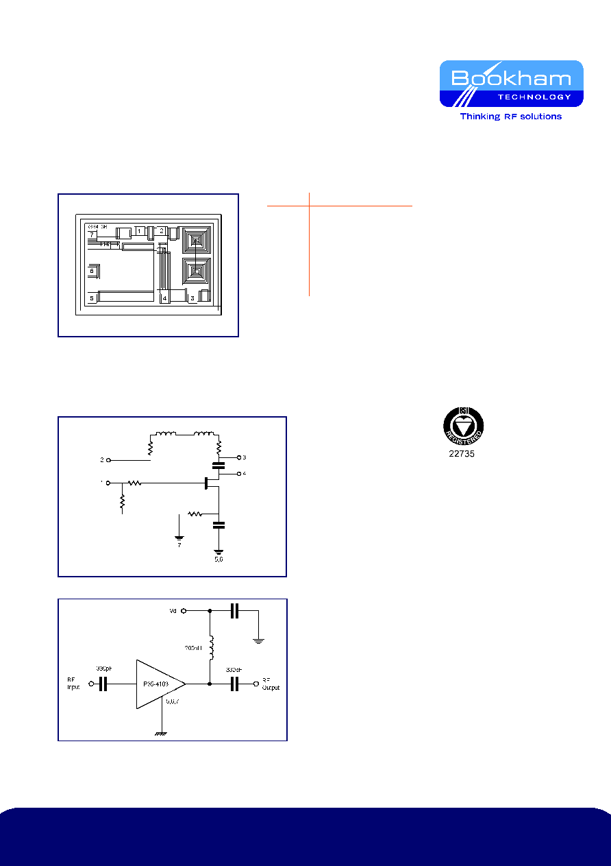
Operation
To operate the P35-4103-000-200, a drain supply of 5V is connected to the RFout via a
suitable bias circuit. Typically a 200nH inductor and 10nF decoupling capacitor can be
used. The amplifier circuit is self biased and the drain current will be typically 90mA at 5V. A
DC blocking capacitor of 330pF should be used at both the input and output. A further
blocking capacitor may be used at the output as appropriate. The ground pads must be
bonded with minimum inductance to a good DC and RF ground. It is recommended that
the die is mounted with silver loaded epoxy and bonding to all pads is with 25 µm diameter
gold wire using thermal compression bonding.
Die Outline
Pad Details
Die size: 1.143 x 0.762mm
Bond pad size: 90 µm square
Die thickness: 200 µm
Circuit Diagram
Die Bias Connections
Ordering Information
P35-4103-000-200
Pad Function
1 RF
Input
2 NC
3 NC
4
RF Output
5
GND
6
GND
7
GND
P35-4103-000-200
MMICS
Bookham Technology plc
Caswell
Towcester
Northamptonshire
NN12 8EQ
UK
∑ Tel: +44 (0) 1327 356 789
∑ Fax: +44 (0) 1327 356 698
rfsales@bookham.com
Important Notice
Bookham Technology has a policy of
continuous improvement. As a result
certain parameters detailed on this flyer
may be subject to change without notice.
If you are interested in a particular product
please request the product specification
sheet, available from any RF sales
representative.