Data
sheet
www.bookham.com
Thinking RF solutions
MMIC SPST Absorptive
Switch DC - 20GHz
The P35-4235-000-200 is a high performance Gallium
Arsenide monolithic single pole single throw broadband RF
switch. It is suitable for use in broadband communications,
instrumentation and electronic warfare applications. Control is
effected by the application of complimentary 0V and -5V levels
to the control lines in accordance with the truth table below.
The die is fabricated using Bookham Technology's 0.5 µm gate
length MESFET process (S20) and is fully protected using
Silicon Nitride passivation for excellent performance and
reliability.
Features
∑ Broadband
∑ Low insertion loss 1.8dB typ
at 18GHz
∑ Fast switching speed
∑ High isolation 50dB at 18GHz
∑ Through GaAs Vias for improved
performance
www.bookham.com
www.bookham.com
Thinking RF solutions
www.bookham.com
Electrical Performance
Ambient temperature = 22+/- 3 deg C , Zo = 50
, Gate control voltage = 0V/-5V
P35-4235-000-200
Parameter Conditions
Min
Typ
Max
Units
Insertion Loss
DC -10 GHz
-
1.4
1.6
dB
10 - 18 GHz
-
1.8
2.0
dB
18 - 20 GHz
-
1.9
2.5
dB
Isolation
DC -10 GHz
57
62
-
dB
10 - 18 GHz
50
52
-
dB
18 - 20GHz
45
50
-
dB
Input Return Loss
1
DC - 20GHz 13 17 - dB
13
17
-
dB
Output Return Loss
1
DC - 20GHz 13 17 - dB
13
17
-
dB
Input Power at 1dB compression
18
22
-
dBm
Control Voltage
-
0V/-5V
0V/-8V
Volts
Switching speed
50% control to 10%/90% RF
-
5
10
ns
Notes
1. Return loss measured in low loss state.
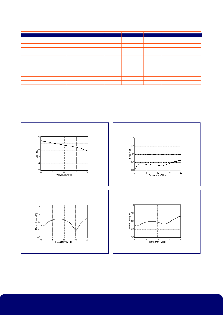
Typical Performance at 22∞ C
Insertion Loss (dB)
Isolation (dB)
Input Return Loss (dB)
Output Return Loss (dB)
Absolute Maximum Ratings
Max control voltage
-8V
Max I/P power
+25 dBm
Operating temperature
-55 ∞C to +125 ∞C
Storage temperature
-55 ∞C to +150 ∞C

Electrical Schematic
Truth Table
Pad Details
Control Line
State
3 4
J1/J2
-5V 0V
Low
Loss
0V -5V
Isolation
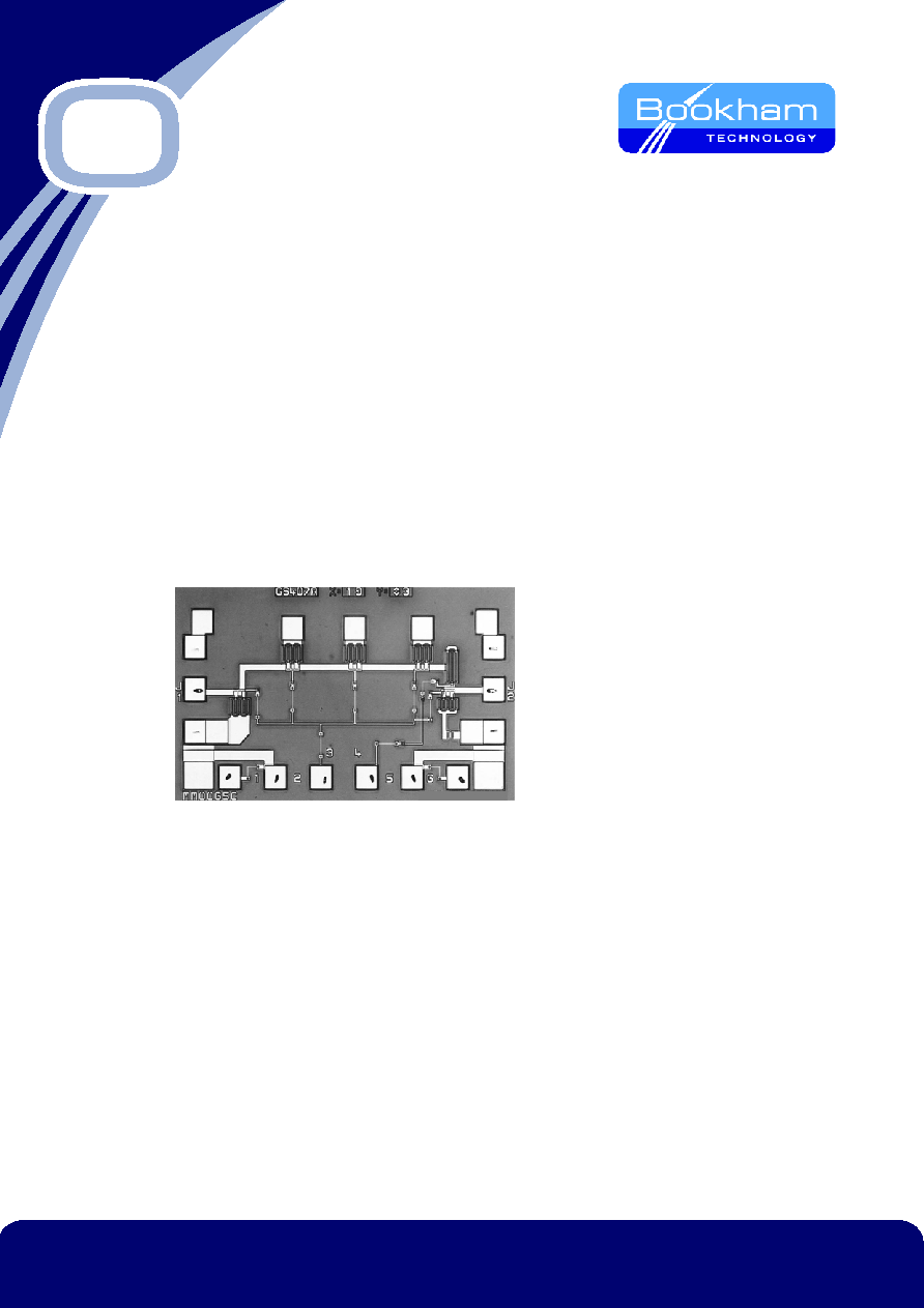
Chip Outline
Chip size:
1.91 x 1.11mm
Bond pad size:
120 µm square
Chip thickness:
200 µm
Ordering Information
P35-4235-000-200
Pad Function
J1 RF
INPUT
J2 RF
OUTPUT
1 N/C
2 N/C
3 Isolate
J1-J2
4 Enable
J1-J2
5 N/C
6 N/C
www.bookham.com
462/SM/01573/200 Issue 2
© Bookham Technology 2003 Bookham is a registered trademark of Bookham Technology plc
MMICS
Bookham Technology plc
Caswell
Towcester
Northamptonshire
NN12 8EQ
UK
∑ Tel: +44 (0) 1327 356 789
∑ Fax: +44 (0) 1327 356 698
rfsales@bookham.com
Important Notice
Bookham Technology has a policy of
continuous improvement. As a result
certain parameters detailed on this flyer
may be subject to change without notice.
If you are interested in a particular product
please request the product specification
sheet, available from any RF sales
representative.
P35-4235-000-200