Data
sheet
www.bookham.com
Thinking RF solutions
MMIC SP4T Reflective
Switch, DC - 4GHz
The P35-4250-000-200 is a high performance Gallium
Arsenide single pole four throw RF switch MMIC. It is
suitable for use in broadband communications and
instrumentation applications. A short circuit reflective
termination is presented at the isolated outputs of the
switch. The switch is controlled by the application of
complimentary 0V/-5V or 0/-8V signals to the control lines in
accordance with the truth table below.
This die is fabricated using Bookham Technology's 0.5 µm
gate length MESFET process (S20) and is fully protected
using Silicon Nitride passivation for excellent performance
and reliability.
Features
∑ Broadband performance
∑ Low insertion loss; 0.6dB typ
at 2GHz
∑ Ultra low DC power consumption
∑ Fast switching speed; 3ns typical
∑ Small die size; 0.67 mm
2
www.bookham.com

www.bookham.com
Thinking RF solutions
www.bookham.com
Electrical Performance
Ambient temperature = 22 ±3 ∞C, Zo = 50
, Control voltages = 0V/-5V unless otherwise stated
P35-4250-000-200
Parameter Conditions
Min
Typ
Max
Units
Insertion Loss
1
DC - 2GHz
-
0.6
0.9
dB
2 - 4GHz
-
0.9
0.2
dB
Isolation
1
DC - 2GHz
35
35
-
dB
2 - 4GHz
25
25
-
dB
Input Return Loss
2
DC - 2GHz
26
28
-
dB
2 - 4GHz
23
25
-
dB
Output Return Loss
2
DC - 2GHz
26
28
-
dB
2 - 4GHz
23
25
-
dB
1dB power compression point
3
0/-5V Control; 50MHz
-
19
-
dBm
0/-5V Control; 2GHz
-
22.5
-
dBm
0/-8V Control; 50MHz
-
21.5
-
dBm
0/-8V Control; 2GHz
-
30
-
dBm
Switching Speed
50% Control to 10%90%RF
-
3
-
ns
Notes
Insertion Loss and Isolation measured between RF input and any output.
1. Return Loss measured in low loss switch state.
2. Input power at which insertion loss compresses by 1dB.
Typical Performance at 22∞ C
Insertion Loss
Isolation
Input Return Loss
Output Return Loss
Absolute Maximum Ratings
Max control voltage
-8V
Max I/P power
+30dBm
Operating temperature
-60 ∞C to +125 ∞C
Storage temperature
-65 ∞C to +150 ∞C

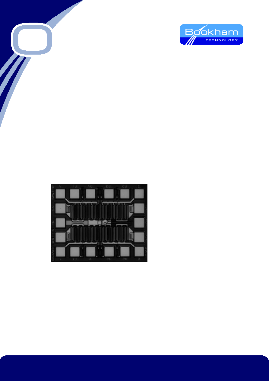
Chip Outline
Electrical Schematic
Handling, Mounting and Bonding
The back of the die is gold metallized and can be die-attached manually onto gold,
eutectically with Au- Sn (80:20) or with low temperature conductive epoxy. The
maximum allowable die temperature is 310 ∞C for 2 minutes. Bonds should be made
onto the exposed gold pads with 17 or 25 microns pure gold, half-hard gold wire.
Bonding should be achieved with the die face at 225 ∞C to 275 ∞C with a heated
thermosonic wedge (approx. 125 ∞C) and a maximum force of 60 grams. Ball bonds
may be used but care must be taken to ensure the ball size is compatible with the
bonding pads shown. The length of the bond wires should be minimised to reduce
parasitic inductance, particularly those to the RF and ground pad
Switching Truth Table
Ordering Information
P35-4250-000-200
www.bookham.com
462/SM/00027/200 Issue 1/2
© Bookham Technology 2003 Bookham is a registered trademark of Bookham Technology plc
MMICS
Bookham Technology plc
Caswell
Towcester
Northamptonshire
NN12 8EQ
UK
∑ Tel: +44 (0) 1327 356 789
∑ Fax: +44 (0) 1327 356 698
rfsales@bookham.com
Important Notice
Bookham Technology has a policy of
continuous improvement. As a result
certain parameters detailed on this flyer
may be subject to change without notice.
If you are interested in a particular product
please request the product specification
sheet, available from any RF sales
representative.
P35-4250-000-200
Chip Outline Die size: 0.91 x 0.74mm
Bond pad size:
90 µm x 90 µm
Die thickness:
200 µm
Control Pad Voltage (V)
Path From RF IN to
A1 B1 A2 B2
A3 B3 A4 B4
RF1
RF2
RF3
RF4
-5 0 0 -5 0 -5 0 -5 Low
Loss
Isolated
Isolated Isolated
0 -5 -5 0 0 -5 0 -5 Isolated
Low
Loss
Isolated Isolated
0 -5 0
-5 -5 0
0 -5
Isolated Isolated
Low
Loss Isolated
0 -5 0 -5 0 -5 -5 0
Isolated
Isolated
Isolated
Low
Loss