 | –≠–ª–µ–∫—Ç—Ä–æ–Ω–Ω—ã–π –∫–æ–º–ø–æ–Ω–µ–Ω—Ç: P35-5146 | –°–∫–∞—á–∞—Ç—å:  PDF PDF  ZIP ZIP |

Data
sheet
www.bookham.com
Thinking RF solutions
HEMT MMIC Broadband
Amplifier, 30KHz - 20GHz
The P35-5146-000-200 is a high performance 30KHz -
20GHz Gallium Arsenide broadband driver amplifier. This
product is intended for use as an optical driver amplifier in
fibre optic systems or as a medium power amplifier for
broadband communication systems.
The die is fabricated using Bookham Technology's 0.20µm
gate length, pHEMT process and is fully protected using
Silicon Nitride passivation for excellent performance and
reliability.
Features
∑ >22dBm Typical Saturated
Output Power
∑ High Gain 12dB Typical
∑ Small 1.67 x 1.14mm Die Size
∑ Flat Gain response ± 0.5dB
to 10GHz Typical
∑ Output Voltage typically >7.5V
Peak-to Peak
www.bookham.com
Engineering Datasheet
www.bookham.com
Thinking RF solutions
www.bookham.com
Parameter
Conditions Min
Typ
Max
Units
Small Signal Gain
30KHz ≠ 20GHz
-
13
-
dB
Small Signal Gain Flatness
30KHz ≠ 20GHz
-
± 1
-
dB
Input Return Loss
30KHz ≠ 20GHz
-
12
-
dB
Output Return Loss
30KHz ≠ 20GHz
-
10
-
dB
Output Power @P1dB
Vdd 8V
-
22
-
dBm
Saturated Output Power
-
23
-
dBm
Drain Voltage Vdd
-
8.0
-
V
Gate Voltage Vgg
-
-3.0
-
V
Total Current Idd
-
100
-
mA
Electrical Performance
Ambient Temperature 22±3∫C, Zo = 50
, Vdd = 8V, Vg1 = -3.0V
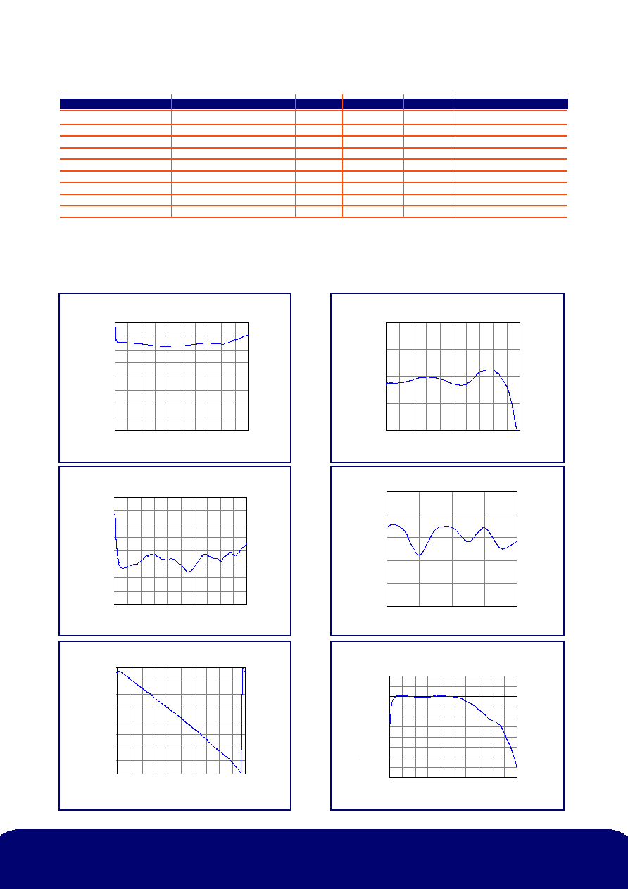
Output Power @ 1dB compression
18
20
22
24
26
28
2
4
6
8
10
Frequency (GHz)
Pout (dBm)
P35-5146-000-200
Notes
1. All Measurements RFOW
Output Return Loss
0
5
10
15
20
25
30
35
40
0
2
4
6
8
10 12 14 16 18 20
Frequency (GHz)
Return Loss (dB)
Deviation from Linear phase
Least Squares fit 1-10GHz
-40
-35
-30
-25
-20
-15
-10
-5
0
5
10
0
2
4
6
8 10 12 14 16 18 20
Frequency (GHz)
S21 (Degrees)
S21 Phase
-180
-135
-90
-45
0
45
90
135
180
0
2
4
6
8
10 12 14 16 18 20
Frequency (GHz)
S21 (Degrees)
Gain
0
2
4
6
8
10
12
14
16
0
2
4
6
8
10 12 14 16 18 20
Frequency (GHz)
Gain (dB)
Input Return Loss
0
5
10
15
20
0
2
4
6
8
10 12 14 16 18 20
Frequency (GHz)
Return Loss (dB)
Typical RFOW Performance

P35-5146-000-200
www.bookham.com
462/SM/XXXXX/200 Issue 1
© Bookham Technology 2003 Bookham is a registered trademark of Bookham Technology plc
MMICS
Bookham Technology plc
Caswell
Towcester
Northamptonshire
NN12 8EQ
UK
∑ Tel: +44 (0) 1327 356 789
∑ Fax: +44 (0) 1327 356 698
rfsales@bookham.com
Important Notice
Bookham Technology has a policy of
continuous improvement. As a result
certain parameters detailed on this flyer
may be subject to change without notice.
If you are interested in a particular product
please request the product specification
sheet, available from any RF sales
representative.
The P35-5146-000-200 uses a fixed Vdd of +8V and a fixed Vgg of ≠3V, the input and
output are both DC coupled. For low frequency operation an external bypass
capacitors >0.1uF is required at pad 2. The drain supply Vdd needs to be applied via
an external inductor
Chip Outline
Die Details
Die size:
1.67 x 1.14mm
RF bond pads (1 & 4):
120
m x 120m
All other bond pads:
120
m x 120m
Die Thickness:
100
m
Ordering Information
P35-5146-000-200
Pad Details
Pad
Function
1
RF Input
2
By Pass Capacitor
3
Vdd (8V)
4
RF Output
5
Vgg (-3V)
6
N/C