 | –≠–ª–µ–∫—Ç—Ä–æ–Ω–Ω—ã–π –∫–æ–º–ø–æ–Ω–µ–Ω—Ç: 2FAA-M20R | –°–∫–∞—á–∞—Ç—å:  PDF PDF  ZIP ZIP |

2FAA-M20R ≠ Integrated Passive & Active Device using MLP
Specifications are subject to change without notice.
Customers should verify actual device performance in their specific applications.
I/O PADS
GROUND
PAD
MLP
PACKAGE
General Information
Features
Lead free as standard
RoHS compliant*
ESD protection
Protects up to ten data lines
Low insertion loss
Applications
Cell Phones
PDAs and Notebooks
GPS and SMART Cards
The 2FAA-M20R device, manufactured using Thin Film on
Silicon technology, provides ESD protection for the external
ports of portable electronic devices such as cell phones,
modems and PDAs.
The ESD protection provided by the component enables a
data port to withstand a minimum ±8 KV Contact /±15 KV Air
Discharge per the ESD test method specified in IEC 61000-4-2.
The device measures 3.5 mm x 3.5 mm and is intended to be
mounted directly onto an FR4 printed circuit board. The MLP
device meets typical thermal cycle and bend test specifications.
Electrical Characteristics
Symbol
Minimum
Nominal
Maximum
Unit
(T
A
= 25 ∞C unless otherwise noted)
Resistance
R
180
200
220
Capacitance @ 2.5 V 1 MHz
C
16
20
24
pF
Rated Standoff Voltage
V
WM
5.0
V
Breakdown Voltage @ 1 mA
V
BR
6.0
V
Forward Voltage @ 10 mA
V
F
0.8
V
Leakage Current @ 3 V
I
D
0.1
µA
ESD Protection: IEC 61000-4-2
Contact Discharge
±8
kV
Air Discharge
±15
kV
Thermal Characteristics
(T
A
= 25 ∞C unless otherwise noted)
DC Power Rating
P
100
mW
Operating Temperature Range
T
J
-40 25 +85 ∞C
Storage Temperature Range
T
STG
-55 25 +150 ∞C
Electrical & Thermal Characteristics
*RoHS COMPLIANT
*RoHS Directive 2002/95/EC Jan 27 2003 including Annex

Specifications are subject to change without notice.
Customers should verify actual device performance in their specific applications.
Product Dimensions
Recommended Pad Layout
2FAA-M20R ≠ Integrated Passive & Active Device using MLP
How to Order
2 FAA ≠ M 20 R
Thin Film
Model
MLP Package
No. of Solder Pads
Packaging Option
R = Tape and Reel
Packaged 3000 pcs. / 13 reel
(100 % Sn Termination)
FAA
B0412
3.51
(0.138)
2.01
(0.0790)
0.43
(0.0170)
0.27
(0.0106)
3.51
(0.138)
0.75
(0.0295)
3.51
(0.138)
2.03
(0.080)
0.75
(0.0295)
3.51
(0.138)
0.5
(0.020)
0.40
(0.016)
3.51
(0.138)
2.01
(0.079)
0.51
(0.020)
This silicon-based device is packaged using micro leadframe
packaging technology. The MLPs have an exposed die attach
pad that provides the interconnect medium from die to PCB.
The pads are arranged for easy PCB routing. The pitch is
0.5 mm and the dimensions for the packaged device are
shown below.
DIMENSIONS =
MILLIMETERS
(INCHES)
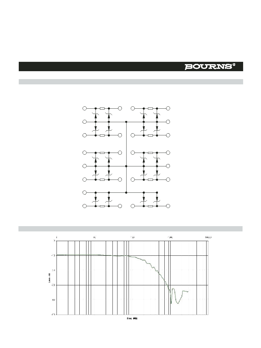
Block Diagram
2FAA-M20R ≠ Integrated Passive & Active Device using MLP
GND
EXT3
R3
R4
INT3
EXT4
INT5
GND
EXT8
R8
R7
INT8
EXT7
INT7
GND
R5
EXT5
INT5
R6
EXT6
INT6
GND
EXT1
R1
R2
INT1
EXT2
INT2
GND
EXT10
R10
R9
INT10
EXT9
INT9
The MLP Device block diagram below includes the pin names and basic electrical connections associated with each channel.
Frequency Response
Specifications are subject to change without notice.
Customers should verify actual device performance in their specific applications.

2FAA-M20R ≠ Integrated Passive & Active Device using MLP
Specifications are subject to change without notice.
Customers should verify actual device performance in their specific applications.
Device Pin Out
1
EXT3
2
EXT2
3
EXT1
4
INT1
5
INT2
15
EXT9
14
EXT10
13
INT10
12
INT9
11
INT8
6
INT3
7
INT4
8
INT5
9
INT6
10
INT7
20
EXT4
19
EXT5
18
EXT7
17
EXT7
16
EXT8
The Pin-Out for the device is shown below. Note also that the device is shown with bottom side pads facing up.
Packaging
The surface mount product is packaged in a 12 mm x 8 mm Tape and Reel format per EIA-481 standard.
COPYRIGHT© 2004, BOURNS, INC. LITHO IN U.S.A. 06/05 e/IPA0507
2FAA-M20R REV. A 03/05
Asia-Pacific:
TEL +886- (0)2 25624117 ∑ FAX +886- (0)2 25624116
Europe:
TEL +41-41 768 5555 ∑ FAX +41-41 768 5510
The Americas: TEL +1-951 781-5492 ∑ FAX +1-951 781-5700
www.bourns.com
Reliable Electronic Solutions
Pin Out Function Pin Out Function Pin Out Function
Pin Out
Function
Pin1
EXT3
Pin6
INT3
Pin11
INT8
Pin16
EXT8
Pin2
EXT2
Pin7
INT4
Pin12
INT9
Pin17
EXT7
Pin3
EXT1
Pin8
INT5
Pin13
INT10
Pin18
EXT6
Pin4
INT1
Pin9
INT6
Pin14
EXT10
Pin19
EXT5
Pin5
INT2
Pin10
INT7
Pin15
EXT9
Pin20
EXT4
2.0 ± 0.05
(.08 ± .002)
0.3 ± 0.05
(.01 ± .002)
3.9 ± 0.1
(.154 ± .004)
3.9 ± 0.1
(.154 ± .004)
1.75 ± 0.1
(.07 ± .004)
5.5 ± 0.3
(.22 ± .01)
12.0 ± 0.3
(.47 ± .01)
0.9 ± 0.1
(.035 ± .004)
ORIENTATION
OF COMPONENT
IN POCKET
BACKSIDE FACING UP
TOP SIDE VIEW
(INTO COMPONENT POCKET)
0.3
(0.01)
4.0 ± 0.1
(.16 ± .004)
8.0 ± 0.3
(.31 ± .01)
0.25
(0.010)
TYP.
R
1.5 ± 0.1/-0
(.06 ± .004/-0)
DIA.
MAX.
R
DIMENSIONS =
MILLIMETERS
(INCHES)