 | –≠–ª–µ–∫—Ç—Ä–æ–Ω–Ω—ã–π –∫–æ–º–ø–æ–Ω–µ–Ω—Ç: BU47 | –°–∫–∞—á–∞—Ç—å:  PDF PDF  ZIP ZIP |
BUV47, BUV47A
NPN SILICON POWER TRANSISTORS
P R O D U C T
I N F O R M A T I O N
1
AUGUST 1978 - REVISED SEPTEMBER 2002
Specifications are subject to change without notice.
Rugged Triple-Diffused Planar Construction
9 A Continuous Collector Current
1000 Volt Blocking Capability
absolute maximum ratings at 25∞C case temperature (unless otherwise noted)
NOTE
1: This value applies for t
p
5 ms, duty cycle 2%.
RATING
SYMBOL
VALUE
UNIT
Collector-emitter voltage (V
BE
= -2.5 V)
BUV47
BUV47A
V
CEX
850
1000
V
Collector-emitter voltage (R
BE
= 10
)
BUV47
BUV47A
V
CER
850
1000
V
Collector-emitter voltage (I
B
= 0)
BUV47
BUV47A
V
CEO
400
450
V
Continuous collector current
I
C
9
A
Peak collector current (see Note 1)
I
CM
15
A
Continuous base current
I
B
3
A
Peak base current
I
BM
6
A
Continuous device dissipation at (or below) 25∞C case temperature
P
tot
120
W
Operating junction temperature range
T
j
-65 to +150
∞C
Storage temperature range
T
stg
-65 to +150
∞C
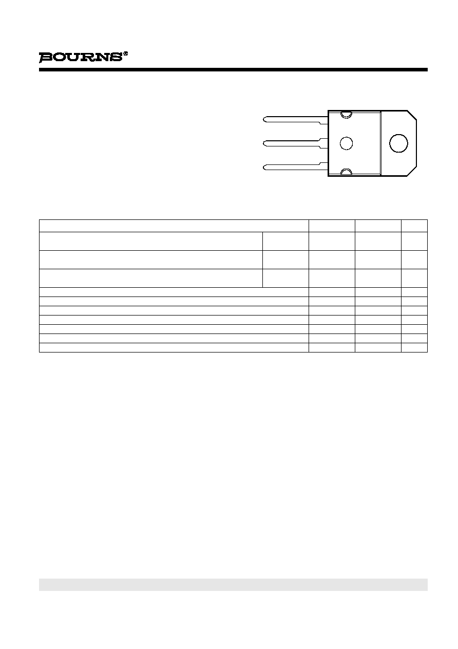
SOT-93 PACKAGE
(TOP VIEW)
Pin 2 is in electrical contact with the mounting base.
MDTRAAA
B
C
E
1
2
3
BUV47, BUV47A
NPN SILICON POWER TRANSISTORS
2
P R O D U C T
I N F O R M A T I O N
AUGUST 1978 - REVISED SEPTEMBER 2002
Specifications are subject to change without notice.
NOTES: 2. Inductive loop switching measurement.
3. These parameters must be measured using pulse techniques, t
p
= 300 µs, duty cycle
2%.
4. These parameters must be measured using voltage-sensing contacts, separate from the current carrying contacts.
Voltage and current values shown are nominal; exact values vary slightly with transistor parameters.
electrical characteristics at 25∞C case temperature (unless otherwise noted)
PARAMETER
TEST CONDITIONS
MIN
TYP
MAX
UNIT
V
CEO(sus)
Collector-emitter
sustaining voltage
I
C
= 200 mA
L = 25 mH
(see Note 2)
BUV47
BUV47A
400
450
V
V
(BR)EBO
Base-emitter
breakdown voltage
I
E
= 50 mA
I
C
= 0
(see Note 3)
7
30
V
I
CES
Collector-emitter
cut-off current
V
CE
= 850 V
V
CE
= 1000 V
V
CE
= 850 V
V
CE
= 1000 V
V
BE
= 0
V
BE
= 0
V
BE
= 0
V
BE
= 0
T
C
= 125∞C
T
C
= 125∞C
BUV47
BUV47A
BUV47
BUV47A
0.15
0.15
1.5
1.5
mA
I
CER
Collector-emitter
cut-off current
V
CE
= 850 V
V
CE
= 1000 V
V
CE
= 850 V
V
CE
= 1000 V
R
BE
= 10
R
BE
= 10
R
BE
= 10
R
BE
= 10
T
C
= 125∞C
T
C
= 125∞C
BUV47
BUV47A
BUV47
BUV47A
0.4
0.4
3.0
3.0
mA
I
EBO
Emitter cut-off
current
V
EB
= 5 V
I
C
= 0
1
mA
V
CE(sat)
Collector-emitter
saturation voltage
I
B
= 1 A
I
B
= 2.5 A
I
C
= 5A
I
C
= 8A
(see Notes 3 and 4)
1.5
3.0
V
V
BE(sat)
Base-emitter
saturation voltage
I
B
= 1 A
I
C
= 5A
(see Notes 3 and 4)
1.6
V
f
t
Current gain
bandwidth product
V
CE
= 10 V
I
C
= 0.5 A
f = 1 MHz
8
MHz
C
ob
Output capacitance
V
CB
= 20 V
I
C
= 0
f = 0.1 MHz
105
pF
thermal characteristics
PARAMETER
MIN
TYP
MAX
UNIT
R
JC
Junction to case thermal resistance
1
∞C/W
resistive-load-switching characteristics at 25∞C case temperature
PARAMETER
TEST CONDITIONS
MIN
TYP
MAX
UNIT
t
on
Turn on time
I
C
= 5 A
V
CC
= 150 V
I
B(on)
= 1 A
(see Figures 1 and 2)
I
B(off)
= -1 A
1.0
µs
t
s
Storage time
3.0
µs
t
f
Fall time
0.8
µs
inductive-load-switching characteristics at 25∞C case temperature (unless otherwise noted)
PARAMETER
TEST CONDITIONS
MIN
TYP
MAX
UNIT
t
sv
Voltage storage time
I
C
= 5 A
T
C
= 100∞C
I
B(on)
= 1 A
(see Figures 3 and 4)
V
BE(off)
= -5 V
4.0
µs
t
fi
Current fall time
0.4
µs

BUV47, BUV47A
NPN SILICON POWER TRANSISTORS
3
P R O D U C T
I N F O R M A T I O N
AUGUST 1978 - REVISED SEPTEMBER 2002
Specifications are subject to change without notice.
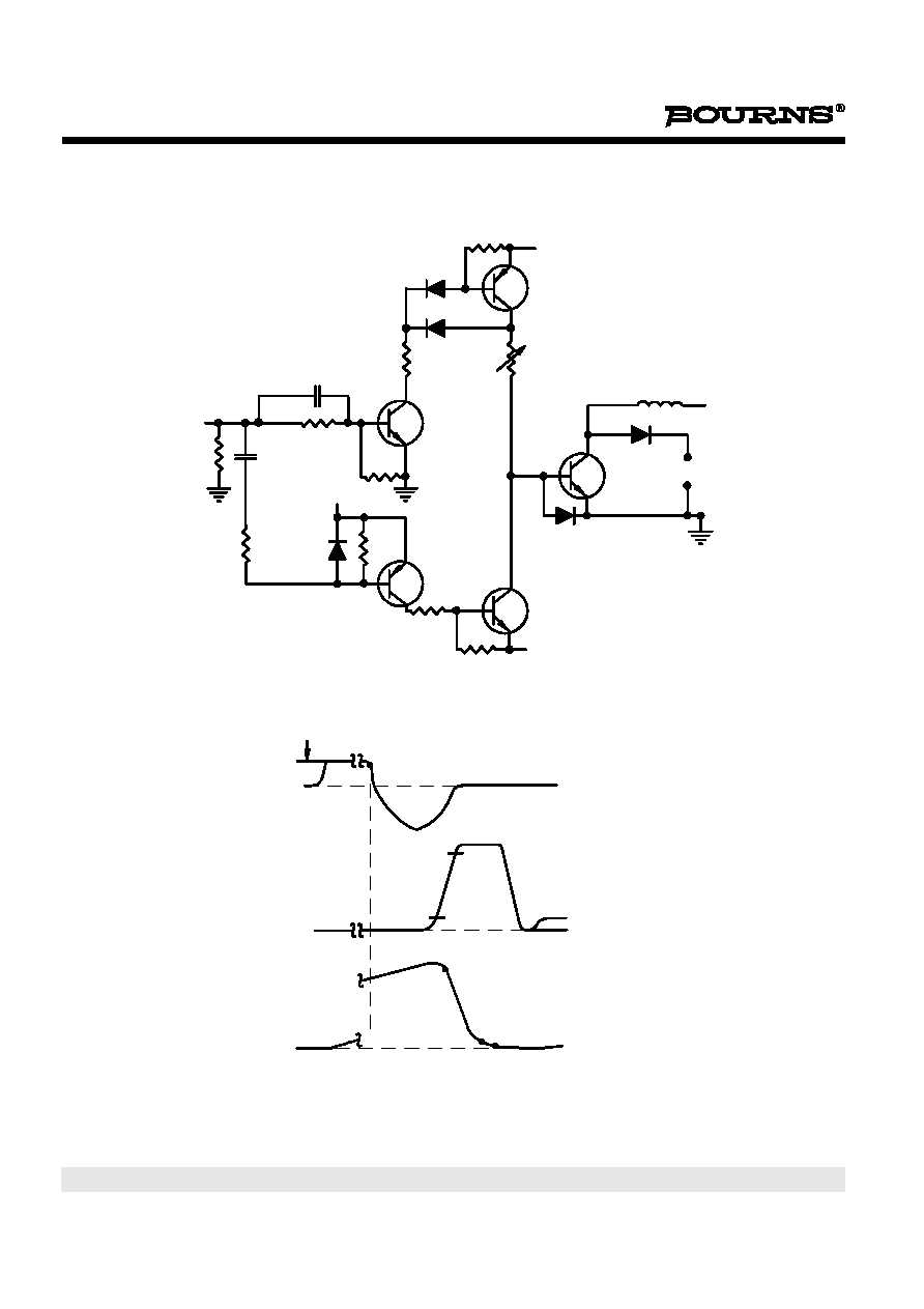
PARAMETER MEASUREMENT INFORMATION
Figure 1. Resistive-Load Switching Test Circuit
Figure 2. Resistive-Load Switching Waveforms
tp
F
µ
100
V
1
680
F
µ
V1
V cc = 250 V
+25 V
BD135
47
100
120
15
82
100
BD136
680
F
µ
TUT
T
t
p
= 20
µs
Duty cycle = 1%
V
1
= 15 V, Source Impedance = 50
V
CC
0%
C
B
90%
10%
A
10%
90%
10%
90%
E
F
D
I B
IC
I
B(on)
I B(off)
0%
dI
B
dt
2 A/µs
A - B = t
d
B - C = t
r
E - F = t
f
D - E = t
s
A - C = t
on
D - F = t
off
BUV47, BUV47A
NPN SILICON POWER TRANSISTORS
4
P R O D U C T
I N F O R M A T I O N
AUGUST 1978 - REVISED SEPTEMBER 2002
Specifications are subject to change without notice.
PARAMETER MEASUREMENT INFORMATION
Figure 3. Inductive-Load Switching Test Circuit
Figure 4. Inductive-Load Switching Waveforms
RB
(on)
V
BE(off)
Vclamp = 400 V
vcc
µH
180
33
+5V
D45H11
BY205-400
BY205-400
2N2222
BY205-400
5X BY205-400
BY205-400
1 k
68
1 k
47
2N2904
D44H11
100
270
V Gen
+5V
1 k
0.02
µF
TUT
1 pF
33
Adjust pw to obtain I
C
For I
C
< 6 A V
CC
= 50 V
For I
C
6 A V
CC
= 100 V
Base Current
A (90%)
I
B(on)
IB
Collector Voltage
Collector Current
D (90%)
E (10%)
F (2%)
C
B
90%
10%
V
CE
I
C(on)
A - B = t
sv
B - C = t
rv
D - E = t
fi
E - F = t
ti
B - E = t
xo
NOTES: A. Waveforms are monitored on an oscilloscope with the following characteristics: t
r
< 15 ns, R
in
> 10
, C
in
< 11.5 pF.
B. Resistors must be noninductive types.

BUV47, BUV47A
NPN SILICON POWER TRANSISTORS
5
P R O D U C T
I N F O R M A T I O N
AUGUST 1978 - REVISED SEPTEMBER 2002
Specifications are subject to change without notice.
TYPICAL CHARACTERISTICS
Figure 5.
Figure 6.
Figure 7.
Figure 8.
TYPICAL DC CURRENT GAIN
vs
COLLECTOR CURRENT
I
C
- Collector Current - A
0∑1
1∑0
10
h
FE
-
T
y
p
i
ca
l
D
C
C
u
rre
n
t
G
a
i
n
1∑0
10
100
TCP762AA
V
CE
= 5 V
T
C
= 125∞C
T
C
= 25∞C
T
C
= -65∞C
COLLECTOR-EMITTER SATURATION VOLTAGE
vs
BASE CURRENT
I
B
- Base Current - A
0
0∑5
1∑0
1∑5
2∑0
2∑5
V
C
E
(
sat
)
- Co
l
l
e
c
to
r-Em
i
tte
r Sa
tu
ra
ti
o
n
Vo
l
t
a
g
e
- V
0
1∑0
2∑0
3∑0
4∑0
5∑0
TCP762AB
I
C
= 8 A
I
C
= 6 A
I
C
= 4 A
I
C
= 2 A
T
C
= 25∞C
COLLECTOR-EMITTER SATURATION VOLTAGE
vs
BASE CURRENT
I
B
- Base Current - A
0
0∑5
1∑0
1∑5
2∑0
2∑5
V
C
E
(
sat
)
- Co
l
l
e
c
to
r-Em
i
tte
r Sa
tu
ra
ti
o
n
Vo
l
t
a
g
e
- V
0
0∑1
0∑2
0∑3
0∑4
0∑5
TCP762AK
T
C
= 100∞C
I
C
= 8 A
I
C
= 6 A
I
C
= 4 A
I
C
= 2 A
COLLECTOR CUT-OFF CURRENT
vs
CASE TEMPERATURE
T
C
- Case Temperature - ∞C
-80 -60 -40 -20
0
20
40
60
80 100 120 140
I
CE
S
- Co
l
l
e
c
to
r Cu
t-o
ff Cu
rre
n
t - µ
A
0∑001
0∑01
0∑1
1∑0
10
TCP762AC
BUV47A
V
CE
= 1000 V
BUV47
V
CE
= 850 V