 | –≠–ª–µ–∫—Ç—Ä–æ–Ω–Ω—ã–π –∫–æ–º–ø–æ–Ω–µ–Ω—Ç: BUT11 | –°–∫–∞—á–∞—Ç—å:  PDF PDF  ZIP ZIP |

BUT11
NPN SILICON POWER TRANSISTOR
P R O D U C T
I N F O R M A T I O N
1
MAY 1989 - REVISED SEPTEMBER 2002
Specifications are subject to change without notice.
Rugged Triple-Diffused Planar Construction
100 W at 25∞C Case Temperature
5 A Continuous Collector Current
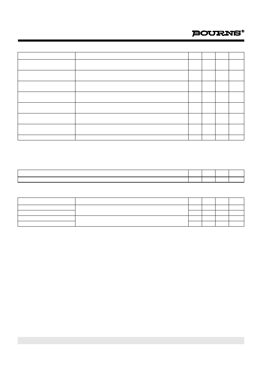
absolute maximum ratings at 25∞C case temperature (unless otherwise noted)
NOTE
1: This value applies for t
p
10 ms, duty cycle 2%.
RATING
SYMBOL
VALUE
UNIT
Collector-base voltage (I
E
= 0)
V
CBO
850
V
Collector-emitter voltage (V
BE
= 0)
V
CES
850
V
Collector-emitter voltage (I
B
= 0)
V
CEO
400
V
Emitter-base voltage
V
EBO
10
V
Continuous collector current
I
C
5
A
Peak collector current (see Note 1)
I
CM
10
A
Continuous device dissipation at (or below) 25∞C case temperature
P
tot
100
W
Operating junction temperature range
T
j
-65 to +150
∞C
Storage temperature range
T
stg
-65 to +150
∞C
B
C
E
TO-220 PACKAGE
(TOP VIEW)
Pin 2 is in electrical contact with the mounting base.
MDTRACA
1
2
3
BUT11
NPN SILICON POWER TRANSISTOR
2
P R O D U C T
I N F O R M A T I O N
MAY 1989 - REVISED SEPTEMBER 2002
Specifications are subject to change without notice.
NOTES: 2. Inductive loop switching measurement.
3. These parameters must be measured using pulse techniques, t
p
= 300 µs, duty cycle
2%.
4. These parameters must be measured using voltage-sensing contacts, separate from the current carrying contacts.
Voltage and current values shown are nominal; exact values vary slightly with transistor parameters.
electrical characteristics at 25∞C case temperature (unless otherwise noted)
PARAMETER
TEST CONDITIONS
MIN
TYP
MAX
UNIT
V
CEO(sus)
Collector-emitter
sustaining voltage
I
C
= 0.1 A
L = 25 mH
(see Note 2)
400
V
I
CES
Collector-emitter
cut-off current
V
CE
= 850 V
V
CE
= 850 V
V
BE
= 0
V
BE
= 0
T
C
= 125∞C
50
500
µA
I
EBO
Emitter cut-off
current
V
EB
= 10 V
I
C
= 0
1
mA
h
FE
Forward current
transfer ratio
V
CE
= 5 V
I
C
= 0.5 A
(see Notes 3 and 4)
20
60
V
CE(sat)
Collector-emitter
saturation voltage
I
B
= 0.6 A
I
C
= 3 A
(see Notes 3 and 4)
1.5
V
V
BE(sat)
Base-emitter
saturation voltage
I
B
= 0.6 A
I
C
= 3 A
(see Notes 3 and 4)
1.3
V
f
t
Current gain
bandwidth product
V
CE
= 10 V
I
C
= 0.5 A
f = 1 MHz
12
MHz
C
ob
Output capacitance
V
CB
= 20 V
I
E
= 0
f = 0.1 MHz
110
pF
thermal characteristics
PARAMETER
MIN
TYP
MAX
UNIT
R
JC
Junction to case thermal resistance
1.25
∞C/W
inductive-load-switching characteristics at 25∞C case temperature (unless otherwise noted)
PARAMETER
TEST CONDITIONS
MIN
TYP
MAX
UNIT
t
sv
Voltage storage time
I
C
= 3 A
V
CC
= 50 V
I
B(on)
= 0.6A
(see Figures 1 and 2)
V
BE(off)
= -5 V
1.4
µs
t
fi
Current fall time
150
ns
t
sv
Voltage storage time
I
C
= 3 A
V
CC
= 50 V
I
B(on)
= 0.6A
T
C
= 100∞C
V
BE(off)
= -5 V
1.5
µs
t
fi
Current fall time
300
ns

BUT11
NPN SILICON POWER TRANSISTOR
3
P R O D U C T
I N F O R M A T I O N
MAY 1989 - REVISED SEPTEMBER 2002
Specifications are subject to change without notice.
PARAMETER MEASUREMENT INFORMATION
Figure 1. Inductive-Load Switching Test Circuit
Figure 2. Inductive-Load Switching Waveforms
RB
(on)
V
BE(off)
Vclamp = 400 V
vcc
µH
180
33
+5V
D45H11
BY205-400
BY205-400
2N2222
BY205-400
5X BY205-400
BY205-400
1 k
68
1 k
47
2N2904
D44H11
100
270
V Gen
+5V
1 k
0.02
µF
TUT
1 pF
33
Adjust pw to obtain I
C
For I
C
< 6 A V
CC
= 50 V
For I
C
6 A V
CC
= 100 V
Base Current
A (90%)
I
B(on)
IB
Collector Voltage
Collector Current
D (90%)
E (10%)
F (2%)
C
B
90%
10%
V
CE
I
C(on)
A - B = t
sv
B - C = t
rv
D - E = t
fi
E - F = t
ti
B - E = t
xo
NOTES: A. Waveforms are monitored on an oscilloscope with the following characteristics: t
r
< 15 ns, R
in
> 10
, C
in
< 11.5 pF.
B. Resistors must be noninductive types.

BUT11
NPN SILICON POWER TRANSISTOR
4
P R O D U C T
I N F O R M A T I O N
MAY 1989 - REVISED SEPTEMBER 2002
Specifications are subject to change without notice.
MAXIMUM SAFE OPERATING REGIONS
Figure 3.
MAXIMUM FORWARD-BIAS
SAFE OPERATING AREA
V
CE
- Collector-Emitter Voltage - V
1∑0
10
100
1000
I
C
- Co
l
l
e
c
to
r Cu
rre
n
t
- A
0∑01
0.1
1∑0
10
100
SAP791AB
t
p
= 10
µs
t
p
= 100
µs
t
p
= 1 ms
t
p
= 10 ms
DC Operation

BUT11
NPN SILICON POWER TRANSISTOR
5
P R O D U C T
I N F O R M A T I O N
MAY 1989 - REVISED SEPTEMBER 2002
Specifications are subject to change without notice.
TO-220
3-pin plastic flange-mount package
This single-in-line package consists of a circuit mounted on a lead frame and encapsulated within a plastic
compound. The compound will withstand soldering temperature with no deformation, and circuit performance
characteristics will remain stable when operated in high humidity conditions. Leads require no additional
cleaning or processing when used in soldered assembly.
MECHANICAL DATA
TO220
ALL LINEAR DIMENSIONS IN MILLIMETERS
¯
1,23
1,32
4,20
4,70
1
2
3
0,97
0,61
see Note C
see Note B
10,0
10,4
2,54
2,95
6,0
6,6
14,55
15,90
12,7
14,1
3,5
6,1
1,07
1,70
2,34
2,74
4,88
5,28
3,71
3,96
0,41
0,64
2,40
2,90
VERSION 2
VERSION 1
NOTES: A. The centre pin is in electrical contact with the mounting tab.
B. Mounting tab corner profile according to package version.
C. Typical fixing hole centre stand off height according to package version.
Version
1,
18.0
mm.
Version
2,
17.6
mm.
MDXXBE