Switching Chip Diode Series - 0805 / 1206
*RoHS Directive 2002/95/EC Jan 27 2003 including Annex
Specifications are subject to change without notice.
Customers should verify actual device performance in their specific applications.
6
Features
Lead free as standard
RoHS compliant*
Leadless
High speed
Applications
Cellular phones
PDAs
Desktop PCs and
notebooks
Digital cameras
MP3 players
General Information
The markets of portable communications, computing and video equipment are challenging the semiconductor industry to develop increasingly
smaller electronic components.
Bourns offers small-signal high-speed Switching Diodes for switching digital signal applications, in compact chip package 0805 and 1206 size
format, which offer PCB real estate savings and are considerably smaller than competitive parts. The Switching Diodes offer a forward current
of 100 mA or 150 mA, a reverse voltage of 80 V or 75 V and also have a low leakage reverse current option. The diodes are lead-free with
Cu/Ni/Au plated terminations and are compatible with lead-free manufacturing processes, conforming to many industry and government
regulations on lead-free components.
Bourns
Æ
Chip Diodes conform to JEDEC standards, easy to handle on standard pick and place equipment and their flat configuration makes
roll away much more difficult.
Parameter
Symbol
CDxxxx-S0180
CDxxxx-S01575
CDxxxx-S0180R
Unit
Forward Voltage (Max.)
VF
1.00
1.00
1.00
V
(If = 100 mA)
(If = 50 mA)
(If = 100 mA)
Capacitance Between Terminals (Max.)
CT
3
pF
(f = 100 MHz, Vr = 1 V DC)
Reverse Recovery Time (Max.)
trr
4
nS
(Vr = 6V, If = 10 mA, RL = 50 )
Reverse Current (Max.)
IR
0.1
2.5
0.05
µA
(Vr = 80 V)
(Vr = 75 V)
(Vr = 75 V)
Electrical Characteristics (@ TA = 25 ∞C Unless Otherwise Noted)
Parameter
Symbol
CDxxxx-S0180
CDxxxx-S01575
CDxxxx-S0180R
Unit
Repetitive Peak Reverse Voltage
VRRM
90
100
90
V
Reverse Voltage
VR
80
75
80
V
Average Forward Current
Io
100
150
100
mA
Forward Current, Surge Peak
Isurge
1*
4**
1*
A
Power Dissipation
PD
300
350
300
mW
Storage Temperature
TSTG
-55 to +125
∞C
Junction Temperature
TJ
-55 to +125
∞C
Absolute Ratings (@ TA = 25 ∞C Unless Otherwise Noted)
* Condition: 8.3 ms single half sine-wave superimposed on rate load
(JEDEC method).
** Condition: 1.0 µs single half sine-wave superimposed on rate load
(JEDEC method).
How To Order
CD 0805 - S 01 80 R
Common Code
Chip Diode
Package
∑ 0805
∑ 1206
Model
S = High Speed Switching
Average Forward Current (Io) Code
01 = 100 mA
015 = 150 mA
(Code x 1000 mA = Average Forward Current)
Reverse Voltage (VR) Code
80 = 80 V
75 = 75 V
Reverse Current Suffix
R = Low Leakage IR (CDxxxx-S0180R)
*RoHS COMPLIANT
CD0805-xxxx products
are currently available,
although not recom-
mended for new designs. Use
CD1005-xxxx
products as an
alternative.
Specifications are subject to change without notice.
Customers should verify actual device performance in their specific applications.
Switching Chip Diode Series - 0805 / 1206
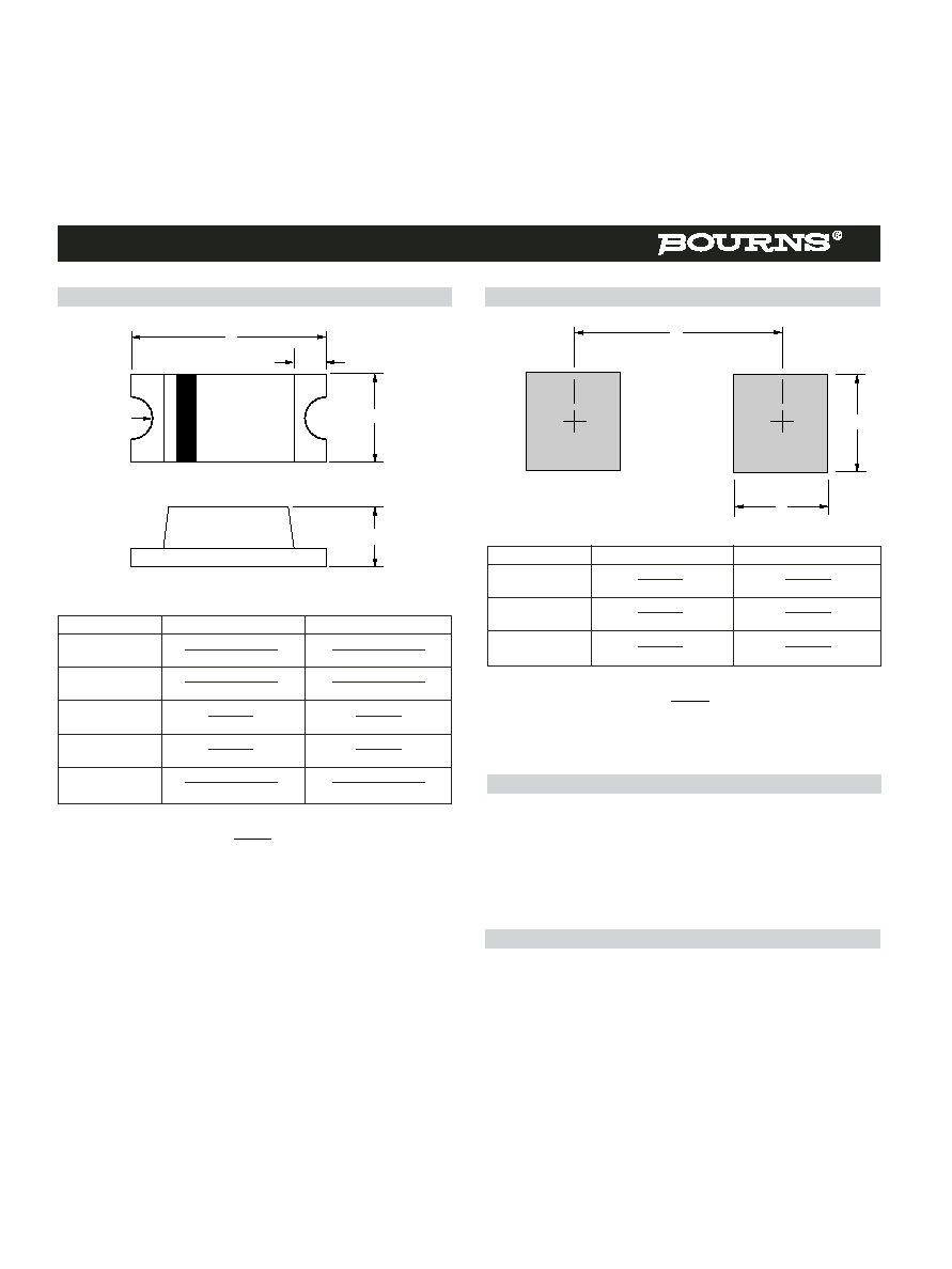
Dimension
0805
1206
A
2.00 - 2.20
3.00 - 3.20
(0.079 - 0.087)
(0.118 - 0.126)
B
1.20 - 1.40
1.40 - 1.60
(0.047 - 0.055)
(0.055 - 0.063)
C
0.40
Typ.
0.50
Typ.
(0.016)
(0.020)
D
0.20
R Typ.
0.25
R Typ.
(0.008)
(0.010)
E
0.90 - 1.10
0.90 - 1.10
(0.035 - 0.043)
(0.035 - 0.043)
Product Dimensions
Recommended Pad Layout
Physical Specifications
Typical Part Marking
Case ....................................0805(2012) / 1206(3216) Molded plastic
Terminals ......................Solder plated, solderable per MIL-STD-750,
Method 2026
Polarity ....................................................Indicated by cathode band
Mounting Position ........................................................................Any
CDxxxx-S0180 ................................................................................S1
CDxxxx-S01575 ..............................................................................S3
CDxxxx-S0180R ..............................................................................S2
A
B
E
C
D
A
C
B
MM
(INCHES)
DIMENSIONS:
Dimension
0805
1206
A (Max.)
2.10
3.00
(0.082)
(0.118)
B (Min.)
1.20
1.60
(0.047)
(0.063)
C (Min.)
1.20
1.40
(0.047)
(0.055)
MM
(INCHES)
DIMENSIONS:

Specifications are subject to change without notice.
Customers should verify actual device performance in their specific applications.
Switching Chip Diode Series - 0805 / 1206
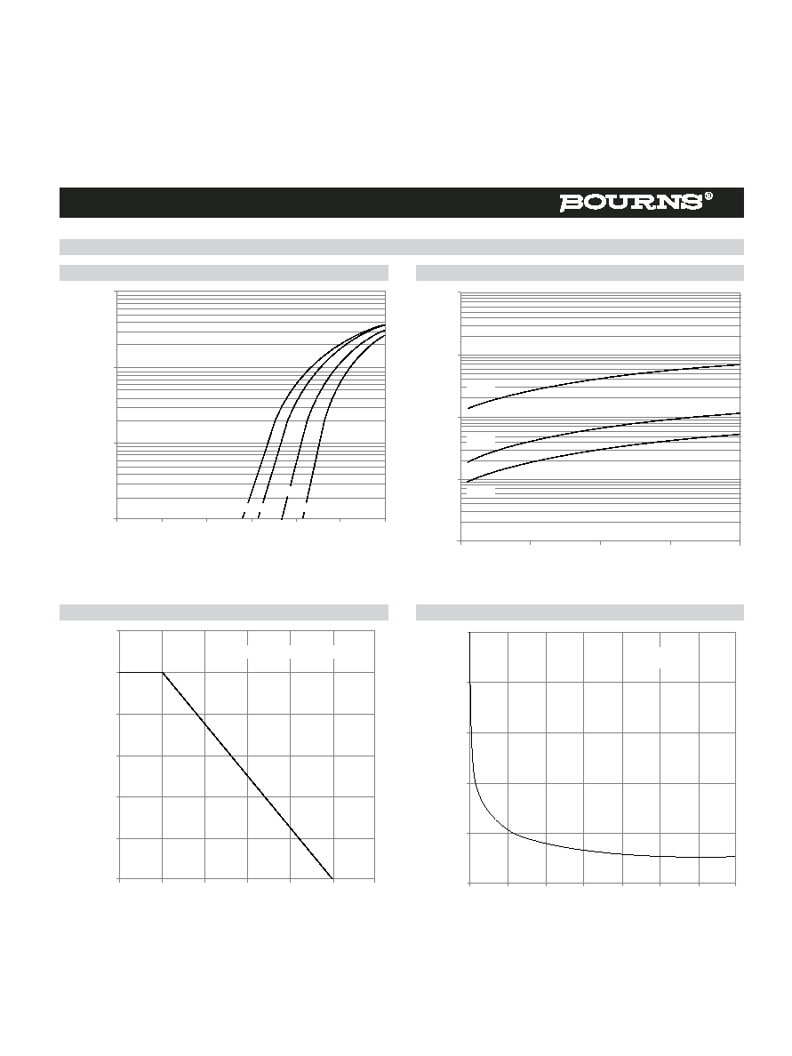
Rating and Characteristic Curves: CDxxxx-S0180
Derating Curve
Capacitance Between Terminals
Forward Characteristics
Reverse Characteristics
1000
100
10
1
For
ward Current (mAmps)
0.0
0.2
0.4
0.6
0.8
1.0
1.2
Forward Voltage (Volts)
125 ∞C 85 ∞C
-25 ∞C
25 ∞C
0
0.1
1
10
100
Reverse Current (nA)
0
10
20
30
40
50
60
70
80
Reverse Voltage (Volts)
25 ∞C
85 ∞C
125 ∞C
120
100
80
60
40
20
0
0
25
50
75
100
125
150
I 0
Current (%)
Ambient Temperature (∞C)
Mounting on glass epoxy PCBs
5.0
4.0
3.0
2.0
1.0
0.0
0
2
4
6
8
10
12
14
Capacitance Between T
erminals (pF)
Reverse Voltage (Volts)
F = 100 MHz
Ta = 25 ∞ C

Specifications are subject to change without notice.
Customers should verify actual device performance in their specific applications.
Switching Chip Diode Series - 0805 / 1206
Rating and Characteristic Curves: CDxxxx-S01575
Derating Curve
Capacitance Between Terminals
Forward Characteristics
Reverse Characteristics
1000
100
1
For
ward Current (mAmps)
0.0
0.2
0.4
0.6
0.8
1.0
1.2
Forward Voltage (Volts)
10
125 ∞C 85 ∞C
-25 ∞C
25 ∞C
0
0.1
Reverse Current (nA)
1.0
10.0
100.0
0
10
20
30
40
50
60
70
80
Reverse Voltage (Volts)
25 ∞C
85 ∞C
125 ∞C
120
100
80
60
40
20
0
0
25
50
75
100
125
150
I 0
Current (%)
Ambient Temperature (∞C)
Mounting on glass epoxy PCBs
5.0
4.0
3.0
2.0
1.0
0.0
0
2
4
6
8
10
12
14
Capacitance Between T
erminals (pF)
Reverse Voltage (Volts)
F = 100 MHz
Ta = 25 ∞C
Specifications are subject to change without notice.
Customers should verify actual device performance in their specific applications.
Switching Chip Diode Series - 0805 / 1206
Rating and Characteristic Curves: CDxxxx-S0180R
Derating Curve
Capacitance Between Terminals
Forward Characteristics
Reverse Characteristics
1000
100
1
For
ward Current (mAmps)
0.0
0.2
0.4
0.6
0.8
1.0
1.2
Forward Voltage (Volts)
10
125 ∞C 85 ∞C
-25 ∞C
25 ∞C
0
0.1
Reverse Current (nA)
1.0
10.0
100.0
0
20
40
60
80
Reverse Voltage (Volts)
25 ∞C
85 ∞C
125 ∞C
120
100
80
60
40
20
0
0
25
50
75
100
125
150
I 0
Current (%)
Ambient Temperature (∞C)
Mounting on glass epoxy PCBs
5.0
4.0
3.0
2.0
1.0
0.0
0
2
4
6
8
10
12
14
Capacitance Between T
erminals (pF)
Reverse Voltage (Volts)
F = 100 MHz
Ta = 25 ∞C