CD214A-B320 ~ B360 Schottky Barrier Rectifier Chip Diode
Specifications are subject to change without notice.
Customers should verify actual device performance in their specific applications.
Features
Lead free versions available
RoHS compliant (lead free version)*
SMA package
Surface mount
High current capability
General Information
The markets of portable communications, computing and video equipment are challenging the semiconductor industry to develop increasingly
smaller electronic components.
Bourns offers Schottky Rectifier Diodes for rectification applications, in compact chip package DO-214AC (SMA) size format, which offer PCB
real estate savings and are considerably smaller than competitive parts. The Schottky Rectifier Diodes offer a forward current of 3 A with a
choice of repetitive peak reverse voltage of 20 V up to 60 V.
Bourns
Æ
Chip Diodes conform to JEDEC standards, easy to handle on standard pick and place equipment and their flat configuration makes
roll away much more difficult.
Parameter
Symbol
CD214A-
Unit
B320
B330
B340
B340L
B350
B360
Forward Voltage (Max.)
VF
0.5
0.5
0.5
0.45
0.7
0.7
V
(If = 3 A)
Typical Junction
CT
250
250
250
300
250
250
pF
Capacitance*
Reverse Current (Max.)
IR
0.5
0.5
0.5
1.0
0.5
0.5
mA
at Rated VR)
Electrical Characteristics (@ TA = 25 ∞C Unless Otherwise Noted)
How To Order
CD 214A - B 3 30 L __
Common Code
Chip Diode
Package
∑ 214A = SMA/DO-214AC
Model
B = Schottky Barrier Series
Average Forward Current (Io) Code
3 = 3 A (Code x 1000 mA = Average Forward Current)
Reverse Voltage (VR) Code
30 = 30 V
40 = 40 V
60 = 60 V
Forward Voltage Suffix
L = Low Forward Voltage Vf (CD214-B330L)
Terminations
LF = 100 % Sn (lead free)
Blank = Sn/Pb
Reliable Electronic Solutions
Asia-Pacific:
Tel: +886-2 2562-4117 ∑ Fax: +886-2 2562-4116
Europe:
Tel: +41-41 768 5555 ∑ Fax: +41-41 768 5510
The Americas:
Tel: +1-951 781-5500 ∑ Fax: +1-951 781-5700
www.bourns.com
Absolute Ratings (@ TA = 25 ∞C Unless Otherwise Noted)
Parameter
Symbol
CD214A-
Unit
B320
B330
B340
B340L
B350
B360
Repetitive Peak
VRRM
20
30
40
40
50
60
V
Reverse Voltage
Reverse Voltage
VR
20
30
40
40
50
60
V
Maximum RMS Voltage
VRMS
14
21
28
28
35
42
V
Avg. Forward Current
IO
3
A
Forward Current,
Surge Peak
Isurge
100
100
100
70
100
100
A
(60 Hz, 1 cycle)
Typical Thermal
RJL
10
10
10
20
10
10
∞C/W
Resistance**
Storage Temperature
TSTG
-55 to +150
∞C
Junction Temperature
TJ
-55 to +125
∞C
* Measured at 1.0 MHz and applied reverse voltage of 4.0 V DC.
** Thermal resistance junction to lead.
*RoHS COMPLIANT
VERSIONS
AVAILABLE
*RoHS Directive 2002/95/EC Jan 27 2003 including Annex
Specifications are subject to change without notice.
Customers should verify actual device performance in their specific applications.
CD214A-B320 ......................................................................
320
CD214A-B330 ......................................................................
330
CD214A-B340 ......................................................................
340
CD214A-B340L ....................................................................
340L
CD214A-B350 ......................................................................
350
CD214A-B360 ......................................................................
360
CD214A-B320 ~ B360 Schottky Barrier Rectifier Chip Diode
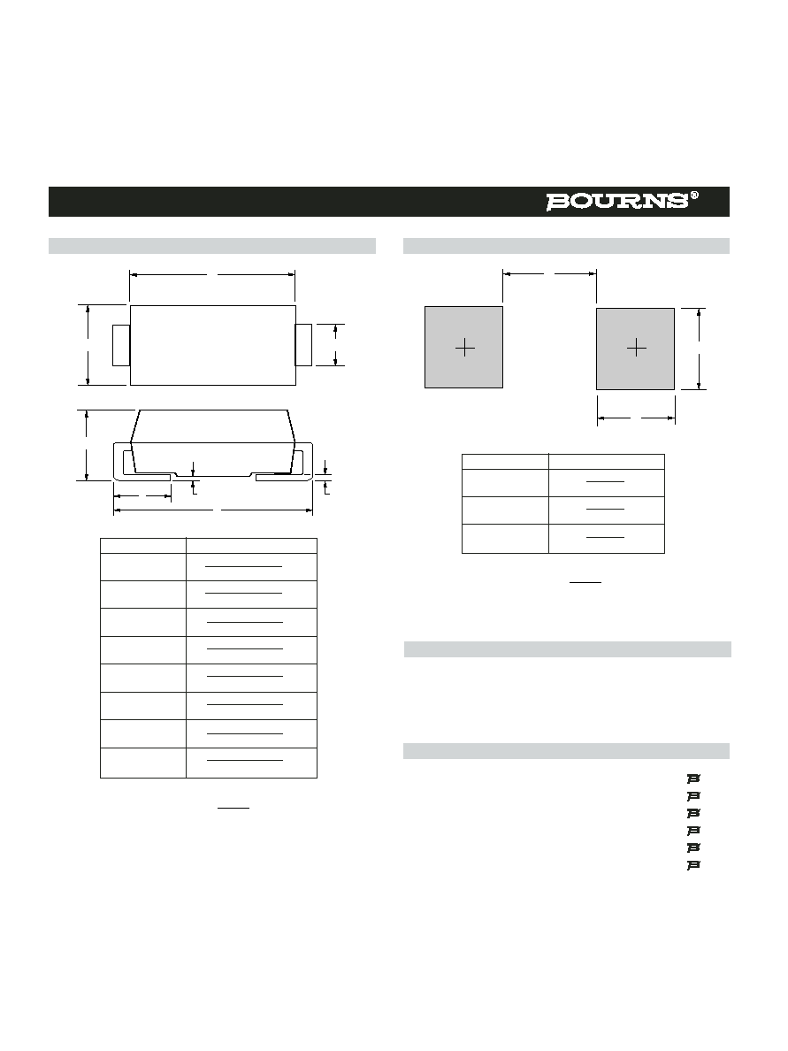
Product Dimensions
Recommended Pad Layout
Physical Specifications
Typical Part Marking
Case ............................................................................Molded plastic
Polarity ....................................................Indicated by cathode band
Weight ....................................................0.002 ounces / 0.064 grams
Dimension
SMA (DO-214AC)
A
4.06 - 4.57
(0.160 - 0.180)
B
2.29 - 2.92
(0.090 - 0.115)
C
1.27 - 1.63
(0.050 - 0.064)
D
0.15 - 0.31
(0.006 - 0.110)
E
4.83 - 5.59
(0.190 - 0.220)
F
0.05 - 0.20
(0.002 - 0.008)
G
2.01 - 2.62
(0.080 - 0.103)
H
0.76 - 1.52
(0.030 - 0.060)
B
G
F
D
C
H
E
A
A
C
B
MM
(INCHES)
DIMENSIONS:
Dimension
SMA (DO-214AC)
A (Max.)
2.69
(0.106)
B (Min.)
2.10
(0.083)
C (Min.)
1.27
(0.050)
MM
(INCHES)
DIMENSIONS:
Specifications are subject to change without notice.
Customers should verify actual device performance in their specific applications.
CD214A-B320 ~ B360 Schottky Barrier Rectifier Chip Diode
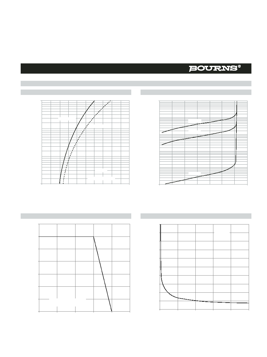
Rating and Characteristic Curves: CD214A-B320, CD214A-B330, CD214A-B340, CD214A-B350 & CD214A-B360
Derating Curve
Capacitance Between Terminals
Forward Characteristics
Reverse Characteristics
0.1
1
10
0.01
Forward Current (Amps)
0.0
0.2
0.4
0.6
0.8
1.0
Forward Voltage (Volts)
Tj=25 ∞C
PULSEWIDTH 300µs
B320 to B340
B350 to B360
100
0.1
1
10
0.001
0.01
Reverse Current (mAmps)
0
20
40
60
80
100
140
Percent of Rated Peak Reverse Voltage (%)
120
Tj=25 ∞C
Tj=100 ∞C
Tj=125 ∞C
3.50
2.50
2.00
3.00
1.50
1.00
0.50
0.00
25
50
75
100
125
150
A
verage For
ward Current (Amps)
Lead Temperature (∞C)
Single Phase Half Wave 60 Hz
Resistive or Inductive Load
1000
100
200
300
400
500
600
700
800
900
0
0
20
40
60
80
100
Capacitance (pF)
Reverse Voltage (Volts)
F = 1 MHz
Ta = 25 ∞C

Specifications are subject to change without notice.
Customers should verify actual device performance in their specific applications.
CD214A-B320 ~ B360 Schottky Barrier Rectifier Chip Diode
Rating and Characteristic Curves: CD214A-B340L
Derating Curve
Capacitance Between Terminals
Forward Characteristics
Reverse Characteristics
0.1
1
10
Forward Current (Amps)
0
0.05 0.10
0.15 0.20
0.25
0.30 0.35 0.40
0.45
0.50
0.55
Forward Voltage (Volts)
Tj=25 ∞C
Tj=100 ∞C
Tj=125 ∞C
PULSEWIDTH 300µs
55
1000
100
0.1
1
10
0.01
Reverse Current (mAmps)
0
5
10
15
20
25
35
40
45
Rated Peak Reverse Voltage (V)
30
Tj=25 ∞C
Tj=100 ∞C
Tj=125 ∞C
3.50
2.50
2.00
3.00
1.50
1.00
0.50
0.00
25
50
75
100
125
150
A
verage For
ward Current (Amps)
Lead Temperature (∞C)
Single Phase Half Wave 60 Hz
Resistive or Inductive Load
1000
100
200
300
400
500
600
700
800
900
0
0
20
40
60
80
100
Capacitance (pF)
Reverse Voltage (Volts)
F = 1 MHz
Ta = 25 ∞C

Specifications are subject to change without notice.
Customers should verify actual device performance in their specific applications.
CD214A-B320 ~ B360 Schottky Barrier Rectifier Chip Diode
Packaging Information
The product will be dispensed in Tape and Reel format (see diagram below).
.......
.......
....... .......
.......
.......
.......
.......
P
A
F
E
T
120 ∞
D2
D
D
1
W1
C
Index Hole
P
0
P
1
W
B
10 pitches (min.)
Direction of Feed
10 pitches (min.)
End
Trailer
Device
Leader
Start
d
Devices are packed in accordance with EIA standard
RS-481-A and specifications shown here.
MM
(INCHES)
DIMENSIONS:
Item
Symbol
SMA (DO-214AC)
Carrier Width
A
2.90 ± 0.10
(0.114 - 0.004)
Carrier Length
B
5.59 ± 0.10
(0.220 - 0.004)
Carrier Depth
C
2.36 ± 0.10
(0.093 - 0.004)
Sprocket Hole
d
1.55 ± 0.05
(0.061 - 0.002)
Reel Outside Diameter
D
330
(12.992)
Reel Inner Diameter
D1
50.0
MIN.
(1.969)
Feed Hole Diameter
D2
13.0 ± 0.20
(0.512 - 0.008)
Sprocket Hole Position
E
1.75 ± 0.10
(0.069 - 0.004))
Punch Hole Position
F
5.50 ± 0.05
(0.217 - 0.002)
Punch Hole Pitch
P
4.00 ± 0.10
(0.157 - 0.004)
Sprocket Hole Pitch
P0
4.00 ± 0.10
(0.157 - 0.004)
Embossment Center
P1
2.00 ± 0.05
(0.079 - 0.002)
Overall Tape Thickness
T
0.30 ± 0.10
(0.012 - 0.004)
Tape Width
W
12.00 ± 0.20
(0.472 - 0.008)
Reel Width
W1
18.4
MAX.
(0.724)
Quantity per Reel
--
5,000
REV. 02/05