 | –≠–ª–µ–∫—Ç—Ä–æ–Ω–Ω—ã–π –∫–æ–º–ø–æ–Ω–µ–Ω—Ç: ADS1254 | –°–∫–∞—á–∞—Ç—å:  PDF PDF  ZIP ZIP |
24-Bit, 20kHz, Low Power
ANALOG-TO-DIGITAL CONVERTER
FEATURES
q
24 BITS--NO MISSING CODES
q
19 BITS EFFECTIVE RESOLUTION UP TO
20kHz DATA RATE
q
LOW NOISE: 1.8ppm
q
FOUR DIFFERENTIAL INPUTS
q
INL: 15ppm (max)
q
EXTERNAL REFERENCE (0.5V to 5V)
q
POWER-DOWN MODE
q
SYNC MODE
q
LOW POWER: 4mW at 20kHz
q
SEPARATE DIGITAL INTERFACE SUPPLY 1.8V
to 3.6V
DESCRIPTION
The ADS1254 is a precision, wide dynamic range, delta-
sigma, Analog-to-Digital (A/D) converter with 24-bit reso-
lution. The delta-sigma architecture is used for wide dy-
namic range and to ensure 24 bits of no missing codes
performance. An effective resolution of 19 bits (1.8ppm of
rms noise) is achieved for conversion rates up to 20kHz.
The ADS1254 is designed for high-resolution measurement
applications in cardiac diagnostics, smart transmitters, in-
dustrial process control, weight scales, chromatography, and
portable instrumentation. The converter includes a flexible,
two-wire synchronous serial interface for low-cost isolation.
The ADS1254 is a multi-channel converter and is offered in
an SSOP-20 package.
APPLICATIONS
q
CARDIAC DIAGNOSTICS
q
DIRECT THERMOCOUPLE INTERFACES
q
BLOOD ANALYSIS
q
INFRARED PYROMETERS
q
LIQUID/GAS CHROMATOGRAPHY
q
PRECISION PROCESS CONTROL
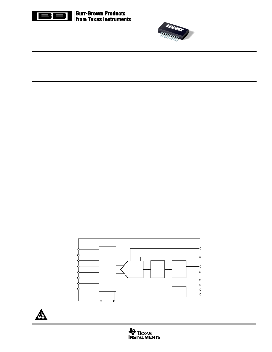
ADS1254
SBAS213 ≠ JUNE 2001
4th-Order
Modulator
Digital
Filter
Serial
Interface
Control
CLK
V
REF
SCLK
DOUT/DRDY
AV
DD
DV
DD
AGND
DGND
ADS1254
Mux
CH1+
CH1≠
CH2+
CH2≠
CH3+
CH3≠
CH4+
CH4≠
CHSEL0
CHSEL1
www.ti.com
PRODUCTION DATA information is current as of publication date.
Products conform to specifications per the terms of Texas Instruments
standard warranty. Production processing does not necessarily include
testing of all parameters.
Copyright © 2001, Texas Instruments Incorporated
Please be aware that an important notice concerning availability, standard warranty, and use in critical applications of
Texas Instruments semiconductor products and disclaimers thereto appears at the end of this data sheet.
ADS1254

ADS1254
2
SBAS213
Analog Input: Current (Momentary) ..............................................
±
100mA
(Continuous) ...............................................
±
10mA
Voltage ................................... GND ≠ 0.3V to V
DD
+ 0.3V
AV
DD
to AGND ....................................................................... ≠0.3V to 6V
DV
DD
to AV
DD
.......................................................................... ≠6V to +6V
DV
DD
to DGND ....................................................................... ≠0.3V to 6V
V
REF
Voltage to AGND ............................................. ≠0.3V to V
DD
+ 0.3V
Digital Input Voltage to DGND ................................. ≠0.3V to V
DD
+ 0.3V
Digital Output Voltage to DGND .............................. ≠0.3V to V
DD
+ 0.3V
Lead Temperature (soldering, 10s) .............................................. +300
∞
C
Power Dissipation (any package) ................................................. 500mW
ABSOLUTE MAXIMUM RATINGS
PACKAGE
SPECIFIED
DRAWING
TEMPERATURE
PACKAGE
ORDERING
TRANSPORT
PRODUCT
PACKAGE
NUMBER
RANGE
MARKING
NUMBER
(1)
MEDIA
ADS1254E
SSOP-20
349
≠40
∞
C to +85
∞
C
ADS1254E
ADS1254E
Rails
"
"
"
"
"
ADS1254E/2K5
Tape and Reel
NOTE: (1) Models with a slash (/) are available only in Tape and Reel in the quantities indicated (e.g., /2K5 indicates 2500 devices per reel). Ordering 2500 pieces
of "ADS1254E/2K5" will get a single 2500-piece Tape and Reel.
PACKAGE/ORDERING INFORMATION
ELECTROSTATIC
DISCHARGE SENSITIVITY
This integrated circuit can be damaged by ESD. Texas Instru-
ments recommends that all integrated circuits be handled with
appropriate precautions. Failure to observe proper handling
and installation procedures can cause damage.
ESD damage can range from subtle performance degradation
to complete device failure. Precision integrated circuits may
be more susceptible to damage because very small parametric
changes could cause the device not to meet its published
specifications.
ANALOG INPUT
Input Voltage Range
AGND
±
V
REF
V
Input Impedance
CLK = 3,840Hz
260
M
CLK = 1MHz
1
M
CLK = 8MHz
125
k
Input Capacitance
6
pF
Input Leakage
At +25
∞
C
5
50
pA
At T
MIN
to T
MAX
1
nA
DYNAMIC CHARACTERISTICS
Data Rate
20.8
kHz
Bandwidth
≠3dB
4.24
kHz
Serial Clock (SCLK)
8
MHz
System Clock Input (CLK)
8
MHz
ACCURACY
Integral Non-Linearity
(1)
±
0.0002
±
0.0015
% of FSR
THD
1kHz Input; 0.1dB below FS
105
dB
Noise
1.8
2.7
ppm of FSR, rms
Resolution
24
Bits
No Missing Codes
24
Bits
Common-Mode Rejection
60Hz, AC
90
102
dB
Gain Error
0.1
1
% of FSR
Offset Error
±
30
±
100
ppm of FSR
Gain Sensitivity to V
REF
1:1
Power-Supply Rejection Ratio
70
88
dB
PERFORMANCE OVER TEMPERATURE
Offset Drift
0.07
ppm/
∞
C
Gain Drift
0.4
ppm/
∞
C
VOLTAGE REFERENCE
V
REF
0.5
4.096
V
DD
V
Load Current
32
µ
A
ADS1254E
PARAMETER
CONDITIONS
MIN
TYP
MAX
UNITS
ELECTRICAL CHARACTERISTICS
All specifications at T
MIN
to T
MAX
, AV
DD
= +5V, DV
DD
= +1.8V. CLK = 8MHz, and V
REF
= 4.096, unless otherwise specified.
NOTE: (1) Applies to full-differential signals.
ADS1254
3
SBAS213
ELECTRICAL CHARACTERISTICS
(Cont.)
All specifications at T
MIN
to T
MAX
, AV
DD
= +5V, DV
DD
= +1.8V. CLK = 8MHz, and V
REF
= 4.096, unless otherwise specified.
ADS1254E
PARAMETER
CONDITIONS
MIN
TYP
MAX
UNITS
DIGITAL INPUT/OUTPUT
Logic Family
CMOS
Logic Level: V
IH
0.65 ∑ DV
DD
DV
DD
+ 0.3
V
V
IL
≠0.3
0.35 ∑ DV
DD
V
V
OH
I
OH
= ≠500
µ
A
DV
DD
≠0.4
V
V
OL
I
OL
= 500
µ
A
0.4
V
Input (SCLK, CLK, CHSEL0, CHSEL1) Hysteresis
0.6
V
Data Format
Offset Binary Two's Complement
POWER-SUPPLY REQUIREMENTS
Power Supply Voltage
DV
DD
1.8
3.6
VDC
AV
DD
4.75
5
5.25
VDC
Quiescent Current
AV
DD
= +5V
0.8
1.15
mA
DV
DD
= +1.8V
0.2
0.4
mA
Operating Power
4.3
6.5
mW
Power-Down Current
0.4
1
µ
A
TEMPERATURE RANGE
Operating
≠40
+85
∞
C
Storage
≠60
+100
∞
C
CH1+
ADS1254E
CH4≠
CH1≠
CH4+
CH2+
V
REF
AGND
CH2≠
1
2
3
4
20
19
18
17
16
15
14
13
12
11
CH3+
CHSEL1
CH3≠
CHSEL0
AV
DD
SCLK
DOUT/DRDY
CLK
5
6
7
8
9
10
DV
DD
DGND
NC
NC
PIN CONFIGURATION
Top View
SSOP-20
PIN DESCRIPTIONS
PIN
NAME
PIN DESCRIPTION
1
CH1+
Analog Input: Positive Input of the Differen-
tial Analog Input
2
CH1≠
Analog Input: Negative Input of the Differ-
ential Analog Input
3
CH2+
Analog Input: Positive Input of the Differen-
tial Analog Input
4
CH2≠
Analog Input: Negative Input of the Differ-
ential Analog Input
5
CH3+
Analog Input: Positive Input of the Differen-
tial Analog Input
6
CH3≠
Analog Input: Negative Input of the Differ-
ential Analog Input
7
AV
DD
Input: Analog Power Supply Voltage, +5V
8
CLK
Digital Input: Device System Clock. The
system clock is in the form of a CMOS-
compatible clock. This is a Schmitt-Trigger
input
9
DV
DD
Input: Digital Power Supply Voltage
10
NC
No Connection
11
NC
No Connection
12
DGND
Input: Digital Ground
13
DOUT/DRDY
Digital Output: Serial Data Output/Data
Ready. This output indicates that a new
output word is available from the ADS1254
data output register. The serial data is
clocked out of the serial data output shift
register using SCLK.
14
SCLK
Digital Input: Serial Clock. The serial clock
is in the form of a CMOS-compatible clock.
The serial clock operates independently
from the system clock, therefore, it is pos-
sible to run SCLK at a higher frequency
than CLK. The normal state of SCLK is
LOW. Holding SCLK HIGH will either ini-
tiate a modulator reset for synchronizing
multiple converters or enter power-down
mode. This is a Schmitt-Trigger input.
15
CHSEL1
Digital Input: Used to select analog input
channel. This is a Schmitt-Trigger Input
16
CHSEL0
Digital Input: Used to select analog input
channel. This is a Schmitt-Trigger Input
17
AGND
Input: Analog Ground
18
V
REF
Analog Input: Reference Voltage Input
19
CH4≠
Analog Input: Negative Input of the Differ-
ential Analog Input
20
CH4+
Analog Input: Positive Input of the Differen-
tial Analog Input
ADS1254
4
SBAS213
TYPICAL CHARACTERISTICS
At T
A
= +25
∞
C, AV
DD
= +5V, DV
DD
= +1.8V, CLK = 8MHz, and V
REF
= 4.096, unless otherwise specified.
2.0
1.8
1.6
1.4
1.2
1.0
0.8
0.6
0.4
0.2
0.0
RMS NOISE vs TEMPERATURE
Temperature (
∞
C)
≠40
≠20
0
20
40
60
80
100
RMS Noise (ppm of FS)
20
19.8
19.6
19.4
19.2
19.0
18.8
18.6
18.4
18.2
18.0
EFFECTIVE RESOLUTION vs TEMPERATURE
Temperature (
∞
C)
≠40
≠20
0
20
40
60
80
100
Effective Resolution (Bits)
10
9
8
7
6
5
4
3
2
1
0
V
REF
Voltage (V)
0.5
1.0
1.5
2.0
2.5
3.0
3.5
4.0
4.5
5.0
RMS Noise (
µ
V)
RMS NOISE vs V
REF
Voltage
12
10
8
6
4
2
0
V
REF
Voltage (V)
0.5
1.0
1.5
2.0
2.5
3.0
3.5
4.0
4.5
5
RMS Noise (ppm of FS)
RMS NOISE vs V
REF
Voltage
2.0
1.9
1.8
1.7
1.6
1.5
1.4
1.3
1.2
1.1
1.0
RMS Noise (ppm of FS)
RMS NOISE vs DATA OUTPUT RATE
100
1k
10k
100k
Data Ouput Rate (Hz)
20.0
19.8
19.6
19.4
19.2
19.0
18.8
18.6
18.4
18.2
18.0
Ef
fective Resolution (Bits)
EFFECTIVE RESOLUTION vs DATA OUTPUT RATE
100
1k
10k
100k
Data Ouput Rate (Hz)
ADS1254
5
SBAS213
TYPICAL CHARACTERISTICS
(Cont.)
At T
A
= +25
∞
C, AV
DD
= +5V, DV
DD
= +1.8V, CLK = 8MHz, and V
REF
= 4.096, unless otherwise specified.
2
1.5
1
0.5
0
Input Voltage (V)
≠5
≠4
≠3
≠2
≠1
0
1
2
3
4
5
RMS Noise (ppm of FS)
RMS NOISE vs INPUT VOLTAGE
2.5
2.0
1.5
1.0
0.5
0
INTEGRAL NONLINEARITY vs TEMPERATURE
Temperature (
∞
C)
≠40
≠20
0
20
40
60
80
100
INL (ppm of FS)
600
580
560
540
520
500
480
GAIN ERROR vs TEMPERATURE
Temperature (
∞
C)
≠60
≠40
≠20
0
20
40
60
80
100
Gain Error (ppm of FS)
≠0
≠10
≠20
≠30
≠40
≠50
≠60
≠70
≠80
≠90
≠100
PSR vs CLK FREQUENCY
Clock Frequency (MHz)
1
2
3
4
5
6
7
8
PSR (dB)
20
18
16
14
12
10
8
6
4
2
0
OFFSET vs TEMPERATURE
Temperature (
∞
C)
≠40
≠20
0
20
40
60
80
100
DC Offset (ppm of FS)
6
5
4
3
2
1
0
INTEGRAL NON-LINEARITY vs DATA OUTPUT RATE
Data Output Rate (Hz)
100
1k
10k
100k
INL (ppm of FS)