 | –≠–ª–µ–∫—Ç—Ä–æ–Ω–Ω—ã–π –∫–æ–º–ø–æ–Ω–µ–Ω—Ç: ADS2806Y | –°–∫–∞—á–∞—Ç—å:  PDF PDF  ZIP ZIP |
Document Outline
- FEATURES
- APPLICATIONS
- DESCRIPTION
- ABSOLUTE MAXIMUM RATINGS
- PACKAGE/ORDERING INFORMATION
- ELECTRICAL CHARACTERISTICS
- TIMING DIAGRAM
- PIN CONFIGURATION
- PIN DESCRIPTIONS
- TYPICAL CHARACTERISTICS
- APPLICATION INFORMATION
- THEORY OF OPERATION
- DRIVING THE ANALOG INPUTS
- AC-Coupled, Single-Ended to Differential Interface with Dual-Supply Op Amps
- Transformer Coupled, Single-Ended to Differential Configuration
- AC-Coupled, Single-Ended-to-Differential Interface for Single-Supply Operation
- Single-Ended, AC-Coupled, Dual-Supply Interface
- DC-Coupled, Differential Driver with Level Shift
- REFERENCE OPERATION
- USING EXTERNAL REFERENCES
- DIGITAL INPUTS AND OUTPUTS
- Clock Input Requirements
- Over Range Indicator (OVR)
- Data Outputs
- Digital Output Driver Supply (VDRV)
- OUTPUT ENABLE (OE)\
- GROUNDING AND DECOUPLING
- PACKAGE DRAWING
- PAP (S-PQFP-G64) PowerPAD . PLASTIC QUAD FLATPACK

ADS2806
Dual, 12-Bit, 32MHz Sampling
ANALOG-TO-DIGITAL CONVERTER
FEATURES
q
SPURIOUS-FREE DYNAMIC RANGE:
73dB at 10MHz f
IN
q
HIGH SNR: 67dB (2Vp-p), 69dB (3Vp-p)
q
INTERNAL OR EXTERNAL REFERENCE
q
LOW DLE:
±
0.4LSB
q
FLEXIBLE INPUT RANGE: 2Vp-p to 3Vp-p
q
TQFP-64 POWER PACKAGE
DESCRIPTION
The ADS2806 is a dual, high-speed, high dynamic range,
12-bit pipelined Analog-to-Digital Converter (ADC). This con-
verter includes a high-bandwidth track-and-hold that gives
excellent spurious performance up to and beyond the Nyquist
rate. The differential nature of this track-and-hold and ADC
circuitry minimizes even-order harmonics and gives excel-
lent common-mode noise immunity. The track-and-hold can
also be operated single-ended.
The ADS2806 provides for setting the full-scale range of the
converter without any external reference circuitry. The internal
APPLICATIONS
q
COMMUNICATIONS IF PROCESSING
q
COMMUNICATIONS BASESTATIONS
q
TEST EQUIPMENT
q
MEDICAL IMAGING
q
VIDEO DIGITIZING
q
CCD DIGITIZING
Optional External
Reference
12-Bit
Pipelined
A/D
Error
Correction
Logic
Timing
Circuitry
Internal
Reference
3-State
Outputs
T&H
D12A
∑
∑
∑
D1A
12-Bit
Pipelined
A/D
Error
Correction
Logic
3-State
Outputs
T&H
D12B
∑
∑
∑
D1B
IN
A
+V
S
OE
A
OVR
A
OVR
B
IN
A
INT/EXT
CLK
FS
SEL
(Opt.)
IN
B
V
IN
CM
OE
B
IN
B
(Opt.)
ADS2806
V
IN
reference can be disabled allowing low drive, external refer-
ences to be used for improved tracking in multichannel systems.
The ADS2806 provides an over-range indicator flag to
indicate an input signal that exceeds the full-scale input
range of the converter. This flag can be used to reduce the
gain of front end gain control circuitry. There is also an
output enable pin to allow for multiplexing and testability on
a PC board.
The ADS2806 employs digital error correction techniques to
provide excellent differential linearity for demanding imag-
ing applications. The ADS2806 is available in a TQFP-64
power package.
ADS2806
SBAS178B ≠ DECEMBER 2000 ≠ REVISED MAY 2002
www.ti.com
PRODUCTION DATA information is current as of publication date.
Products conform to specifications per the terms of Texas Instruments
standard warranty. Production processing does not necessarily include
testing of all parameters.
Copyright © 2000, Texas Instruments Incorporated
Please be aware that an important notice concerning availability, standard warranty, and use in critical applications of
Texas Instruments semiconductor products and disclaimers thereto appears at the end of this data sheet.
ADS2806
SBAS178B
2
www.ti.com
ADS2806Y
PARAMETER
CONDITIONS
MIN
TYP
MAX
UNITS
RESOLUTION
12 Tested
Bits
SPECIFIED TEMPERATURE RANGE
Ambient Air
≠40
+85
∞
C
ANALOG INPUT
2V Full-Scale Input Range (Differential)
2Vp-p, INT or EXT Ref
2
3
V
2V Full-Scale Input Range (Single-Ended)
2Vp-p, INT or EXT Ref
1.5
3.5
V
3V Full-Scale Input Range (Differential)
3Vp-p, INT or EXT Ref
1.75
3.25
V
3V Full-Scale Input Range (Single-Ended)
3Vp-p, INT or EXT Ref
1
4
V
Analog Input Bias Current
1
µ
A
Analog Input Bandwidth
270
MHz
Input Impedance
1.25 || 3
M
|| pF
CONVERSION CHARACTERISTICS
Sample Rate
10k
32
Samples/s
Data Latency
6
Clock Cycles
DYNAMIC CHARACTERISTICS
Differential Linearity Error (largest code error)
f = 1MHz
±
0.35
±
1.0
LSB
f = 10MHz
±
0.4
LSB
No Missing Codes
Tested
Integral Linearity Error, f = 1MHz
±
2.5
±
4.0
LSBs
Spurious-Free Dynamic Range
(1)
f = 1MHz (≠1dB input)
73
dBFS
(2)
f = 10MHz (≠1dB input)
67
73
dBFS
2-Tone Intermodulation Distortion
(3)
f = 9MHz and 10MHz (≠7dB each tone)
≠74.6
dBc
Signal-to-Noise Ratio (SNR)
f = 1MHz (≠1dB input)
67
dBFS
f = 10MHz (≠1dB input)
63
66
dBFS
f = 1MHz (≠1dB input)
3Vp-p
69
dBFS
f = 10MHz (≠1dB input)
3Vp-p
68
dBFS
Signal-to-(Noise + Distortion) (SINAD)
(4)
f = 1MHz (≠1dBFS input)
66
dBFS
f = 10MHz (≠1dBFS input)
61
65
dBFS
f = 1MHz (≠1dBFS input)
3Vp-p
69
dBFS
f = 10MHz (≠1dBFS Input)
3Vp-p
69
dBFS
ELECTRICAL CHARACTERISTICS
At T
A
= full specified temperature range, V
S
= +5V, differential input range = 2V to 3V for each input, sampling rate = 32MSPS, unless otherwise noted.
+V
S
....................................................................................................... +6V
Analog Input ........................................................... (≠0.3V) to (+V
S
+ 0.3V)
Logic Input ............................................................. (≠0.3V) to (+V
S
+ 0.3V)
Case Temperature ......................................................................... +100
∞
C
Junction Temperature .................................................................... +150
∞
C
Storage Temperature ..................................................................... +150
∞
C
NOTE: (1) Stresses above those listed under "Absolute Maximum Ratings"
may cause permanent damage to the device. Exposure to absolute maximum
conditions for extended periods may affect device reliability.
ABSOLUTE MAXIMUM RATINGS
(1)
ELECTROSTATIC
DISCHARGE SENSITIVITY
This integrated circuit can be damaged by ESD. Texas Instru-
ments recommends that all integrated circuits be handled with
appropriate precautions. Failure to observe proper handling
and installation procedures can cause damage.
ESD damage can range from subtle performance degradation
to complete device failure. Precision integrated circuits may be
more susceptible to damage because very small parametric
changes could cause the device not to meet its published
specifications.
SPECIFIED
PACKAGE
TEMPERATURE
PACKAGE
ORDERING
TRANSPORT
PRODUCT
PACKAGE-LEAD
DESIGNATOR
(1)
RANGE
MARKING
NUMBER
MEDIA, QUANTITY
ADS2806Y
TQFP-64
PAP
≠40
∞
C to +85
∞
C
ADS2806Y
ADS2806Y/1K5
Tape and Reel, 1500
"
"
"
"
"
ADS2806Y/250
Tape and Reel, 250
NOTE: (1) For the most current specifications and package information, refer to our web site at www.ti.com.
PACKAGE/ORDERING INFORMATION

ADS2806
SBAS178B
3
www.ti.com
ELECTRICAL CHARACTERISTICS
(Cont.)
At T
A
= full specified temperature range, V
S
= +5V, differential input range = 2V to 3V for each input, sampling rate = 32MSPS, unless otherwise noted.
ADS2806Y
PARAMETER
CONDITIONS
MIN
TYP
MAX
UNITS
DYNAMIC CHARACTERISTICS (Cont.)
Channel-to-Channel Crosstalk
2Vp-p
80
dBc
Output Noise
Input Grounded
0.2
LSBs rms
Aperture Delay Time
2
ns
Aperture Jitter
1.2
ps rms
Overvoltage Recovery Time
2
ns
DIGITAL INPUTS
Logic Family
+3V/+5V CMOS Compatible
Convert Command
Start Conversion
Rising Edge of Convert Clock
High Level Input Current
(5)
(V
IN
= 5V)
+50
µ
A
Low Level Input Current (V
IN
= 0V)
+10
µ
A
High Level Input Voltage
+2.4
V
Low Level Input Voltage
+1.0
V
Input Capacitance
5
pF
DIGITAL OUTPUTS
Logic Family
CMOS
Logic Coding
Straight Offset Binary
Low Output Voltage (I
OL
= 50
µ
A)
VDRV = 5V
+0.1
V
Low Output Voltage, (I
OL
= 1.6mA)
VDRV = 5V
+0.2
V
High Output Voltage, (I
OH
= 50
µ
A)
VDRV = 5V
+4.9
V
High Output Voltage, (I
OH
= 0.5mA)
VDRV = 5V
+4.8
V
Low Output Voltage, (I
OL
= 50
µ
A)
VDRV = 3V
+0.4
V
High Output Voltage, (I
OH
= 50
µ
A)
VDRV = 3V
+2.4
V
3-State Enable Time
OE = L
(5)
20
40
ns
3-State Disable Time
OE = H
(5)
2
10
ns
Output Capacitance
5
pF
ACCURACY (Internal Reference,
2Vp-p, Unless Otherwise Noted)
Zero Error (Midscale)
at 25
∞
C
±
0.5
%FS
Zero Error Drift (Midscale)
16
ppm/
∞
C
Gain Error
(6)
at 25
∞
C
±
1.5
%FS
Gain Error Drift
(6)
66
ppm/
∞
C
Gain Error
(7)
at 25
∞
C
±
1.0
%FS
Gain Error Drift
(7)
23
ppm/
∞
C
Power-Supply Rejection of Gain
V
S
=
±
5%
70
dB
REFT Tolerance
2V Full Scale
Deviation From Ideal 3.0V
±
10
±
65
mV
3V Full Scale
Deviation From Ideal 3.25V
±
20
mV
REFB Tolerance
2V Full Scale
Deviation From Ideal 2.0V
±
10
±
65
mV
3V Full Scale
Deviation From Ideal 1.75V
±
20
mV
External REFT Voltage Range
REFB + 0.4
3
V
S
≠ 1.70
V
External REFB Voltage Range
1.70
2
REFT ≠ 0.4
V
Reference Input Resistance
375
POWER-SUPPLY REQUIREMENTS
Supply Voltage: +V
S
Operating
+4.75
+5.0
+5.25
V
Supply Current: +I
S
Operating
78
mA
Power Dissipation: VDRV = 5V
External Reference
430
mW
VDRV = 3V
External Reference
400
mW
VDRV = 5V
Internal Reference
450
mW
VDRV = 3V
Internal Reference
420
475
mW
Thermal Resistance,
JA
TQFP-64
21.5
∞
C/W
NOTES: (1) Spurious-Free Dynamic Range refers to the magnitude of the largest harmonic. (2) dBFS means dB relative to Full-Scale. (3) 2-tone intermodulation
distortion is referred to the largest fundamental tone. This number will be 6dB higher if it is referred to the magnitude of the 2-tone fundamental envelope.
(4) Effective number of bits (ENOB) is defined by as (SINAD ≠ 1.76) /6.02. (5) A 50k
pull-down resistor is inserted internally on OE pins. (6) Includes internal
reference. (7) Excludes internal reference.
ADS2806
SBAS178B
4
www.ti.com
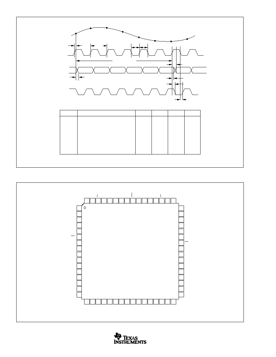
PIN CONFIGURATION
Top View
TQFP
48
47
46
45
44
43
42
41
40
39
38
37
36
35
34
33
GND
GND
+V
S
SEL
GND
+V
S
OE
A
GND
VDRV
A
OVR
A
A1 (MSB)
A2
A3
A4
A5
A6
1
2
3
4
5
6
7
8
9
10
11
12
13
14
15
16
GND
GND
+V
S
GND
+V
S
OE
B
GND
VDRV
B
OVR
B
B12 (LSB)
B11
B10
B9
B8
B7
B6
GND
IN
B
IN
B
CM
B
REFT
B
REFB
B
GND
+V
S
INT/EXT
GND
REFB
A
REFT
A
CM
A
IN
A
IN
A
GND
B5
B4
B3
B2
B1(MSB)
DV
B
GND
CLK
GND
DV
A
A12 (LSB)
A11
A10
A9
A8
A7
64
63
62
61
60
59
58
57
56
55
54
17
18
19
20
21
22
23
24
25
26
27
53
52
51
50
49
28
29
30
31
32
ADS2806Y
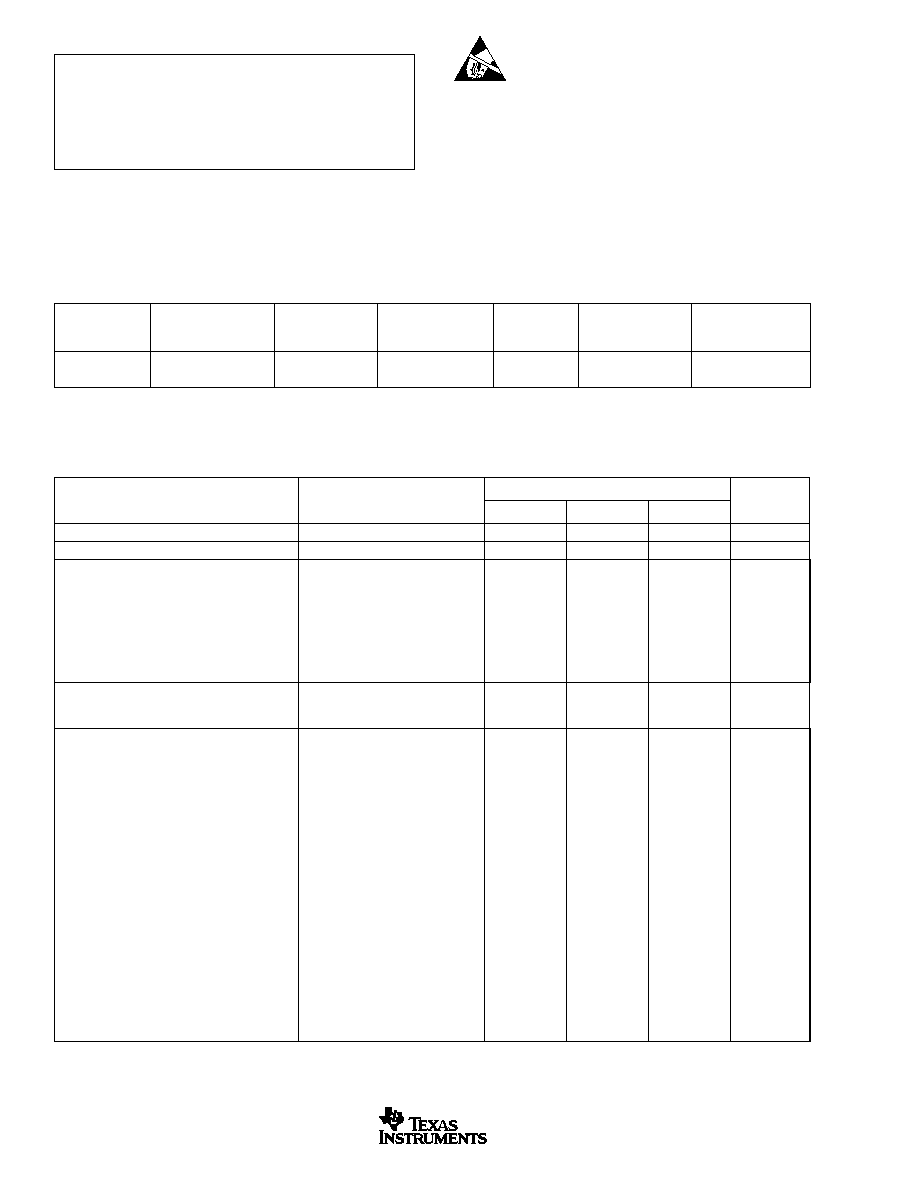
TIMING DIAGRAM
6 Clock Cycles
Data Invalid
t
D
t
L
t
H
t
CONV
N ≠ 6
N ≠ 5
N ≠ 4
N ≠ 3
N ≠ 2
N ≠ 1
N
N + 1
Data Out
Data Valid
Clock
Analog In
N
t
2
N + 1
N + 2
N + 3
N + 4
N + 5
N + 6
N + 7
t
1
t
3
t
4
SYMBOL
DESCRIPTION
MIN
TYP
MAX
UNITS
t
CONV
Convert Clock Period
31.25
100
µ
s
ns
t
L
Clock Pulse Low
14.6
t
CONV
/2
ns
t
H
Clock Pulse High
14.6
t
CONV
/2
ns
t
D
Aperture Delay
2
ns
t
1
(1)
Data Hold Time, C
L
= 0pF
2.7
ns
t
2
(1)
New Data Delay Time, C
L
= 15pF max
8.2
12
ns
t
3
Data Valid Falling Edge Delay, C
L
= 15pF max
7.5
ns
t
4
Data Valid Rising Edge Delay, C
L
= 15pF max
5.6
ns
NOTE: (1) t
1
and t
2
times are valid for VDRV voltages of +2.7V to +5V.
ADS2806
SBAS178B
5
www.ti.com
PIN
I/O
DESIGNATOR
DESCRIPTION
1
GND
Ground
2
GND
Ground
3
+V
S
+5V Supply
4
GND
Ground
5
+V
S
+5V Supply
6
I
OE
B
Output Enable, Channel B
7
GND
GND
8
VDRV
B
Logic Driver Supply Voltage, Channel B
9
O
OVR
B
Over-Range Indicator, Channel B
10
O
B12 (LSB)
Data Bit 12 (D0), Channel B
11
O
B11
Data Bit 11 (D1), Channel B
12
O
B10
Data Bit 10 (D2), Channel B
13
O
B9
Data Bit 9 (D3), Channel B
14
O
B8
Data Bit 8 (D4), Channel B
15
O
B7
Data Bit 7 (D5), Channel B
16
O
B6
Data Bit 6 (D6), Channel B
17
O
B5
Data Bit 5 (D7), Channel B
18
O
B4
Data Bit 4 (D8), Channel B
19
O
B3
Data Bit 3 (D9), Channel B
20
O
B2
Data Bit 2 (D10), Channel B
21
O
B1 (MSB)
Data Bit 1 (D11), Channel B
22
O
DV
B
Data Valid, Channel B
23
GND
Ground
24
I
CLK
Clock
25
GND
Ground
26
O
DV
A
Data Valid, Channel A
27
O
A12 (LSB)
Data Bit 12 (D0), Channel A
28
O
A11
Data Bit 11 (D1), Channel A
29
O
A10
Data Bit 10 (D2), Channel A
30
O
A9
Data Bit 9 (D3), Channel A
31
O
A8
Data Bit 8 (D4), Channel A
32
O
A7
Data Bit 7 (D5), Channel A
33
O
A6
Data Bit 6 (D6), Channel A
PIN DESCRIPTIONS
PIN
I/O
DESIGNATOR
DESCRIPTION
34
O
A5
Data Bit 5 (D7), Channel A
35
O
A4
Data Bit 4 (D8), Channel A
36
O
A3
Data Bit 3 (D9), Channel A
37
O
A2
Data Bit 2 (D10), Channel A
38
O
A1 (MSB)
Data Bit 1 (D11), Channel A
39
O
OVR
A
Over-Range Indicator, Channel A
40
VDRV
A
Logic Driver Supply Voltage, Channel A
41
GND
Ground
42
I
OE
A
Output Enable, Channel A
43
+V
S
+5V Supply
44
GND
Ground
45
I
SEL
Input Range Select: HIGH = 3V, LOW = 2V
46
+V
S
+5V Supply
47
GND
Ground
48
GND
Ground
49
GND
Ground
50
I
IN
A
Analog Input, Channel A
51
I
IN
A
Complementary Analog Input, Channel A
52
O
CM
A
Common-Mode, Channel A
53
I/O
REFT
A
Top Reference/Bypass, Channel A
54
I/O
REFB
A
Bottom Reference/Bypass, Channel A
55
GND
Ground
56
I
INT/EXT
Reference Select: HIGH = External,
LOW = Internal 50k
Pull-Up Resistor
57
+V
S
+5V Supply
58
GND
Ground
59
I/O
REFB
B
Bottom Reference/Bypass, Channel B
60
I/O
REFT
B
Top Reference/Bypass, Channel B
61
O
CM
B
Common-Mode, Channel B
62
I
IN
B
Complementary Analog Input, Channel B
63
I
IN
B
Analog Input, Channel B
64
GND
Ground

ADS2806
SBAS178B
6
www.ti.com
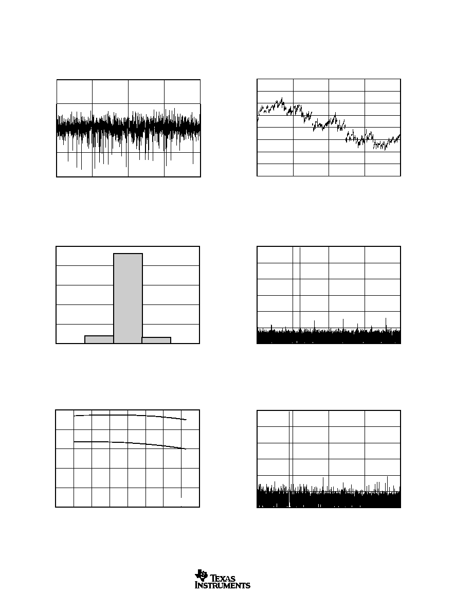
TYPICAL CHARACTERISTICS
At T
A
= full specified temperature range, V
S
= +5V, differential input range = 2V to 3V for each input, sampling rate = 32MSPS, unless otherwise noted.
0
≠20
≠40
≠60
≠80
≠100
≠120
SPECTRAL PERFORMANCE
(Differential, 2Vp-p)
0
4
8
12
16
Frequency (MHz)
Amplitude (dBFS)
f
IN
= 1MHz
SFDR = 73.5dBFS
SNR = 67.4dBFS
0
≠20
≠40
≠60
≠80
≠100
≠120
SPECTRAL PERFORMANCE
(Differential, 2Vp-p)
0
4
8
12
16
Frequency (MHz)
Amplitude (dBFS)
f
IN
= 10MHz
SFDR = 73.1dBFS
SNR = 66dBFS
0
≠20
≠40
≠60
≠80
≠100
≠120
SPECTRAL PERFORMANCE
(Differential, 3Vp-p)
0
4
8
12
16
Frequency (MHz)
Amplitude (dBFS)
f
IN
= 1MHz
SFDR = 71.3dBFS
SNR = 69.2dBFS
0
≠20
≠40
≠60
≠80
≠100
≠120
SPECTRAL PERFORMANCE
(Differential, 3Vp-p)
0
4
8
12
16
Frequency (MHz)
Amplitude (dBFS)
f
IN
= 10MHz
SFDR = 70.8dBFS
SNR = 67.9dBFS
0
≠20
≠40
≠60
≠80
≠100
≠120
2-TONE INTERMODULATION DISTORTION
0
4
8
12
16
Frequency (MHz)
Amplitude (dBFS)
f
1
= 9MHz (≠7dBFS)
f
2
= 10MHz (≠7dBFS)
IMD(3) = 74.6dBc
80
78
76
74
72
70
68
66
64
62
60
Frequency (MHz)
24
26
28
30
32
34
36
SNR, SFDR (dBFS)
DYNAMIC PERFORMANCE vs CLOCK
REF = 2V
f
IN
= 3.5MHz
SFDR
SNR

ADS2806
SBAS178B
7
www.ti.com
TYPICAL CHARACTERISTICS
(Cont.)
At T
A
= full specified temperature range, V
S
= +5V, differential input range = 2V to 3V for each input, sampling rate = 32MSPS, unless otherwise noted.
75
70
65
60
55
50
45
40
DYNAMIC PERFORMANCE vs INPUT FREQUENCY
1
10
100
Frequency (MHz)
Dynamic Performance (dBFS)
Power = ≠1dBFS
SFDR
THD
SNR
SINAD
0.5
0.25
0
≠0.25
≠0.5
DIFFERENTIAL LINEARITY ERROR
(Differential, 2Vp-p)
0
1024
2048
3072
4096
Code
DLE (LSB)
f
IN
= 10MHz
4
3
2
1
0
≠1
≠2
≠3
≠4
Code
0
1024
2048
3072
4096
f
IN
= 10MHz
ILE (LSB)
INTEGRAL LINEARITY ERROR
(Differential, 2Vp-p)
85
80
75
70
65
60
55
50
45
40
DYNAMIC PERFORMANCE vs INPUT FREQUENCY
1
10
100
Frequency (MHz)
Dynamic Performance (dBFS)
Power = ≠6dBFS
SFDR
THD
SNR
SINAD
100
90
80
70
60
50
40
30
20
10
0
SWEPT POWER (SFDR)
Input Amplitude (dBFS)
≠60
≠50
≠40
≠30
≠20
≠10
0
SFDR (dBFS, dBc)
f
IN
= 10MHz
dBFS
dBc
80
78
76
74
72
70
68
66
64
62
60
Clock (MHz)
24
26
28
30
32
34
36
SNR, SFDR (dBFS)
DYNAMIC PERFORMANCE vs CLOCK
REF = 3V
f
IN
= 3.5MHz
SFDR
SNR
ADS2806
SBAS178B
8
www.ti.com
TYPICAL CHARACTERISTICS
(Cont.)
At T
A
= full specified temperature range, V
S
= +5V, differential input range = 2V to 3V for each input, sampling rate = 32MSPS, unless otherwise noted.
0.5
0.25
0
≠0.25
≠0.5
DIFFERENTIAL LINEARITY ERROR
(Differential, 3Vp-p)
0
1024
2048
3072
4096
Code
DLE (LSB)
f
IN
= 10MHz
4
3
2
1
0
≠1
≠2
≠3
≠4
INTEGRAL LINEARITY ERROR
(Differential, 3Vp-p)
Code
0
1024
2048
3072
4096
f
IN
= 10MHz
ILE (LSB)
500k
400k
300k
200k
100k
OUTPUT NOISE HISTOGRAM (DC Input)
N-2
N-1
N
N+1
N+2
Code
Counts
3V Full Scale
0
≠20
≠40
≠60
≠80
≠100
≠120
Frequency (MHz)
0
4
8
12
16
f
IN
= 4.8MHz
Amplitude (dBFS)
CROSSTALK (Channel A)
0
≠20
≠40
≠60
≠80
≠100
≠120
Frequency (MHz)
0
4
8
12
16
f
IN
= 3.5MHz
Amplitude (dBFS)
CROSSTALK (Channel B)
75
70
65
60
55
50
DYNAMIC PERFORMANCE vs TEMPERATURE
≠60
≠40
≠20
0
20
40
60
80
100
Temperature (
∞
C)
SFDR, SNR (dBFS)
SFDR
SNR
f
IN
= 10MHz

ADS2806
SBAS178B
9
www.ti.com
APPLICATION INFORMATION
THEORY OF OPERATION
The ADS2806 integrates two high-speed CMOS ADCs and
an internal reference. The ADCs utilize a pipelined converter
architecture consisting of 11 internal stages. Each stage
feeds its data into the digital error correction logic, ensuring
excellent differential linearity and no missing codes at the
12-bit level. The output data becomes valid after the rising
clock edge (see Timing Diagram). The pipeline architecture
results in a data latency of 6 clock cycles.
The analog input of the ADS2806 consists of a differential
track-and-hold circuit. The differential topology along with
tightly matched poly-poly capacitors produce a high level of
AC performance at high sampling rates and in some under-
sampling applications.
Both inputs (IN, IN) require external biasing using a com-
mon-mode voltage that is typically at the mid-supply level
(+V
S
/2).
DRIVING THE ANALOG INPUTS
The analog inputs of the ADS2806 are very high impedance
and should be driven through an R-C network designed to
pass the highest frequency of interest. This prevents high-
frequency noise in the input from affecting SFDR and SNR.
The ADS2806 can be used in a wide variety of applications
and deciding on the best performing analog interface circuit
depends on the type of application. The circuit definition
should include considerations of input frequency spectrum
and amplitude, single-ended or differential drive, and avail-
able power supplies. For example, communication (fre-
quency domain) applications process frequency bands not
including DC. In imaging (time domain) applications, the
input DC component must be maintained into the ADC.
Features of the ADS2806 include full-scale select (SEL),
external reference, and CM output, providing flexibility to
accommodate a wide range of applications. The ADS2806
should be configured to meet application objectives, while
observing the headroom requirements of the driving ampli-
fiers, to yield the best overall performance.
The ADS2806 input structure allows it to be driven either
single-ended or differentially. Differential operation of the
ADS2806 requires an in-phase input signal and a 180
∞
out-
of-phase part simultaneously applied to the inputs (IN, IN ).
The differential operation offers a number of advantages
that, in most applications, will be instrumental in achieving
the best dynamic performance of the ADS2806:
∑ The signal swing is half of that required for the single-
ended operation and, therefore, is less demanding to
achieve while maintaining good linearity performance
from the signal source.
∑ The reduced signal swing allows for more headroom in
the interface circuitry and, therefore, a wider selection of
the best suitable driver op amp.
∑ Even-order harmonics are minimized.
∑ Improves the noise immunity based on the converter's
common-mode input rejection.
Using the single-ended mode, the signal is applied to one of
the inputs, while the other input is biased with a DC voltage
to the required common-mode level. Both inputs are equal
in terms of their impedance and performance, except that
applying the signal to the complementary input (IN) instead
of the IN input will invert the input signal relative to the
output code. For example, in the case when the input driver
operates in inverting mode, using IN as the signal input will
restore the phase of the signal to its original orientation.
Time-domain applications may benefit from a single-ended
interface configuration and its reduced circuit complexity.
Driving the ADS2806 with a single-ended signal will result in
a reduction of the distortion performance, while maintaining
good Signal-to-Noise Ratio (SNR). Employing dual-supply
amplifiers and AC-coupling will usually yield the best re-
sults, while DC-coupling and/or single-supply amplifiers
impose additional design constraints due to their headroom
requirements, especially when selecting the 3Vp-p input
range. However, single-supply amplifiers have the advan-
tage of inherently limiting their output swing to within the
supply rails. Alternatively, a voltage limiting amplifier, like
the OPA688, may be considered to set fixed-signal limits
and avoid any severe over-range condition for the ADC.
The full-scale input range of the ADS2806 is defined by the
reference voltages. For example, setting the range select
pin to SEL = LOW, and using the internal references
(REFT = +3.0V and REFTB = +2.0V), the full-scale range is
defined as: FSR = 2 ∑ (REFT ≠ REFB) = 2Vp-p.
The trade-off of the differential input configuration versus
the single-ended is its higher complexity. In either case, the
selection of the driver amplifier should be such that the
amplifier's performance will not degrade the ADC's perfor-
mance. The ADS2806 operates on a single power supply
that requires a level shift for ground-based bipolar input
signals to comply with its input voltage range requirements.
The input of the ADS2806 is of a capacitive nature and the
driving source needs to provide the current to charge or
discharge the input sampling capacitor while the track-and-
hold is in track mode. This effectively results in a dynamic
input impedance that depends on the sampling frequency.
In most applications, it is recommended to add a series
resistor, typically 20
to 50
, between the drive source and
the converter inputs. This will isolate the capacitive input
from the source, which can be crucial to avoid gain peaking
when using wideband operational amplifiers. Secondly, it
ADS2806
SBAS178B
10
www.ti.com
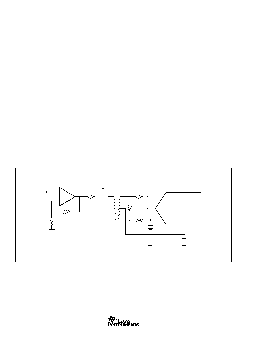
see matched impedances. Figure 1 shows the schematic for
the suggested transformer coupled interface circuit. The
component values of the R-C low-pass may be optimized
depending on the desired roll-off frequency. The resistor
across the secondary side (R
T
) should be calculated using
the equation R
T
= n
2
∑ R
G
to match the source impedance
(R
G
) for good power transfer and VSWR.
The circuit example of Figure 1 shows the voltage feedback
amplifier OPA680 driving the RF transformer, which con-
verts the single-ended signal into a differential. The OPA680
can be employed for either single- or dual-supply operation.
For details on how to optimize its frequency response, refer
to the OPA680 data sheet (SBOS083) on our web site at
www.ti.com. With the 49.9
series output resistor, the
amplifier emulates a 50
source (R
G
). Any DC content of
the signal can be easily blocked by a capacitor (0.1
µ
F) to
avoid DC loading of the op amp's output stage.
AC-Coupled, Single-Ended to Differential Interface
with Dual-Supply Op Amps
Some applications demand a very high dynamic range and
low levels of intermodulation distortion, but usually allow the
input signal to be AC-coupled into the ADC. Appropriate
driver amplifiers need to be selected to maintain the excellent
distortion performance of the ADS2806. Often, these op
amps deliver the lowest distortion with a small, ground-
centered signal swing that requires dual power supplies.
Because of the AC-coupling, this requirement can be easily
accomplished, and the needed level shifting of the input
signal can be implemented without affecting the driver circuit.
will create a 1st-order, low-pass filter in conjunction with the
specified input capacitance of the ADS2806. Its cutoff fre-
quency can be adjusted even further by adding an external
shunt capacitor from each signal input to ground. The
optimum values of this R-C network depend on a variety of
factors that include the ADS2806 sampling rate, the se-
lected op amp, the interface configuration, and the particular
application (time domain versus frequency domain). Gener-
ally, increasing the size of the series resistor and/or capaci-
tor will improve the SNR performance, but depending on the
signal source, large resistor values may be detrimental to
achieving good harmonic distortion. In any case, optimizing
the R-C values for the specific application is encouraged.
Transformer Coupled, Single-Ended to Differential
Configuration
If the application requires a signal conversion from a single-
ended source to drive the ADS2806 differentially, an RF
transformer might be a good solution. The selected trans-
former must have a center tap in order to apply the com-
mon-mode DC voltage necessary to bias the converter
inputs. AC grounding the center tap will generate the differ-
ential signal swing across the secondary winding. Consider
a step-up transformer to take advantage of a signal ampli-
fication without the introduction of another noise source.
Furthermore, the reduced signal swing from the source may
lead to improved distortion performance.
The differential input configuration provides the noticeable
advantage of achieving high SFDR over a wide range of
input frequencies. In this mode, both inputs of the ADS2806
FIGURE 1, Converting a Single-Ended Input Signal into a Differential Signal Using an RF-Transformer.
V
IN
IN
IN
CM
+2.5V
24.9
24.9
10
µ
F
0.1
µ
F
47pF
R
T
47pF
1:n
0.1
µ
F
R
G
R
2
R
1
OPA680
49.9
1/2
ADS2806Y
+
One Channel of Two
ADS2806
SBAS178B
11
www.ti.com
Figure 2 shows an example of such an interface circuit
specifically designed to maximize the dynamic performance.
The voltage feedback amplifier, OPA642, maintains an
excellent distortion performance for input frequencies of up
to 15MHz. The two amplifiers (A1, A2) are configured as an
inverting and noninverting gain stage to convert the input
signal from single-ended to differential. The nominal gain for
this stage is set to +2V/V. The outputs of the OPA642s are
AC-coupled to the converter's differential inputs. This will
keep the distortion performance at its best since the signal
range stays within the linear region of the op amp and
sufficient headroom to the supply rails can be maintained.
Four resistors located between the top (REFT) and bottom
(REFB) reference shift the input signal to a common-mode
voltage of approximately +2.5V.
The interface circuit of Figure 2 can be modified to extend
the bandwidth to approximately 25MHz, by replacing the
OPA642 with its decompensated version, the OPA643. The
OPA643 provides the necessary slew rate for a low distor-
FIGURE 2. AC-Coupled Differential Driver Interface with OPA642.
FIGURE 3. AC-Coupled, Differential Interface for Single-Supply Operation.
V
IN
1/2
ADS2806Y
100pF
IN
IN
402
1.82k
1.82k
16.5
200
402
402
REFB
100pF
0.1
µ
F
0.1
µ
F
A1
OPA642
A2
OPA642
REFT
1.82k
1.82k
16.5
One Channel of Two
V
IN
1/2
ADS2806Y
68pF
IN
CM
IN
+5V
68pF
0.1
µ
F
0.1
µ
F
0.1
µ
F
1/2
OPA2681
1/2
OPA2681
R
G
249
R
F
499
499
R
S
24.9
V
CM
= +2.5V
R
P
499
R
P
499
R
F
499
R
IN
249
R
S
24.9
One Channel of Two
tion front end to the ADS2806. With a minimum gain stability
of +3, the gain resistors have to be modified, as well as
optimizing the series resistor and shunt capacitance at each
of the converter inputs.
AC-Coupled, Single-Ended-to-Differential Interface
for Single-Supply Operation
The previously discussed interface circuit can be modified if
the system only allows for a single-supply operation, e.g.,
V
S
= +5V. Single-supply operation requires the driver ampli-
fier to be biased as well in order to process a bipolar input
signal. Typically, single-supply amplifiers do not achieve
distortion performance as well as dual-supply op amps. The
driver amplifier's output swing must exceed the full-scale
input range of the converter. In addition, dual op amps, such
as the current-feedback OPA2681, should be considered
since they provide the closest open-loop gain and phase
matching between the two channels. Shown in Figure 3 is
a single-supply interface circuit for an AC-coupled input
signal. With the ADS2806 set to the 2Vp-p input range, the
ADS2806
SBAS178B
12
www.ti.com
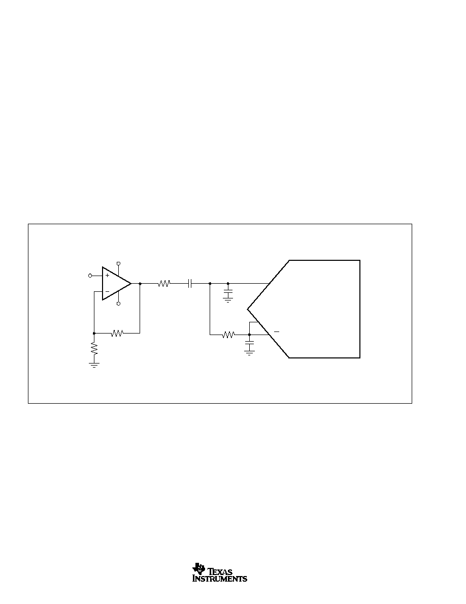
FIGURE 4. AC-Coupling the Dual-Supply Amplifier OPA642 to the ADS2806 for a 2Vp-p Full-Scale Input Range.
OPA642
V
IN
R
F
402
R
G
402
1/2
ADS2806Y
R
S
16.5
68pF
0.1
µ
F
0.1
µ
F
IN
IN
CM
+5V
≠5V
1.82k
One Channel of Two
top and bottom references (REFT, REFB) provide an output
voltage of +3.0V and +2.0V, respectively. The CM output of
the ADS2806 is used to bias the inputs of the driving
amplifiers. Using the OPA2681 on a single +5V supply, its
ideal common-mode point is +2.5V, which coincides with
the recommended common-mode input level for the
ADS2806, thus eliminating the need for coupling capacitors
between the amplifiers and the converter.
The addition of a small series resistor (R
S
) between the
output of the op amps and the input of the ADS2806 will be
beneficial in almost all interface configurations. It will de-
couple the op amp's output from the capacitive load and
avoid gain peaking that can result in increased noise. For
best spurious and distortion performance, the resistor value
should be kept below 100
. Furthermore, the series resis-
tor, in combination with the shunt capacitor, establishes a
passive low-pass filter limiting the bandwidth for the wideband
noise, thus improving the SNR. The spurious-free dynamic
range of this single-supply front end is limited by the 2nd-
harmonic distortion. An improvement of several dB may be
realized by adding a pull-down resistor (R
P
) at the output of
each amplifier. This pulls a DC bias current out of the output
stage of the amplifier. It is set to approximately 5mA, see
Figure 3, but will vary depending on the amplifier used.
Single-Ended, AC-Coupled, Dual-Supply Interface
The circuit provided in Figure 4 shows typical connections
for using the ADS2806 in a single-ended input configura-
tion. The bias requirements for AC-coupling are provided by
a single resistor to the CM output lead. The single-ended
mode of operation should be considered for ease of inter-
face complexity and applications where the dynamic perfor-
mance can be compromised. The series resistor R
S
, along
with the shunt capacitance, provide the means to adjust the
bandwidth and optimize the performance towards good
signal-to-noise ratio. In addition, the amplifier configuration
can be easily modified for an anti-aliasing filter based on a
2nd-order Sallen-Key or Multiple-Feedback topology.
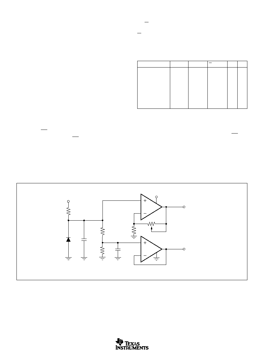
The interface example, shown in Figure 4, operates with the
full-scale range of the ADS2806 set to 2Vp-p, leaving
sufficient headroom for the output of the OPA642 to drive
the converter and maintain low signal distortion.
ADS2806
SBAS178B
13
www.ti.com
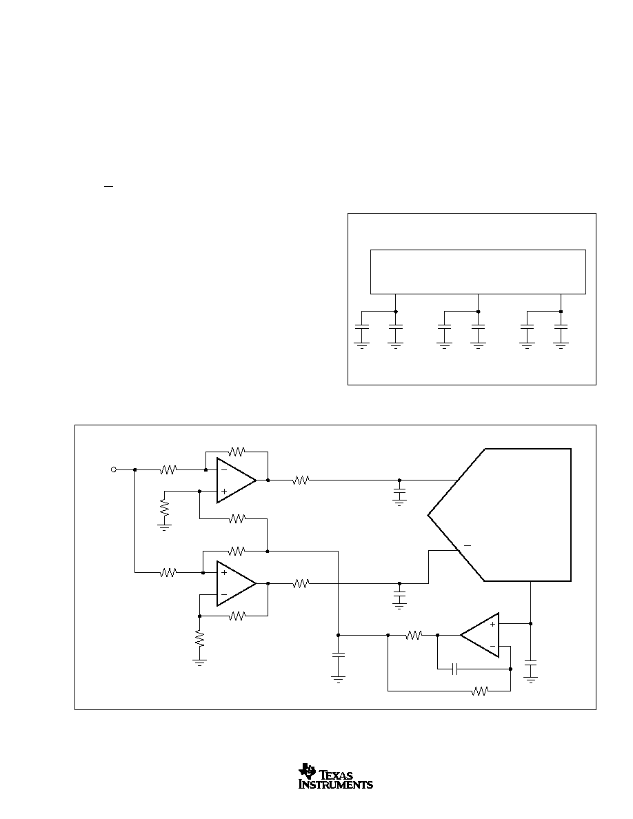
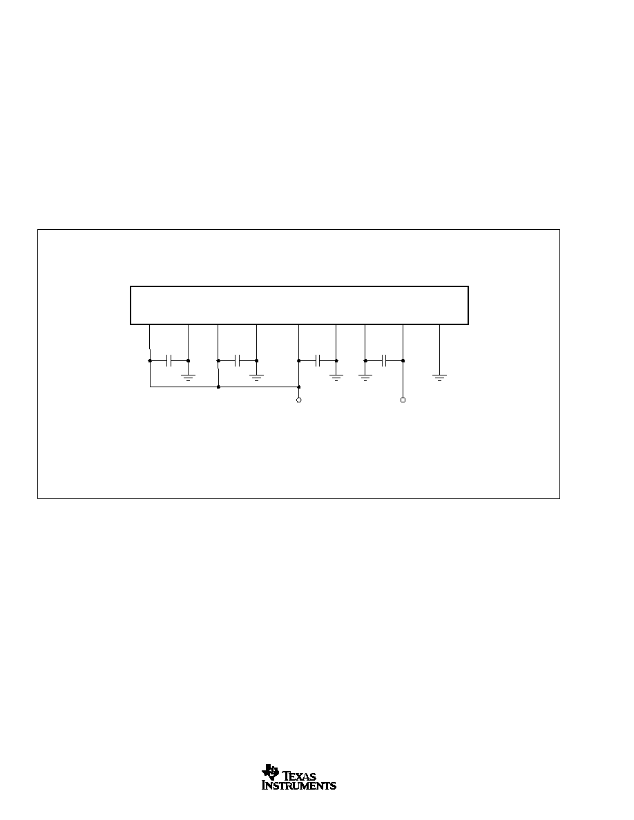
FIGURE 6. Recommended Bypassing for the Reference Pins.
FIGURE 5. DC-Coupled Input Driver with Level Shifting.
V
IN
1/2
ADS2806Y
IN
IN
CM
499
249
24.9
24.9
249
1/2
OPA2681
1/2
OPA2681
0.1
µ
F
0.1
µ
F
0.1
µ
F
499
499
499
249
249
24.9
1k
22pF
22pF
OPA234
One Channel of Two
REFT
CM
0.1
µ
F
REFB
1/2
ADS2806
0.1
µ
F
0.1
µ
F
10
µ
F
+
10
µ
F
+
10
µ
F
+
DC-Coupled, Differential Driver with Level Shift
Several applications will require that the bandwidth of the
signal path include DC, in which case, the signal has to be
DC-coupled to the ADC. An op amp based interface circuit
can be configured to scale and level shift the input signal to
be compatible with the selected input range of the ADC. The
circuit shown in Figure 5 employs a dual op amp, OPA2681,
to drive the input of the ADS2806 differentially. The single-
supply, general-purpose op amp OPA234 is added to buffer
the common-mode voltage of +2.5V, available at the CM pin,
and apply it to the input of the driver amplifier. This sets the
correct DC voltage to bias the inputs of the ADS2806. It
should be noted that any DC voltage differences between the
IN and IN inputs of the ADS2806 will result in an offset error.
Using the OPA2681, this circuit can be operated either with
a single or a dual
±
5V supply.
REFERENCE OPERATION
The internal reference consists of a bandgap voltage refer-
ence, the drivers for the top and bottom reference, and the
resistive reference ladder. References are internally con-
nected, e.g.: REFT
A
is connected to REFT
B
, and REFB
A
is
connected to REFB
B
. The bandgap reference circuit includes
logic functions that allow setting the analog input swing of the
ADS2806 to a differential full-scale range of either 2Vp-p or
3Vp-p by simply tying the SEL pin to a LOW or HIGH
potential, respectively. While operating the ADS2806 in the
external reference mode, the buffer amplifiers for REFT and
REFB are disabled. The ADS2806 has an internal 50k
pull-
down resistor at the range select pin (SEL). Therefore, this pin
can be either hardwired to ground or left unconnected, which
will default the converter to a 2Vp-p full-scale input range
(FSR). While set for the 2Vp-p range, the top and bottom
reference voltages will be REFT = +3.0V and REFB = +2.0V.
Switching to the 3Vp-p range changes those voltages to
REFT = +3.25V and REFB = +1.75V. The reference buffers
can be utilized to supply up to 1mA/channel (2mA total, sink
and source) to external circuitry. To ensure proper operation
with any reference configuration, it is necessary to provide
solid bypassing at all reference pins in order to keep the clock
feedthrough to a minimum, as shown in Figure 6. Good
performance requires using 0.1
µ
F low inductance capacitors.
All bypassing capacitors should be located as close to their
respective pins as possible.
ADS2806
SBAS178B
14
www.ti.com
FIGURE 7. Example for an External Reference Driver Using the Dual, Single-Supply Op Amp, OPA2234.
OPA2234
A1
OPA2234
A2
R
3
R
4
R
2
R
1
+5V
+5V
0.1
µ
F
10
µ
F
> 1.70V
< 3.30V
Top Reference
Bottom Reference
+
4.7k
REF1004
+2.5V
One Channel of Two
USING EXTERNAL REFERENCES
For even more design flexibility, the internal reference can
be disabled and an external reference voltage used. Driving
both channels with an external reference offers the best
performance, as it allows the channels to maintain balance.
The utilization of an external reference may be considered
for applications requiring higher accuracy, improved tem-
perature performance, or a wide adjustment range of the
converter's full-scale range. In multichannel applications,
the use of a common external reference has the benefit of
obtaining better matching and drift of the full-scale range
between converters. Figure 7 gives an example of an
external reference circuit using a single-supply, low-power,
dual op amp (OPA2234).
The external references can vary as long as the value of the
external top reference (REFT) stays within the range of
V
S
≠ 1.70V and REFB + 0.4V, and the external bottom
reference (REFB) stays within 1.70V and REFT ≠ 0.4V.
Note that the function of the range selector pin (SEL) is
disabled while the converter operates in external reference
mode. Setting the ADS2806 for external reference mode
requires the INT/EXT pin (pin 18) to be HIGH.
The logic level applied to the INT/EXT pin of the ADS2806
determines if the converter operates with either the built-in
reference or external reference voltages. Due to this func-
tion pin having an internal 50k
pull-up resistor, the default
configuration is external reference mode. Grounding this pin
will activate the internal reference option.
The input track-and-hold amplifier is differential. A positive
1Vp-p on the IN and its compliment, a negative 1Vp-p, on
the IN (see Figure 3) results in 2Vp-p on the output of the
track-and-hold. Likewise, 2Vp-p on the IN and 0Vp-p on the
IN (see Figure 4) results in 2Vp-p on the output of the track-
and-hold. Therefore, the reference voltages, REFT and
REFB, are the same for both differential and single-ended
inputs, as shown in Table I.
The external references may be changed for different tasks.
The ADS2806 will follow the external references with a
latency of 8 to 10 clock cycles. If it is desired to use INT/EXT
and SEL to change the configuration of a circuit for different
tasks, a large amount of time must be allowed. This time
could be hundreds of microseconds. Refer to the Diagram
on the front page. Note that there is no disconnect for
external references. If it is desired to switch between inter-
nal and external references, disconnect switches must be
added between the external references and the ADS2806.
INPUT
REFERENCE IN (Pin-50, 63) IN (Pin-51, 62)
REFT
REFB
2Vp-p Differential
Internal
2V to 3V
3V to 2V
+3V
+2V
1Vp-p Times 2 Inputs
or External
2Vp-p Single-Ended
Internal
1.5V to 3.5V
2.5V
DC
+3V
+2V
2Vp-p Times 1 Input
or External
3Vp-p Differential
Internal
1.75V to 3.35V 3.25V to 1.75V +3.25V +1.75V
1.5Vp-p Times 2 Inputs
or External
3Vp-p Single-Ended
Internal
1V to 4V
2.5V
DC
+3.25V +1.75V
3Vp-p Times 1 Input
or External
TABLE I. Reference Voltages for Input Signal Ranges.

ADS2806
SBAS178B
15
www.ti.com
TABLE II. Coding Table for Single-Ended Input Configuration
with IN Tied to the Common-Mode Voltage.
SINGLE-ENDED INPUT
STRAIGHT OFFSET BINARY
(IN = CM, Pins 52, 61)
(SOB)
+FS≠1LSB (IN = CMV + FSR/2)
1111 1111 1111
+1/2 FS
1100 0000 0000
Bipolar Zero (IN = V
CM
)
1000 0000 0000
≠1/2 FS
0100 0000 0000
≠FS (IN = CMV ≠ FSR/2)
0000 0000 0000
TABLE III. Coding Table for Differential Input Configuration.
STRAIGHT OFFSET BINARY
DIFFERENTIAL INPUT
(SOB)
+FS≠1LSB (IN = +3V, IN = +2V)
1111 1111 1111
+1/2 FS
1100 0000 0000
Bipolar Zero (IN = IN = V
CM
)
1000 0000 0000
≠1/2 FS
0100 0000 0000
≠FS (IN = +2V, IN = +3V)
0000 0000 0000
DIGITAL INPUTS AND OUTPUTS
Clock Input Requirements
Both channels of the ADS2806 are controlled by the same
clock on the rising edge. Utilizing a single clock reduces
timing uncertainty in the sampling of the two channels.
Clock jitter is critical to the SNR performance of high-speed,
high-resolution ADCs. Clock jitter leads to aperture jitter (t
A
),
which adds noise to the signal being converted. The
ADS2806 samples the input signal on the rising edge of the
CLK input. Therefore, this edge should have the lowest
possible jitter. The jitter noise contribution to total SNR is
given by the following equation. If this value is near your
system requirements, input clock jitter must be reduced.
Jitter SNR
rms signal to rms noise
=
20 log
1
2
t
IN
A
where:
IN
is input signal frequency
t
A
is rms clock jitter
Particularly in undersampling applications, special consider-
ation should be given to clock jitter. The clock input should be
treated as an analog input in order to achieve the highest
level of performance. Any overshoot or undershoot of the
clock signal may cause degradation of the performance.
When digitizing at high sampling rates, the clock should have
50% duty cycle (t
H
= t
L
), along with fast rise and fall times of
2ns or less. The clock input of the ADS2806 can be driven
with either 3V or 5V logic levels. Using low-voltage logic (3V)
may lead to improved AC performance of the converter.
Over Range Indicator (OVR)
If the analog input voltage exceeds the set full-scale range,
an over range condition exists. The "OVR" pin of the ADS2806
can be used to monitor any such out-of-range condition. This
"OVR" output is updated along with the data output corre-
sponding to the particular sampled analog input voltage.
Therefore, the OVR data is subject to the same pipeline
delay as the digital data. The OVR output is LOW when the
input voltage is within the defined input range. It will go HIGH
if the applied signal exceeds the full-scale range.
Data Outputs
The digital outputs of the ADS2806 can be set to a high-
impedance state by driving OE (pins 6 and 42) with a logic
HIGH. Normal operation is achieved with pins 6 and 42
LOW due to internal pull-down resistors. This function is
provided for testability purposes and is not meant to drive
digital buses directly, or be dynamically changed during the
conversion process. The output data format of the ADS2806
is in positive Straight Offset Binary code, as shown in
Tables II and III. This format can easily be converted into the
Binary Two's Complement code by inverting the MSB.
Data output is in the form of two parallel words. It is
recommended that the capacitive loading on the data lines
be as low as possible (< 15pF). Higher capacitive loading
will cause larger dynamic currents as the digital outputs are
changing. Those high current surges can feed back to the
analog portion of the ADS2806 and affect the performance.
If necessary, external buffers or latches close to the
converter's output pins may be used to minimize the capaci-
tive loading. They also provide the added benefit of isolating
the ADS2806 from high-frequency digital noise on the bus
coupling back into the converter.
Digital Output Driver Supply (VDRV)
Each channel of the ADS2806 has a separate dedicated
supply pin (8, 40) for the output logic drivers, VDRV, which
are not internally connected to the other supply pins. Setting
the voltage at VDRV to +5V or +3V, the ADS2806 produces
corresponding logic levels and can directly interface to the
selected logic family. The output stages are designed to
supply sufficient current to drive a variety of logic families.
However, it is recommended to use the ADS2806 with +3V
logic supply. This will lower the power dissipation in the
output stages due to the lower output swing and reduce
current glitches on the supply line that may affect the AC
performance of the converter. In some applications, it might
be advantageous to decouple the VDRV pin with additional
capacitors or a pi-filter.
OUTPUT ENABLE (
OE
)
The digital outputs of the ADS2806 can be set to high
impedance (tri-state) by driving OE
A
and OE
B
(pins 6, 42)
with a logic HIGH. Normal operation is achieved with the
same pins pulled LOW.
ADS2806
SBAS178B
16
www.ti.com
FIGURE 8. Recommended Bypassing for the Supply Pins.
GROUNDING AND DECOUPLING
Proper grounding, bypassing, short trace lengths, and the
use of power and ground planes are particularly important
for high-frequency designs. Multilayer PC boards are rec-
ommended for best performance since they offer distinct
advantages, such as minimizing ground impedance, sepa-
ration of signal layers by ground layers, etc. The ADS2806
should be treated as an analog component. Whenever
possible, the supply pins should be powered by the analog
supply. This will ensure the most consistent results, since
digital supply lines often carry high levels of noise that
otherwise would be coupled into the converter and degrade
the achievable performance. The ground pins should di-
rectly connect to an analog ground plane that covers the PC
board area under the converter. While designing the layout
+V
S
57
GND
55, 58
+V
S
3 (46)
GND
1, 2, 64
(47, 48, 49)
+V
S
5 (43)
GND
4 (44)
ADS2806
0.1
µ
F
GND
23, 25
0.1
µ
F
0.1
µ
F
GND
7 (41)
VDRV
8 (40)
0.1
µ
F
+3V/+5V
+5V
Numbers in Parenthesis Indicate Pins for Channel A
it is important to keep the analog signal traces separated
from any digital lines to prevent noise coupling onto the
analog signal path. Due to its high sampling rate, the
ADS2806 generates high-frequency current transients and
noise (clock feedthrough) that are fed back into the supply
and reference lines. This requires that all supply and refer-
ence pins are sufficiently bypassed. Figure 8 shows the
recommended decoupling scheme for the ADS2806. In
most cases, 0.1
µ
F ceramic chip capacitors at each pin are
adequate to keep the impedance low over a wide frequency
range. Their effectiveness largely depends on the proximity
to the individual supply pin. Therefore, they should be
located as close to the supply pins as possible. If system
supplies are not a low enough impedance, adding a small
tantalum capacitor will yield the best results.
ADS2806
SBAS178B
17
www.ti.com
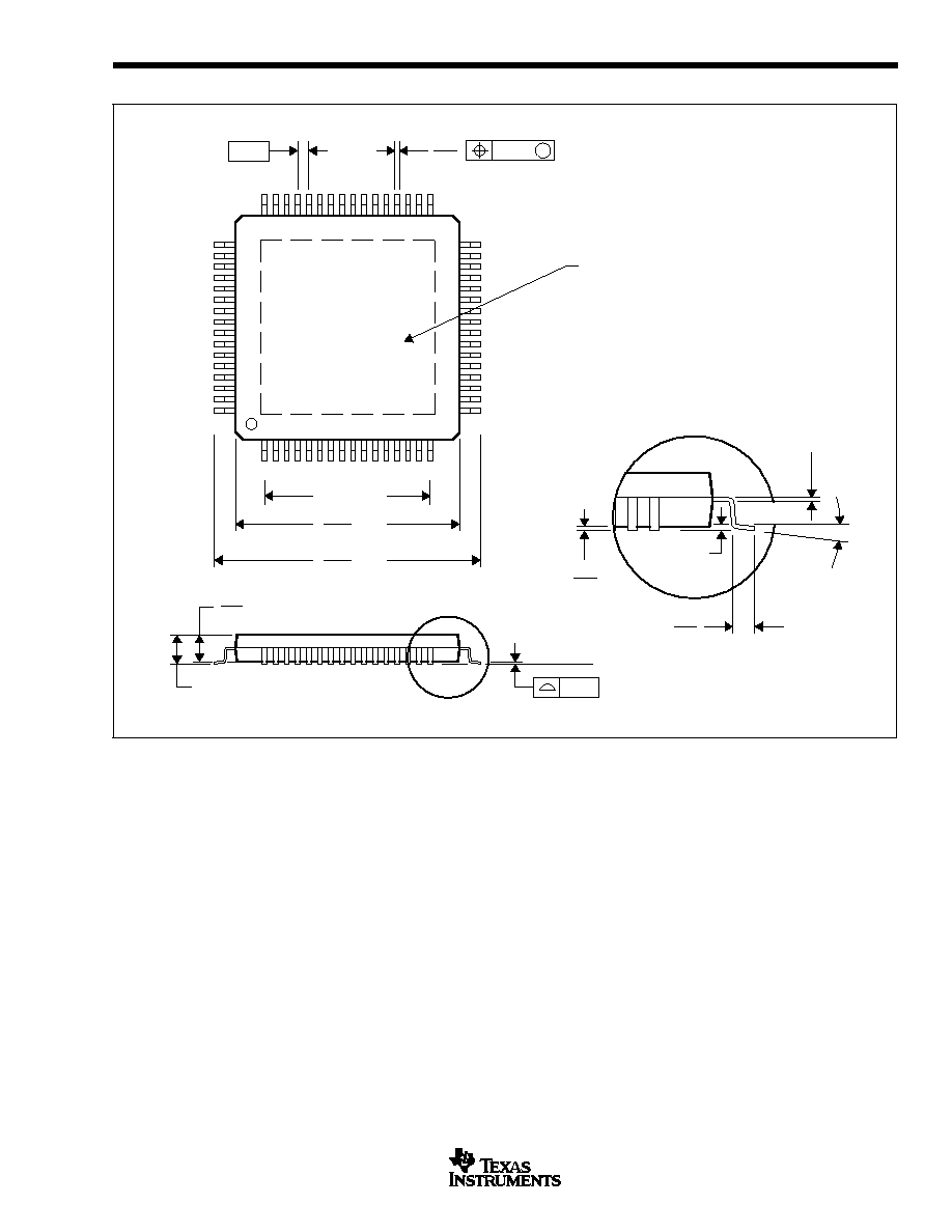
PACKAGE DRAWING
MPQF071 ≠ JANUARY 1998
PAP (S-PQFP-G64)
PowerPAD
PLASTIC QUAD FLATPACK
Thermal Pad
(See Note D)
0,13 NOM
0,25
0,45
0,75
Seating Plane
4147702/A 01/98
Gage Plane
0,17
0,27
33
16
48
1
7,50 TYP
49
64
SQ
9,80
1,05
0,95
11,80
12,20
1,20 MAX
10,20
SQ
17
32
0,08
0,50
M
0,08
0
∞
≠ 7
∞
0,15
0,05
NOTES: A. All linear dimensions are in millimeters.
B. This drawing is subject to change without notice.
C. Body dimensions do not include mold flash or protrusion.
D. The package thermal performance may be enhanced by bonding the thermal pad to an external thermal plane.
This pad is electrically and thermally connected to the backside of the die and possibly selected leads.
E. Falls within JEDEC MS-026

PACKAGING INFORMATION
ORDERABLE DEVICE
STATUS(1)
PACKAGE TYPE
PACKAGE DRAWING
PINS
PACKAGE QTY
ADS2806Y/1K5
ACTIVE
HTQFP
PAP
64
1500
ADS2806Y/250
ACTIVE
HTQFP
PAP
64
250
(1) The marketing status values are defined as follows:
ACTIVE: Product device recommended for new designs.
LIFEBUY: TI has announced that the device will be discontinued, and a lifetime-buy period is in effect.
NRND: Not recommended for new designs. Device is in production to support existing customers, but TI does not recommend using this part in
a new design.
PREVIEW: Device has been announced but is not in production. Samples may or may not be available.
OBSOLETE: TI has discontinued the production of the device.
PACKAGE OPTION ADDENDUM
www.ti.com
3-Oct-2003

IMPORTANT NOTICE
Texas Instruments Incorporated and its subsidiaries (TI) reserve the right to make corrections, modifications,
enhancements, improvements, and other changes to its products and services at any time and to discontinue
any product or service without notice. Customers should obtain the latest relevant information before placing
orders and should verify that such information is current and complete. All products are sold subject to TI's terms
and conditions of sale supplied at the time of order acknowledgment.
TI warrants performance of its hardware products to the specifications applicable at the time of sale in
accordance with TI's standard warranty. Testing and other quality control techniques are used to the extent TI
deems necessary to support this warranty. Except where mandated by government requirements, testing of all
parameters of each product is not necessarily performed.
TI assumes no liability for applications assistance or customer product design. Customers are responsible for
their products and applications using TI components. To minimize the risks associated with customer products
and applications, customers should provide adequate design and operating safeguards.
TI does not warrant or represent that any license, either express or implied, is granted under any TI patent right,
copyright, mask work right, or other TI intellectual property right relating to any combination, machine, or process
in which TI products or services are used. Information published by TI regarding third-party products or services
does not constitute a license from TI to use such products or services or a warranty or endorsement thereof.
Use of such information may require a license from a third party under the patents or other intellectual property
of the third party, or a license from TI under the patents or other intellectual property of TI.
Reproduction of information in TI data books or data sheets is permissible only if reproduction is without
alteration and is accompanied by all associated warranties, conditions, limitations, and notices. Reproduction
of this information with alteration is an unfair and deceptive business practice. TI is not responsible or liable for
such altered documentation.
Resale of TI products or services with statements different from or beyond the parameters stated by TI for that
product or service voids all express and any implied warranties for the associated TI product or service and
is an unfair and deceptive business practice. TI is not responsible or liable for any such statements.
Following are URLs where you can obtain information on other Texas Instruments products and application
solutions:
Products
Applications
Amplifiers
amplifier.ti.com
Audio
www.ti.com/audio
Data Converters
dataconverter.ti.com
Automotive
www.ti.com/automotive
DSP
dsp.ti.com
Broadband
www.ti.com/broadband
Interface
interface.ti.com
Digital Control
www.ti.com/digitalcontrol
Logic
logic.ti.com
Military
www.ti.com/military
Power Mgmt
power.ti.com
Optical Networking
www.ti.com/opticalnetwork
Microcontrollers
microcontroller.ti.com
Security
www.ti.com/security
Telephony
www.ti.com/telephony
Video & Imaging
www.ti.com/video
Wireless
www.ti.com/wireless
Mailing Address:
Texas Instruments
Post Office Box 655303 Dallas, Texas 75265
Copyright
2003, Texas Instruments Incorporated