 | –≠–ª–µ–∫—Ç—Ä–æ–Ω–Ω—ã–π –∫–æ–º–ø–æ–Ω–µ–Ω—Ç: ADS7809P | –°–∫–∞—á–∞—Ç—å:  PDF PDF  ZIP ZIP |
©
1992 Burr-Brown Corporation
PDS-1154D
Printed in U.S.A., November, 1996
ADS7809
ADS7809
Æ
ADS7809
International Airport Industrial Park ∑ Mailing Address: PO Box 11400, Tucson, AZ 85734 ∑ Street Address: 6730 S. Tucson Blvd., Tucson, AZ 85706 ∑ Tel: (520) 746-1111 ∑ Twx: 910-952-1111
Internet: http://www.burr-brown.com/ ∑ FAXLine: (800) 548-6133 (US/Canada Only) ∑ Cable: BBRCORP ∑ Telex: 066-6491 ∑ FAX: (520) 889-1510 ∑ Immediate Product Info: (800) 548-6132
16-Bit 10
µ
s Serial CMOS Sampling
ANALOG-to-DIGITAL CONVERTER
FEATURES
q
100kHz SAMPLING RATE
q
86dB SINAD WITH 20kHz INPUT
q
±
2 LSB INL
q
DNL: 16 BITS "No Missing Codes"
q
SIX SPECIFIED INPUT RANGES
q
SERIAL OUTPUT
q
SINGLE +5V SUPPLY OPERATION
q
PIN-COMPATIBLE WITH 12-BIT ADS7808
q
USES INTERNAL OR EXTERNAL
REFERENCE
q
100mW MAX POWER DISSIPATION
q
20-PIN 0.3" PLASTIC DIP AND SOIC
q
SIMPLE DSP INTERFACE
DESCRIPTION
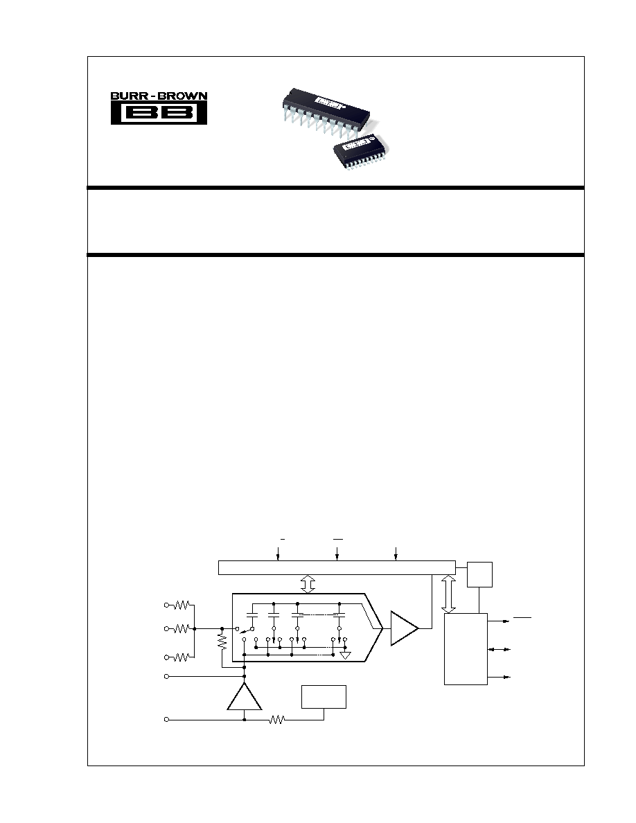
The ADS7809 is a complete 16-bit sampling analog-
to-digital using state-of-the-art CMOS structures. It
contains a 16-bit capacitor-based SAR A/D with S/H,
reference, clock, and a serial data interface. Data can
be output using the internal clock, or can be synchro-
nized to an external data clock. The ADS7809 also
provides an output synchronization pulse for ease of
use with standard DSP processors.
The ADS7809 is specified at a 100kHz sampling rate,
and guaranteed over the full temperature range. Laser-
trimmed scaling resistors provide various input ranges
including
±
10V and 0V to 5V, while an innovative
design operates from a single +5V supply, with power
dissipation under 100mW.
The 20-pin ADS7809 is available in a plastic 0.3" DIP
and in an SOIC, both fully specified for operation over
the industrial ≠40
∞
C to +85
∞
C range.
10k
CDAC
4k
20k
5k
Internal
+2.5V Ref
Clock
BUSY
Data Clock
Serial Data
Successive Approximation Register and Control Logic
Serial
Data
Out
Comparator
Buffer
20k
R/C
CS
Power
Down
R1
IN
R2
IN
R3
IN
REF
CAP
DEMO BOARD
AVAILABLE

Æ
ADS7809
2
The information provided herein is believed to be reliable; however, BURR-BROWN assumes no responsibility for inaccuracies or omissions. BURR-BROWN
assumes no responsibility for the use of this information, and all use of such information shall be entirely at the user's own risk. Prices and specifications are subject
to change without notice. No patent rights or licenses to any of the circuits described herein are implied or granted to any third party. BURR-BROWN does not
authorize or warrant any BURR-BROWN product for use in life support devices and/or systems.
SPECIFICATIONS
ELECTRICAL
At T
A
= ≠40
∞
C to +85
∞
C, f
S
= 100kHz, V
DIG
= V
ANA
= +5V, using internal reference and fixed resistors as shown in Figure 4, unless otherwise specified.
ADS7809P, U
ADS7809PB, UB
PARAMETER
CONDITIONS
MIN
TYP
MAX
MIN
TYP
MAX
UNITS
RESOLUTION
16
T
Bits
ANALOG INPUT
Voltage Ranges
±
10, 0V to 5V, etc. (See Table I)
Impedance
See Table I
Capacitance
35
T
pF
THROUGHPUT SPEED
Complete Cycle
Acquire and Convert
10
T
µ
s
Throughput Rate
100
T
kHz
DC ACCURACY
Integral Linearity Error
±
3
±
2
LSB
(1)
Differential Linearity Error
+3, ≠2
±
1
LSB
No Missing Codes
15
16
Bits
Transition Noise
(2)
1.3
T
LSB
Full Scale Error
(3,4)
±
0.5
T
%
Full Scale Error Drift
±
7
T
ppm/
∞
C
Full Scale Error
(3,4)
Ext. 2.5000V Ref
±
0.5
T
%
Full Scale Error Drift
Ext. 2.5000V Ref
±
2
T
ppm/
∞
C
Bipolar Zero Error
(3)
Bipolar Ranges
±
10
T
mV
Bipolar Zero Error Drift
Bipolar Ranges
±
2
T
ppm/
∞
C
Unipolar Zero Error
(3)
0V tp 10V Ranges
±
5
T
mV
Unipolar Zero Error
(3)
0V to 4V, 0V to 5V Ranges
±
3
T
mV
Unipolar Zero Error Drift
Unipolar Ranges
±
2
T
ppm/
∞
C
Recovery to Rated Accuracy
1
µ
F Capacitor to CAP
1
T
ms
after Power Down
Power Supply Sensitivity
+4.75V < V
D
< +5.25V
±
8
T
LSB
(V
DIG
= V
ANA
= V
D
)
AC ACCURACY
Spurious-Free Dynamic Range
f
IN
= 20kHz
90
100
96
T
dB
(5)
Total Harmonic Distortion
f
IN
= 20kHz
≠100
≠90
T
≠94
dB
Signal-to-(Noise+Distortion)
f
IN
= 20kHz
83
88
86
T
dB
≠60dB Input
30
32
dB
Signal-to-Noise
f
IN
= 20kHz
83
88
86
T
dB
Full-Power Bandwidth
(6)
250
T
kHz
SAMPLING DYNAMICS
Aperture Delay
40
T
ns
Transient Response
FS Step
2
T
µ
s
Overvoltage Recovery
(7)
150
T
ns
REFERENCE
Internal Reference Voltage
No Load
2.48
2.5
2.52
T
T
T
V
Internal Reference Source Current
1
T
µ
A
(Must use external buffer)
External Reference Voltage Range
2.3
2.5
2.7
T
T
T
V
For Specified Linearity
External Reference Current Drain
Ext. 2.5000V Ref
100
T
µ
A
DIGITAL INPUTS
Logic Levels
V
IL
≠0.3
+0.8
T
T
V
V
IH
+2.0
V
D
+0.3V
T
T
V
I
IL
V
IL
= 0V
±
10
T
µ
A
I
IH
V
IH
= 5V
±
10
T
µ
A

Æ
ADS7809
3
SPECIFICATIONS
(CONT)
ELECTRICAL
At T
A
= ≠40
∞
C to +85
∞
C, f
S
= 100kHz, V
DIG
= V
ANA
= +5V, using internal reference and fixed resistors as shown in Figure 4, unless otherwise specified.
ADS7809P, U
ADS7809PB, UB
PARAMETER
CONDITIONS
MIN
TYP
MAX
MIN
TYP
MAX
UNITS
DIGITAL OUTPUTS
Data Format
Serial 16 bits
Data Co
Binary Two's Complement or Straight Binary
Pipeline Delay
Conversion results only available after completed conversion.
Data Clock
Selectable for internal or external data clock
Internal
EXT/INT LOW
2.3
T
MHz
(Output Only When
Transmitting Data)
External
EXT/INT HIGH
0.1
10
T
T
MHz
(Can Run Continually)
V
OL
I
SINK
= 1.6mA
+0.4
T
V
V
OH
I
SOURCE
= 500
µ
A
+4
T
V
Leakage Current
High-Z State,
±
5
T
µ
A
V
OUT
= 0V to V
DIG
Output Capacitance
High-Z State
15
T
pF
POWER SUPPLIES
Specified Performance
V
DIG
Must be
V
ANA
+4.75
+5
+5.25
T
T
T
V
V
ANA
+4.75
+5
+5.25
T
T
T
V
I
DIG
0.3
T
mA
I
ANA
16
T
mA
Power Dissipation: PWRD LOW
V
ANA
= V
DIG
= 5V, f
S
= 100kHz
100
T
mW
PWRD HIGH
50
T
µ
W
TEMPERATURE RANGE
Specified Performance
≠40
+85
T
T
∞
C
Derated Performance
≠55
+125
T
T
∞
C
Storage
≠65
+150
T
T
∞
C
Thermal Resistance (
JA
)
Plastic DIP
75
T
∞
C/W
SOIC
75
T
∞
C/W
T
Same as specification for ADS7809P, U.
NOTES: (1) LSB means Least Significant Bit. For the
±
10V input range, one LSB is 305
µ
V. (2) Typical rms noise at worst case transitions and temperatures. (3)
As measured with fixed resistors shown in Figure 4. Adjustable to zero with external potentiometer. (4) For bipolar input ranges, full scale error is the worst case
of ≠Full Scale or +Full Scale untrimmed deviation from ideal first and last code transitions, divided by the transition voltage (not divided by the full-scale range) and
includes the effect of offset error. For unipolar input ranges, full scale error is the deviation of the last code transition divided by the transition voltage. It also includes
the effect of offset error. (5) All specifications in dB are referred to a full-scale
±
10V input. (6) Full-Power Bandwidth defined as Full-Scale input frequency at which
Signal-to-(Noise+Distortion) degrades to 60dB. (7) Recovers to specified performance after 2 x FS input overvoltage.
Analog Inputs: R1
IN
..........................................................................
±
25V
R2
IN
..........................................................................
±
25V
R3
IN
..........................................................................
±
25V
CAP ..................................... V
ANA
+0.3V to AGND2 ≠0.3V
REF ....................................... Indefinite Short to AGND2,
......................................................................... Momentary Short to V
ANA
Ground Voltage Differences: DGND, AGND2 .................................
±
0.3V
V
ANA
...................................................................................................... 7V
V
DIG
to V
ANA
....................................................................................... +0.3
V
DIG
....................................................................................................... 7V
Digital Inputs ............................................................. ≠0.3V to V
DIG
+0.3V
Maximum Junction Temperature .................................................. +165
∞
C
Internal Power Dissipation ............................................................ 700mW
Lead Temperature (soldering, 10s) .............................................. +300
∞
C
ABSOLUTE MAXIMUM RATINGS
GUARANTEED
MINIMUM
MAXIMUM
NO MISSING
SIGNAL-TO-
SPECIFICATION
PACKAGE
LINEARITY
CODE LEVEL
(NOISE + DISTORTION)
TEMPERATURE
DRAWING
PRODUCT
ERROR (LSB)
(LSB)
RATIO (dB)
RANGE (
∞
C)
PACKAGE
NUMBER
(1)
ADS7809P
±
3
15
83
≠40 to +85
20-Pin Plastic DIP
222
ADS7809PB
±
2
16
86
≠40 to +85
20-Pin Plastic DIP
222
ADS7809U
±
3
15
83
≠40 to +85
20-Lead SOIC
221
ADS7809UB
±
2
16
86
≠40 to +85
20-Lead SOIC
221
NOTE: (1) For detailed drawing and dimension table, please see end of data sheet, or Appendix C of Burr-Brown IC Data Book.
PACKAGE/ORDERING INFORMATION
ELECTROSTATIC
DISCHARGE SENSITIVITY
This integrated circuit can be damaged by ESD. Burr-Brown
recommends that all integrated circuits be handled with
appropriate precautions. Failure to observe proper handling
and installation procedures can cause damage.
ESD damage can range from subtle performance degrada-
tion to complete device failure. Precision integrated circuits
may be more susceptible to damage because very small
parametric changes could cause the device not to meet its
published specifications.
Æ
ADS7809
4
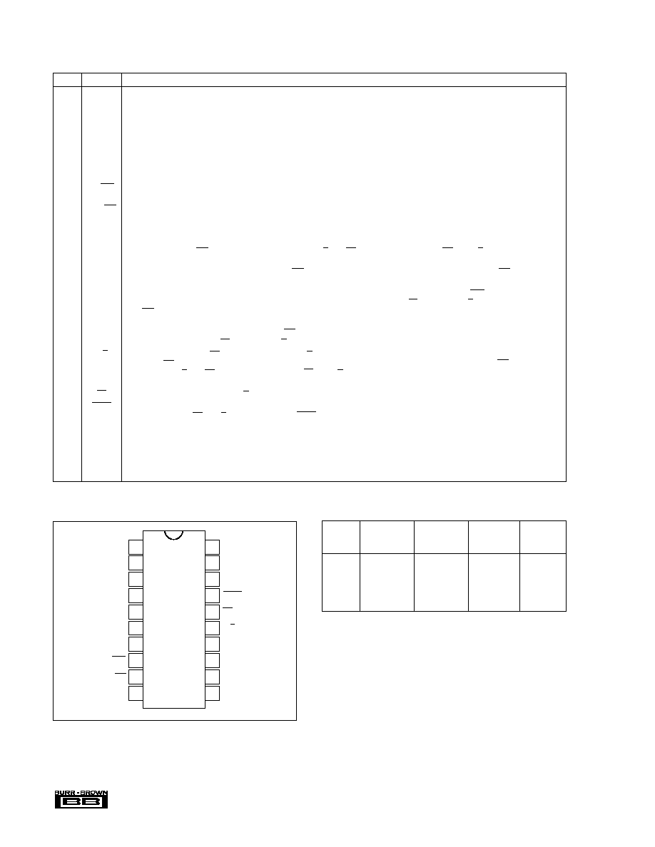
PIN #
NAME
DESCRIPTION
PIN ASSIGNMENTS
1
R1
IN
Analog Input. See Table I and Figure 4 for input range connections.
2
AGND1
Analog Ground. Used internally as ground reference point. Minimal current flow.
3
R2
IN
Analog Input. See Table I and Figure 4 for input range connections.
4
R3
IN
Analog Input. See Table I and Figure 4 for input range connections.
5
CAP
Reference Buffer Capacitor. 2.2
µ
F Tantalum to ground.
6
REF
Reference Input/Output. Outputs internal 2.5V reference. Can also be driven by external system reference. In both cases,
bypass to ground with a 2.2
µ
F Tantalum capacitor.
7
AGND2
Analog Ground.
8
SB/BTC
Select Straight Binary or Binary Two's Complement data output format. If HIGH, data will be output in a Straight Binary format. If
LOW, data will be output in a Binary Two's Complement format.
9
EXT/INT
Select External or Internal Clock for transmitting data. If HIGH, data will be output synchronized to the clock input on DATACLK. If
LOW, a convert command will initiate the transmission of the data from the previous conversion, along with 16 clock pulses output
on DATACLK.
10
DGND
Digital Ground.
11
SYNC
Synch Output. If EXT/INT is HIGH, either a rising edge on R/C with CS LOW or a falling edge on CS with R/C HIGH will output a
pulse on SYNC synchronized to the external DATACLK.
12
DATACLK
Either an input or an output depending on the EXT/INT level. Output data will be synchronized to this clock. If EXT/INT is LOW,
DATACLK will transmit 16 pulses after each conversion, and then remain LOW between conversions.
13
DATA
Serial Data Output. Data will be synchronized to DATACLK, with the format determined by the level of SB/BTC. In the external clock
mode, after 16 bits of data, the ADS7809 will output the level input on TAG as long as CS is LOW and R/C is HIGH (see Figure 3.) If
EXT/INT is LOW, data will be valid on both the rising and falling edges of DATACLK, and between conversions DATA will stay at the
level of the TAG input when the conversion was started.
14
TAG
Tag Input for use in external clock mode. If EXT/INT is HIGH, digital data input on TAG will be output on DATA with a delay of 16
DATACLK pulses as long as CS is LOW and R/C is HIGH. See Figure 3.
15
R/C
Read/Convert Input. With CS LOW, a falling edge on R/C puts the internal sample/hold into the hold state and starts a conversion.
When EXT/INT is LOW, this also initiates the transmission of the data results from the previous conversion. If EXT/INT is HIGH, a
rising edge on R/C with CS LOW, or a falling edge on CS with R/C HIGH, transmits a pulse on SYNC and initiates the transmission of
data from the previous conversion.
16
CS
Chip Select. Internally OR'ed with R/C.
17
BUSY
Busy Output. Falls when a conversion is started, and remains LOW until the conversion is completed and the data is latched into the
output shift register. CS or R/C must be HIGH when BUSY rises, or another conversion will start without time for signal acquisition.
18
PWRD
Power Down Input. If HIGH, conversions are inhibited and power consumption is significantly reduced. Results from the previous
conversion are maintained in the output shift register.
19
V
ANA
Analog Supply Input. Nominally +5V. Connect directly to pin 20, and decouple to ground with 0.1
µ
F ceramic and 10
µ
F Tantalum
capacitors.
20
V
DIG
Digital Supply Input. Nominally +5V. Connect directly to pin 19. Must be
V
ANA
.
PIN CONFIGURATION
V
DIG
V
ANA
PWRD
BUSY
CS
R/C
TAG
DATA
DATACLK
SYNC
R1
IN
AGND1
R2
IN
R3
IN
CAP
REF
AGND2
SB/BTC
EXT/INT
DGND
1
2
3
4
5
6
7
8
9
10
20
19
18
17
16
15
14
13
12
11
ADS7809
ANALOG
CONNECT R1
IN
CONNECT R2
IN
INPUT
VIA 200
VIA 100
CONNECT R3
IN
RANGE
TO
TO
TO
IMPEDANCE
±
10V
V
IN
AGND
CAP
22.9k
±
5V
AGND
V
IN
CAP
13.3k
±
3.33V
V
IN
V
IN
CAP
10.7k
0V to 10V
AGND
V
IN
AGND
13.3k
0V to 5V
AGND
AGND
V
IN
10.0k
0V to 4V
V
IN
AGND
V
IN
10.7k
TABLE I. Input Range Connections. See Figure 4 for
complete information.

Æ
ADS7809
5
FIGURE 1. Basic Conversion Timing.
MODE Acquire
t
4
t
5
t
1
t
3
t
7
t
6
Convert
Acquire
t
2
BUSY
CS, R/C
TABLE II. Conversion and Data Timing. T
A
= ≠40
∞
C to
+85
∞
C.
FIGURE 2. Serial Data Timing Using Internal Clock. (CS, EXT/INT and TAG Tied LOW.)
SYMBOL
DESCRIPTION
MIN
TYP MAX UNITS
t
1
Convert Pulse Width
40
6000
ns
t
2
BUSY Delay
65
ns
t
3
BUSY LOW
8
µ
s
t
4
BUSY Delay after
220
ns
End of Conversion
t
5
Aperture Delay
40
ns
t
6
Conversion Time
7.6
8
µ
s
t
7
Acquisition Time
2
µ
s
t
6
+ t
7
Throughput Time
9
10
µ
s
t
8
R/C LOW to DATACLK Delay
450
ns
t
9
DATACLK Period
440
ns
t
10
Data Valid to DATACLK
20
75
ns
HIGH Delay
t
11
Data Valid after
100
125
ns
DATACLK LOW Delay
t
12
External DATACLK
100
ns
t
13
External DATACLK HIGH
20
ns
t
14
External DATACLK LOW
30
ns
t
15
DATACLK HIGH
20
t
12
+5
ns
Setup Time
t
16
R/C to CS Setup Time
10
ns
t
17
SYNC Delay After
15
35
ns
DATACLK HIGH
t
18
Data Valid Delay
25
55
ns
t
19
CS to Rising Edge Delay
25
ns
t
20
Data Available after CS LOW
6
µ
s
1
MSB Valid
R/C
DATACLK
SDATA
t
8
t
11
t
10
t
9
2
3
15
16
Bit 14 Valid
Bit 1 Valid
Bit 13 Valid
LSB Valid
t
2
t
3
BUSY
t
1