Document Outline
- FEATURES
- APPLICATIONS
- DESCRIPTION
- ABSOLUTE MAXIMUM RATINGS(
- PACKAGE/ORDERING INFORMATION
- ELECTRICAL CHARACTERISTICS: +2.7V
- ELECTRICAL CHARACTERISTICS: +5V
- PIN CONFIGURATION
- PIN DESCRIPTIONS
- TIMING DIAGRAM
- TIMING CHARACTERISTICS
- TYPICAL CHARACTERISTICS
- THEORY OF OPERATION
- ANALOG INPUT
- REFERENCE INPUT
- DIGITAL INTERFACE
- ADDRESS BYTE
- COMMAND BYTE
- INITIATING CONVERSION
- READING DATA
- READING IN F/S MODE
- READING IN HS MODE
- TERMINATING A CONVERSION
- LAYOUT

12-Bit, Sampling A/D Converter
with I
2
C
TM
INTERFACE
FEATURES
q
50kHz SAMPLING RATE
q
NO MISSING CODES
q
2.7V TO 5V OPERATION
q
FOUR-WORD FILO
q
A0, A1 ADDRESS PINS
q
I
2
C INTERFACE SUPPORTS:
Standard, Fast, and High-Speed Modes
q
MSOP-8 PACKAGE
APPLICATIONS
q
VOLTAGE SUPPLY MONITORING
q
ISOLATED DATA ACQUISITION
q
TRANSDUCER INTERFACE
q
BATTERY-OPERATED SYSTEMS
q
REMOTE DATA ACQUISITION
DESCRIPTION
The ADS7823 is a single-supply, low-power, 12-bit data
acquisition device that features a serial I
2
C interface. The
Analog-to-Digital (A/D) converter features a sample-and-
hold amplifier and internal, asynchronous clock. The combi-
nation of an I
2
C serial two-wire interface and micropower
consumption makes the ADS7823 ideal for applications
requiring the A/D converter to be close to the input source in
remote locations and for applications requiring isolation. The
ADS7823 is available in an MSOP-8 package.
SAR
Serial
Interface
SDA
Comparator
S/H Amp
SCL
A0
A1
A
IN
V
REF
CDAC
ADS7823
SBAS180B � JUNE 2001 - REVISED SEPTEMBER 2003
www.ti.com
Copyright � 2001-2003, Texas Instruments Incorporated
Please be aware that an important notice concerning availability, standard warranty, and use in critical applications of
Texas Instruments semiconductor products and disclaimers thereto appears at the end of this data sheet.
PRODUCTION DATA information is current as of publication date.
Products conform to specifications per the terms of Texas Instruments
standard warranty. Production processing does not necessarily include
testing of all parameters.
All trademarks are the property of their respective owners.

ADS7823
2
SBAS180B
MAXIMUM
INTEGRAL
SPECIFIED
LINEARITY
TEMPERATURE
PACKAGE
PACKAGE
ORDERING
TRANSPORT
PRODUCT
ERROR (LSB)
RANGE
PACKAGE-LEAD
DESIGNATOR
(1)
MARKING
NUMBER
MEDIA, QUANTITY
ADS7823E
�
2
�40
�
C to +85
�
C
MSOP-8
DGK
B23
ADS7823E/250
Tape and Reel, 250
"
"
"
"
"
"
ADS7823E/2K5
Tape and Reel, 2500
ADS7823EB
�
1
�40
�
C to +85
�
C
MSOP-8
DGK
B23
ADS7823EB/250
Tape and Reel, 250
"
"
"
"
"
"
ADS7823EB/2K5
Tape and Reel, 2500
NOTE: (1) For the most current specifications and package information, refer to our web site at www.ti.com.
PACKAGE/ORDERING INFORMATION
ABSOLUTE MAXIMUM RATINGS
(1)
+V
DD
to GND ........................................................................ �0.3V to +6V
Digital Input Voltage to GND ................................. �0.3V to +V
DD
+ 0.3V
Analog Input Voltage to GND ........................................... �0.3V to +6.0V
Operating Temperature Range ........................................ �40
�
C to +85
�
C
Storage Temperature Range ......................................... �65
�
C to +150
�
C
Junction Temperature (T
J
max) .................................................... +150
�
C
TSSOP Package
Power Dissipation .................................................... (T
J
max � T
A
)/
JA
JA
Thermal Impedance ...................................................... +240
�
C/W
Lead Temperature, Soldering
Vapor Phase (60s) ............................................................ +215
�
C
Infrared (15s) ..................................................................... +220
�
C
NOTE: (1) Stresses above those listed under "Absolute Maximum Ratings"
may cause permanent damage to the device. Exposure to absolute maximum
conditions for extended periods may affect device reliability.
ELECTROSTATIC
DISCHARGE SENSITIVITY
This integrated circuit can be damaged by ESD. Texas Instru-
ments recommends that all integrated circuits be handled with
appropriate precautions. Failure to observe proper handling
and installation procedures can cause damage.
ESD damage can range from subtle performance degradation
to complete device failure. Precision integrated circuits may be
more susceptible to damage because very small parametric
changes could cause the device not to meet its published
specifications.
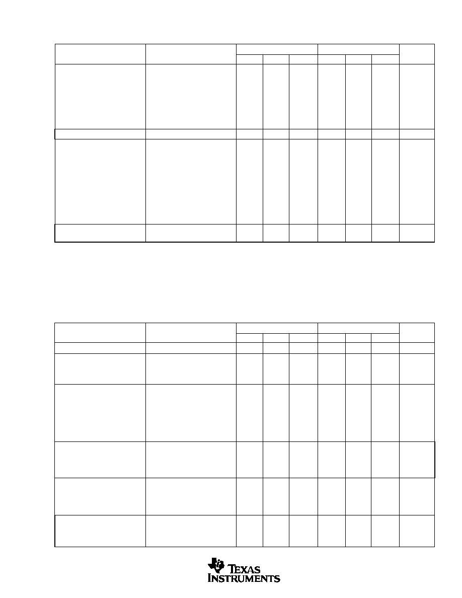
ELECTRICAL CHARACTERISTICS: +2.7V
At T
A
= �40
�
C to +85
�
C, +V
DD
= +2.7V, V
REF
= +2.5V, SCL Clock Frequency = 3.4MHz (High Speed Mode) unless otherwise noted.
ADS7823E
ADS7823EB
PARAMETER
CONDITIONS
MIN
TYP
MAX
MIN
TYP
MAX
UNITS
RESOLUTION
12
Bits
ANALOG INPUT
Full-Scale Input Range
0
V
REF
V
Input Capacitance
25
pF
Input Leakage Current
�
1
�
A
SYSTEM PERFORMANCE
No Missing Codes
12
Bits
Integral Linearity Error
�
1.0
�
2
�
0.5
�
1
LSB
(1)
Differential Linearity Error
�0.5, +1.0
�1.0, +3.0
�
0.5
LSB
Offset Error
�
1.0
�
4
�
0.75
�
3
LSB
Gain Error
�
1.0
�
4
�
0.75
�
3
LSB
Noise
33
�
Vrms
Power Supply Rejection
82
dB
SAMPLING DYNAMICS
Throughput Frequency
High Speed Mode: SCL = 3.4MHz
50
kHz
Fast Mode: SCL = 400kHz
8
kHz
Standard Mode, SCL = 100kHz
2
kHz
Conversion Time
8
�
s
AC ACCURACY
Total Harmonic Distortion
V
IN
= 2.5V
PP
at 10kHz
�82
dB
(2)
Signal-to-Ratio
V
IN
= 2.5V
PP
at 10kHz
72
dB
Signal-to-(Noise+Distortion) Ratio
V
IN
= 2.5V
PP
at 10kHz
71
dB
Spurious Free Dynamic Range
V
IN
= 2.5V
PP
at 10kHz
86
dB
VOLTAGE REFERENCE INPUT
Range
0.05
V
DD
V
Resistance
All Modes
1.0
G
Current Drain
At Code 800H, HS Mode: SCL = 3.4MHz
9.0
�
A
ADS7823
3
SBAS180B
DIGITAL INPUT/OUTPUT
Logic Family
CMOS
Logic Levels: V
IH
+V
DD
� 0.7
+V
DD
+ 0.5
V
V
IL
�0.3
+V
DD
� 0.3
V
V
OL
At min 3mA Sink Current
0.4
V
Input Leakage: I
IH
V
IH
= +V
DD
+0.5
10
�
A
I
IL
V
IL
= -0.3
-10
�
A
Data Format
Straight
Binary
ADS7823 HARDWARE ADDRESS
10010
Binary
POWER SUPPLY REQUIREMENTS
Power Supply Voltage, +V
DD
Specified Performance
2.7
3.6
V
Quiescent Current
High Speed Mode: SCL = 3.4MHz
250
370
�
A
Fast Mode: SCL = 400kHz
137
�
A
Standard Mode, SCL = 100kHz
109
�
A
Power Dissipation
High Speed Mode: SCL = 3.4MHz
680
1000
�
W
Fast Mode: SCL = 400kHz
370
�
W
Standard Mode, SCL = 100kHz
290
�
W
Powerdown Mode
High Speed Mode: SCL = 3.4MHz
60
�
A
w/Wrong Address Selected
Fast Mode: SCL = 400kHz
23
�
A
Standard Mode, SCL = 100kHz
5.4
�
A
Full Powerdown
SCL Pulled HIGH, SDA Pulled HIGH
2
3000
nA
TEMPERATURE RANGE
Specified Performance
�40
85
�
C
Specifications same as ADS7823E.
NOTES: (1) LSB means Least Significant Bit. With V
REF
equal to 2.5V, 1LSB is 610
�
V. (2) THD measured out to the 9th-harmonic.
ELECTRICAL CHARACTERISTICS: +2.7V
(Cont.)
At T
A
= �40
�
C to +85
�
C, +V
DD
= +2.7V, V
REF
= +2.5V, SCL Clock Frequency = 3.4MHz (High Speed Mode) unless otherwise noted.
ADS7823E
ADS7823EB
PARAMETER
CONDITIONS
MIN
TYP
MAX
MIN
TYP
MAX
UNITS
RESOLUTION
12
Bits
ANALOG INPUT
Full-Scale Input Range
0
V
REF
V
Input Capacitance
25
pF
Input Leakage Current
�
1
�
A
SYSTEM PERFORMANCE
No Missing Codes
12
Bits
Integral Linearity Error
�
1.0
�
2
�
0.5
�
1
LSB
(1)
Differential Linearity Error
�0.5, +1.0
�1, +3
�
0.5
LSB
Offset Error
�
1.0
�
4
�
0.75
�
3
LSB
Gain Error
�
1.0
�
4
�
0.75
�
3
LSB
Noise
33
�
Vrms
Power Supply Rejection
82
dB
SAMPLING DYNAMICS
Throughput Frequency
High Speed Mode: SCL = 3.4MHz
50
kHz
Fast Mode: SCL = 400kHz
8
kHz
Standard Mode, SCL = 100kHz
2
kHz
Conversion Time
8
�
s
AC ACCURACY
Total Harmonic Distortion
V
IN
= 2.5V
PP
at 10kHz
�82
dB
(2)
Signal-to-Ratio
V
IN
= 2.5V
PP
at 10kHz
72
dB
Signal-to-(Noise+Distortion) Ratio
V
IN
= 2.5V
PP
at 10kHz
71
dB
Spurious Free Dynamic Range
V
IN
= 2.5V
PP
at 10kHz
86
dB
VOLTAGE REFERENCE INPUT
Range
0.05
V
DD
V
Resistance
All Modes
1.0
G
Current Drain
At Code 800H, HS Mode: SCL = 3.4MHz
20
�
A
ELECTRICAL CHARACTERISTICS: +5V
At T
A
= �40
�
C to +85
�
C, +V
DD
= +5.0V, V
REF
= +5.0V, SCL Clock Frequency = 3.4MHz (High Speed Mode) unless otherwise noted.
ADS7823E
ADS7823EB
PARAMETER
CONDITIONS
MIN
TYP
MAX
MIN
TYP
MAX
UNITS

ADS7823
4
SBAS180B
DIGITAL INPUT/OUTPUT
Logic Family
CMOS
Logic Levels: V
IH
+V
DD
�
0.7
+V
DD
+ 0.5
V
V
IL
�0.3
+V
DD
�
0.3
V
V
OL
At min 3mA Sink Current
0.4
V
Input Leakage: I
IH
V
IH
= +V
DD
+0.5
10
�
A
I
IL
V
IL
= -0.3
-10
�
A
Data Format
Straight
Binary
ADS7823 HARDWARE ADDRESS
10010
Binary
POWER SUPPLY REQUIREMENTS
Power Supply Voltage, +V
DD
Specified Performance
4.75
5
5.25
V
Quiescent Current
High Speed Mode: SCL= 3.4MHz
0.72
1.0
mA
Fast Mode: SCL= 400kHz
380
�
A
Standard Mode, SCL=100kHz
240
�
A
Power Dissipation
High Speed Mode: SCL= 3.4MHz
3.6
5.0
mW
Fast Mode: SCL= 400kHz
1.9
mW
Standard Mode, SCL=100kHz
1.2
mW
Powerdown Mode
High Speed Mode: SCL= 3.4MHz
346
�
A
w/Wrong Address Selected
Fast Mode: SCL= 400kHz
136
�
A
Standard Mode, SCL=100kHz
34
�
A
Full Powerdown
SCL Pulled HIGH, SDA Pulled HIGH
3
3000
nA
TEMPERATURE RANGE
Specified Performance
�40
85
�
C
Specifications same as ADS7823E.
NOTES: (1) LSB means Least Significant Bit. With V
REF
equal to 2.5V, 1LSB is 610
�
V. (2) THD measured out to the 9th-harmonic.
PIN CONFIGURATION
Top View
MSOP
PIN DESCRIPTIONS
PIN
NAME
DESCRIPTION
1
V
REF
Reference Input, 2.5V Nominal
2
A
IN
Analog Input.
3
A0
Slave Address Bit 0
4
GND
Ground
5
A1
Slave Address Bit 1
6
SDA
Serial Data
7
SCL
Serial Clock
8
+V
DD
Power Supply, 3.3V Nominal
TIMING DIAGRAM
t
R
t
BUF
t
LOW
t
F
t
HD; STA
t
SP
t
HD; STA
t
SU; STA
t
HD; DAT
t
SU; DAT
t
HIGH
t
SU; STO
SCL
SDA
START
REPEATED
START
STOP
1
2
3
4
V
REF
A
IN
A0
GND
+V
DD
SCL
SDA
A1
8
7
6
5
ADS7823
ELECTRICAL CHARACTERISTICS: +5V
(Cont.)
At T
A
= �40
�
C to +85
�
C, +V
DD
= +5.0V, V
REF
= +5.0V, SCL Clock Frequency = 3.4MHz (High Speed Mode) unless otherwise noted.
ADS7823E
ADS7823EB
PARAMETER
CONDITIONS
MIN
TYP
MAX
MIN
TYP
MAX
UNITS
ADS7823
5
SBAS180B
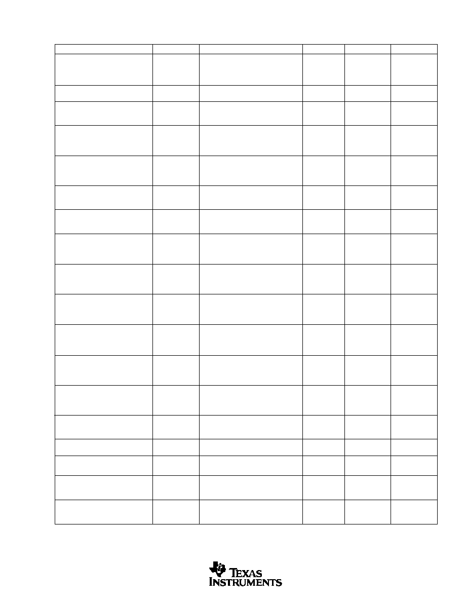
TIMING CHARACTERISTICS
(1)
At T
A
= �40
�
C to +85
�
C, +V
DD
= +2.7V, unless otherwise noted.
PARAMETER
SYMBOL
CONDITIONS
MIN
MAX
UNITS
SCL Clock Frequency
f
SCL
Standard Mode
100
kHz
Fast Mode
400
kHz
High-Speed Mode, C
B
= 100pF max
3.4
MHz
High-Speed Mode, C
B
= 400pF max
1.7
MHz
Bus Free Time Between a STOP and
t
BUF
Standard Mode
4.7
�
s
START Condition
Fast Mode
1.3
�
s
Hold Time (Repeated) START
t
HD
;
STA
Standard Mode
4.0
�
s
Condition
Fast Mode
600
ns
High-Speed Mode
160
ns
LOW Period of the SCL Clock
t
LOW
Standard Mode
4.7
�
s
Fast Mode
1.3
�
s
High-Speed Mode, C
B
= 100pF max
(2)
160
ns
High-Speed Mode, C
B
= 400pF max
(2)
320
ns
HIGH Period of the SCL Clock
t
HIGH
Standard Mode
4.0
�
s
Fast Mode
600
ns
High-Speed Mode, C
B
= 100pF max
(2)
60
ns
High-Speed Mode, C
B
= 400pF max
(2)
120
ns
Setup Time for a Repeated START
t
SU
;
STA
Standard Mode
4.7
�
s
Condition
Fast Mode
600
ns
High-Speed Mode
160
ns
Data Setup Time
t
SU
;
DAT
Standard Mode
250
ns
Fast Mode
100
ns
High-Speed Mode
10
ns
Data Hold Time
t
HD
;
DAT
Standard Mode
0
3.45
�
s
Fast Mode
0
0.9
�
s
High-Speed Mode, C
B
= 100pF max
(2)
0
(3)
70
ns
High-Speed Mode, C
B
= 400pF max
(2)
0
(3)
150
ns
Rise Time of SCL Signal
t
RCL
Standard Mode
1000
ns
Fast Mode
20 + 0.1C
B
300
ns
High-Speed Mode, C
B
= 100pF max
(2)
10
40
ns
High-Speed Mode, C
B
= 400pF max
(2)
20
80
ns
Rise Time of SCL Signal After a
t
RCL1
Standard Mode
1000
ns
Repeated START Condition and
Fast Mode
20 + 0.1C
B
300
ns
After an Acknowledge Bit
High-Speed Mode, C
B
= 100pF max
(2)
10
80
ns
High-Speed Mode, C
B
= 400pF max
(2)
20
160
ns
Fall Time of SCL Signal
t
FCL
Standard Mode
300
ns
Fast Mode
20 + 0.1C
B
300
ns
High-Speed Mode, C
B
= 100pF max
(2)
10
40
ns
High-Speed Mode, C
B
= 400pF max
(2)
20
80
ns
Rise Time of SDA Signal
t
RDA
Standard Mode
1000
ns
Fast Mode
20 + 0.1C
B
300
ns
High-Speed Mode, C
B
= 100pF max
(2)
10
80
ns
High-Speed Mode, C
B
= 400pF max
(2)
20
160
ns
Fall Time of SDA Signal
t
FDA
Standard Mode
300
ns
Fast Mode
20 + 0.1C
B
300
ns
High-Speed Mode, C
B
= 100pF max
(2)
10
80
ns
High-Speed Mode, C
B
= 400pF max
(2)
20
160
ns
Setup Time for STOP Condition
t
SU
;
STO
Standard Mode
4.0
�
s
Fast Mode
600
ns
High-Speed Mode
160
ns
Capacitive Load for SDA and SCL
C
B
400
pF
Line
Pulse Width of Spike Suppressed
t
SP
Fast Mode
50
ns
High-Speed Mode
10
ns
Noise Margin at the HIGH Level for
Standard Mode
Each Connected Device (Including
V
NH
Fast Mode
0.2V
DD
V
Hysteresis)
High-Speed Mode
Noise Margin at the LOW Level for
Standard Mode
Each Connected Device (Including
V
NL
Fast Mode
0.1V
DD
V
Hysteresis)
High-Speed Mode
NOTES: (1) All values referred to V
IHMIN
and V
ILMAX
levels. (2) For bus line loads C
B
between 100pF and 400pF the timing parameters must be linearly interpolated.
(3) A device must internally provide a data hold time to bridge the undefined part between V
IH
and V
IL
of the falling edge of the SCLH signal. An input circuit with
a threshold as low as possible for the falling edge of the SCLH signal minimizes this hold time.