 | –≠–ª–µ–∫—Ç—Ä–æ–Ω–Ω—ã–π –∫–æ–º–ø–æ–Ω–µ–Ω—Ç: ADS7824PB | –°–∫–∞—á–∞—Ç—å:  PDF PDF  ZIP ZIP |
1
Æ
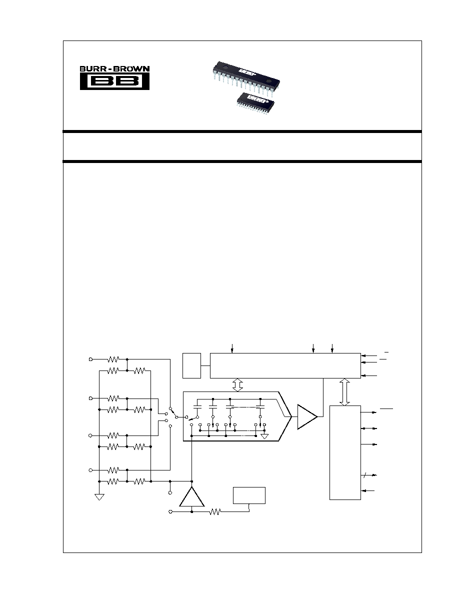
ADS7824
CDAC
6k
Internal
+2.5V Ref
Clock
BUSY
DATACLK
SDATA
D7-D0
BYTE
R/C
CS
PWRD
Successive Approximation Register
and Control Logic
Serial
Data
Out
or
Parallel
Data
Out
Comparator
Buffer
Continuous Conversion
Channel
REF
CAP
A0
CONTC
A1
40k
AIN
2
40k
AIN
1
40k
AIN
0
40k
AIN
3
20k
8k
20k
8k
20k
8k
20k
8k
8
4 Channel, 12-Bit Sampling CMOS A/D Converter
FEATURES
q
25
µ
s max SAMPLING AND CONVERSION
q
SINGLE +5V SUPPLY OPERATION
q
PIN-COMPATIBLE WITH 16-BIT ADS7825
q
PARALLEL AND SERIAL DATA OUTPUT
q
28-PIN 0.3" PLASTIC DIP AND SOIC
q
±
0.5 LSB max INL AND DNL
q
50mW max POWER DISSIPATION
q
50
µ
W POWER DOWN MODE
q
±
10V INPUT RANGE, FOUR CHANNEL
MULTIPLEXER
q
CONTINUOUS CONVERSION MODE
ADS7824
DESCRIPTION
The ADS7824 can acquire and convert 12 bits to
within
±
0.5 LSB in 25
µ
s max while consuming only
50mW max. Laser-trimmed scaling resistors provide
the standard industrial
±
10V input range and channel-
to-channel matching of
±
0.1%. The ADS7824 is a
low-power 12-bit sampling A/D with a four channel
input multiplexer, S/H, clock, reference, and a
parallel/serial microprocessor interface. It can be con-
figured in a continuous conversion mode to sequen-
tially digitize all four channels. The 28-pin ADS7824
is available in a plastic 0.3" DIP and in a SOIC, both
fully specified for operation over the industrial ≠40
∞
C
to +85
∞
C range.
Æ
International Airport Industrial Park ∑ Mailing Address: PO Box 11400, Tucson, AZ 85734 ∑ Street Address: 6730 S. Tucson Blvd., Tucson, AZ 85706 ∑ Tel: (520) 746-1111 ∑ Twx: 910-952-1111
Internet: http://www.burr-brown.com/ ∑ FAXLine: (800) 548-6133 (US/Canada Only) ∑ Cable: BBRCORP ∑ Telex: 066-6491 ∑ FAX: (520) 889-1510 ∑ Immediate Product Info: (800) 548-6132
ADS7824
ADS7824
www.burr-brown.com/databook/ADS7824.html
©
1996 Burr-Brown Corporation
PDS-1303B
Printed in U.S.A. October, 1997

2
Æ
ADS7824
SPECIFICATIONS
ELECTRICAL
At T
A
= ≠40
∞
C to +85
∞
C, f
S
= 40kHz, V
S1
= V
S2
= V
S
=
+5V
±
5%, using external reference, CONTC = 0V, unless otherwise specified.
ADS7824P, U
ADS7824PB, UB
PARAMETER
CONDITIONS
MIN
TYP
MAX
MIN
TYP
MAX
UNITS
The information provided herein is believed to be reliable; however, BURR-BROWN assumes no responsibility for inaccuracies or omissions. BURR-BROWN
assumes no responsibility for the use of this information, and all use of such information shall be entirely at the user's own risk. Prices and specifications are subject
to change without notice. No patent rights or licenses to any of the circuits described herein are implied or granted to any third party. BURR-BROWN does not
authorize or warrant any BURR-BROWN product for use in life support devices and/or systems.
RESOLUTION
12
T
(1)
Bits
ANALOG INPUT
Voltage Range
±
10V
T
V
Impedance
Channel On or Off
45.7
T
k
Capacitance
35
T
pF
THROUGHPUT SPEED
Conversion Time
20
T
µ
s
Acquisition Time
5
T
µ
s
Multiplexer Settling Time
Includes Acquisition
5
T
µ
s
Complete Cycle (Acquire and Convert)
25
T
µ
s
Complete Cycle (Acquire and Convert)
CONTC = +5V
40
T
µ
s
Throughput Rate
40
T
kHz
DC ACCURACY
Integral Linearity Error
±
0.15
±
1
T
±
0.5
LSB
(2)
Differential Linearity Error
±
0.15
±
1
T
±
0.5
LSB
No Missing Codes
Guaranteed
T
Transition Noise
(3)
0.1
T
LSB
Full Scale Error
(4)
Internal Reference
±
0.5
±
0.25
%
Full Scale Error Drift
Internal Reference
±
7
±
5
ppm/
∞
C
Full Scale Error
(4)
±
0.5
±
0.25
%
Full Scale Error Drift
±
2
T
ppm/
∞
C
Bipolar Zero Error
±
10
T
mV
Bipolar Zero Error Drift
±
2
T
ppm/
∞
C
Channel-to-Channel Mismatch
±
0.1
±
0.1
%
Power Supply Sensitivity
+4.75 < V
S
< +5.25
±
0.5
T
LSB
AC ACCURACY
Spurious-Free Dynamic Range
(5)
f
IN
= 1kHz
80
90
T
T
dB
Total Harmonic Distortion
f
IN
= 1kHz
≠90
≠80
T
T
dB
Signal-to-(Noise+Distortion)
f
IN
= 1kHz
70
73
72
T
dB
Signal-to-Noise
f
IN
= 1kHz
70
73
72
T
dB
Channel Separation
(6)
f
IN
= 1kHz
90
100
T
T
dB
≠3dB Bandwidth
2
T
MHz
Useable Bandwidth
(7)
90
T
kHz
SAMPLING DYNAMICS
Aperture Delay
40
T
ns
Transient Response
(8)
FS Step
5
T
µ
s
Overvoltage Recovery
(9)
1
T
µ
s
REFERENCE
Internal Reference Voltage
2.48
2.5
2.52
T
T
T
V
Internal Reference Source Current
1
T
µ
A
(Must use external buffer)
External Reference Voltage Range
2.3
2.5
2.7
T
T
T
V
for Specified Linearity
External Reference Current Drain
V
REF
= +2.5V
100
T
µ
A
DIGITAL INPUTS
Logic Levels
V
IL
≠0.3
+0.8
T
T
V
V
IH
+2.4
V
S
+0.3V
T
T
V
I
IL
±
10
T
µ
A
I
IH
±
10
T
µ
A
DIGITAL OUTPUTS
Data Format
Parallel in two bytes; Serial
T
Data Coding
Binary Two's Complement
T
V
OL
I
SINK
= 1.6mA
+0.4
T
V
V
OH
I
SOURCE
= 500
µ
A
+4
T
V
Leakage Current
High-Z State, V
OUT
= 0V to V
S
±
5
T
µ
A
Output Capacitance
High-Z State
15
T
pF

3
Æ
ADS7824
SPECIFICATIONS
(CONT)
ELECTRICAL
At T
A
= ≠40
∞
C to +85
∞
C, f
S
= 40kHz, V
S1
= V
S2
= V
S
=
+5V
±
5%, using external reference, CONTC = 0V, unless otherwise specified.
ADS7824P, U
ADS7824PB, UB
PARAMETER
CONDITIONS
MIN
TYP
MAX
MIN
TYP
MAX
UNITS
DIGITAL TIMING
Bus Access Time
PAR/SER = +5V
83
T
ns
Bus Relinquish Time
PAR/SER = +5V
83
T
ns
Data Clock
PAR/SER = 0V
Internal Clock (Output only when
EXT/INT LOW
0.5
1.5
T
T
MHz
transmitting data)
External Clock
EXT/INT HIGH
0.1
10
T
T
MHz
POWER SUPPLIES
V
S1
= V
S2
= V
S
+4.75
+5
+5.25
T
T
T
V
Power Dissipation
f
S
= 40kHz
50
T
mW
PWRD HIGH
50
T
µ
W
TEMPERATURE RANGE
Specified Performance
≠40
+85
T
T
∞
C
Storage
≠65
+150
T
T
∞
C
Thermal Resistance (
JA
)
Plastic DIP
75
T
∞
C/W
SOIC
75
T
∞
C/W
NOTES: (1) An asterik (
T
) specifies same value as grade to the left. (2) LSB means Least Significant Bit. For the 12-bit,
±
10V input ADS7824, one LSB is 4.88mV. (3)
Typical rms noise at worst case transitions and temperatures. (4) Full scale error is the worst case of ≠Full Scale or +Full Scale untrimmed deviation from ideal first and
last code transitions, divided by the transition voltage (not divided by the full-scale range) and includes the effect of offset error. (5) All specifications in dB are referred
to a full-scale
±
10V input. (6) A full scale sinewave input on one channel will be attenuated by this amount on the other channels. (7) Useable Bandwidth defined as
Full-Scale input frequency at which Signal-to-(Noise+Distortion) degrades to 60dB, or 10 bits of accuracy. (8) The ADS7824 will accurately acquire any input step if given
a full acquisition period after the step. (9) Recovers to specified performance after 2 x FS input overvoltage, and normal acquisitions can begin.
PIN CONFIGURATION
ELECTROSTATIC
DISCHARGE SENSITIVITY
This integrated circuit can be damaged by ESD. Burr-Brown
recommends that all integrated circuits be handled with
appropriate precautions. Failure to observe proper handling
and installation procedures can cause damage.
ESD damage can range from subtle performance degrada-
tion to complete device failure. Precision integrated circuits
may be more susceptible to damage because very small
parametric changes could cause the device not to meet its
published specifications.
ABSOLUTE MAXIMUM RATINGS
Analog Inputs: AIN
0
, AIN
1
, AIN
2
, AIN
3
..............................................
±
15V
REF ................................... (AGND2 ≠0.3V) to (V
S
+ 0.3V)
CAP ........................................ Indefinite Short to AGND2,
Momentary Short to V
S
V
S1
and V
S2
to AGND2 ........................................................................... 7V
V
S1
to V
S2
..........................................................................................
±
0.3V
Difference between AGND1, AGND2 and DGND .............................
±
0.3V
Digital Inputs and Outputs .......................................... ≠0.3V to (V
S
+ 0.3V)
Maximum Junction Temperature ..................................................... 150
∞
C
Internal Power Dissipation ............................................................. 825mW
Lead Temperature (soldering, 10s) ................................................ +300
∞
C
Maximum Input Current to Any Pin ................................................. 100mA
PACKAGE
MINIMUM SIGNAL-
DRAWING
TEMPERATURE
MAXIMUM INTEGRAL
TO-(NOISE + DISTORTION)
PRODUCT
PACKAGE
NUMBER
(1)
RANGE
LINEARITY ERROR (LSB)
RATIO (dB)
ADS7824P
Plastic Dip
246
≠40
∞
C to +85
∞
C
±
1
70
ADS7824PB
Plastic Dip
246
≠40
∞
C to +85
∞
C
±
0.5
72
ADS7824U
SOIC
217
≠40
∞
C to +85
∞
C
±
1
70
ADS7824UB
SOIC
217
≠40
∞
C to +85
∞
C
±
0.5
72
NOTE: (1) For detailed drawing and dimension table, please see end of data sheet, or Appendix C of Burr-Brown IC Data Book.
PACKAGE/ORDERING INFORMATION
Top View
DIP/SOIC
V
S1
V
S2
PWRD
CONTC
BUSY
CS
R/C
BYTE
PAR/SER
A0
A1
D0
D1
D2
AGND1
AIN
0
AIN
1
AIN
2
AIN
3
CAP
REF
AGND2
D7
D6
D5
D4
D3
DGND
1
2
3
4
5
6
7
8
9
10
11
12
13
14
28
27
26
25
24
23
22
21
20
19
18
17
16
15
ADS7824
TRI-STATE
TRI-STATE
TRI-STATE
EXT/INT
SYNC
TAG
SDATA
DATACLK

4
Æ
ADS7824
1
AGND1
Analog Ground. Used internally as ground reference point.
2
AIN
0
Analog Input Channel 0. Full-scale input range is
±
10V.
3
AIN
1
Analog Input Channel 1. Full-scale input range is
±
10V.
4
AIN
2
Analog Input Channel 2. Full-scale input range is
±
10V.
5
AIN
3
Analog Input Channel 3. Full-scale input range is
±
10V.
6
CAP
Internal Reference Output Buffer. 2.2
µ
F Tantalum to ground.
7
REF
Reference Input/Output. Outputs +2.5V nominal. If used externally, must be buffered to maintain ADS7825 accuracy.
Can also be driven by external system reference. In both cases, bypass to ground with a 2.2
µ
F Tantalum capacitor.
8
AGND2
Analog Ground.
9
D7
O
Parallel Data Bit 7 if PAR/SER HIGH; Tri-state if PAR/SER LOW. See Table I.
10
D6
O
Parallel Data Bit 6 if PAR/SER HIGH; Tri-state if PAR/SER LOW. See Table I.
11
D5
O
Parallel Data Bit 5 if PAR/SER HIGH; Tri-state if PAR/SER LOW. See Table I.
12
D4
I/O
Parallel Data Bit 4 if PAR/SER HIGH; if PAR/SER LOW, a LOW level input here will transmit serial data on SDATA from
the previous conversion using the internal serial clock; a HIGH input here will transmit serial data using an external serial
clock input on DATACLK (D2). See Table I.
13
D3
O
Parallel Data Bit 3 if PAR/SER HIGH; SYNC output if PAR/SER LOW. See Table I.
14
DGND
Digital Ground.
15
D2
I/O
Parallel Data Bit 2 if PAR/SER HIGH; if PAR/SER LOW, this will output the internal serial clock if EXT/INT (D4) is LOW;
will be an input for an external serial clock if EXT/INT (D4) is HIGH. See Table I.
16
D1
O
Parallel Data Bit 1 if PAR/SER HIGH; SDATA serial data output if PAR/SER LOW. See Table I.
17
D0
I/O
Parallel Data Bit 0 if PAR/SER HIGH; TAG data input if PAR/SER LOW. See Table I.
18
A1
I/O
Channel Address. Input if CONTC LOW, output if CONTC HIGH. See Table I.
19
A0
I/O
Channel Address. Input if CONTC LOW, output if CONTC HIGH. See Table I.
20
PAR/SER
I
Select Parallel or Serial Output. If HIGH, parallel data will be output on D0 thru D7. If LOW, serial data will be output on
SDATA. See Table I and Figure 1.
21
BYTE
I
Byte Select. Only used with parallel data, when PAR/SER HIGH. Determines which byte is available on D0 thru D7.
Changing BYTE with CS LOW and R/C HIGH will cause the data bus to change accordingly. LOW selects the 8 MSBs;
HIGH selects the 4 LSBs, see Figures 2 and 3.
22
R/C
I
Read/Convert Input. With CS LOW, a falling edge on R/C puts the internal sample/hold into the hold state and starts a
conversion. With CS LOW, a rising edge on R/C enables the output data bits if PAR/SER HIGH, or starts transmission
of serial data if PAR/SER LOW and EXT/INT HIGH.
23
CS
I
Chip Select. Internally OR'd with R/C. With CONTC LOW and R/C LOW, a falling edge on CS will initiate a conversion.
With R/C HIGH, a falling edge on CS will enable the output data bits if PAR/SER HIGH, or starts transmission of serial
data if PAR/SER LOW and EXT/INT HIGH.
24
BUSY
O
Busy Output. Falls when conversion is started; remains LOW until the conversion is completed and the data is latched
into the output register. In parallel output mode, output data will be valid when BUSY rises, so that the rising edge can
be used to latch the data.
25
CONTC
I
Continuous Conversion Input. If LOW, conversions will occur normally when initiated using CS and R/C; if HIGH,
acquisition and conversions will take place continually, cycling through all four input channels, as long as CS, R/C and
PWRD are LOW. See Table I. For serial mode only.
26
PWRD
I
Power Down Input. If HIGH, conversions are inhibited and power consumption is significantly reduced. Results from the
previous conversion are maintained in the output register. In the continuous conversion mode, the multiplexer address
channel is reset to channel 0
27
V
S2
Supply Input. Nominally +5V. Connect directly to pin 28. Decouple to ground with 0.1
µ
F ceramic and 10
µ
F Tantalum
capacitors.
28
V
S1
Supply Input. Nominally +5V. Connect directly to pin 27.
PIN #
NAME
I/O
DESCRIPTION
PIN ASSIGNMENTS

5
Æ
ADS7824
0.2
0
≠0.2
≠25
≠50
0
25
50
75
100
0.2
0
≠0.2
2
1
0
≠1
≠2
BPZ Error
+FS Error
≠FS Error
ENDPOINT ERRORS
Temperature (∞C)
mV From Ideal
Percent
From Ideal
Percent
From Ideal
ADJACENT CHANNEL CROSSTALK, WORST PAIR
(8192 Point FFT; AIN
3
= 10.1kHz, ≠0.1dB; AIN
2
= AGND)
0
≠10.0
≠20.0
≠30.0
≠40.0
≠50.0
≠60.0
≠70.0
≠80.0
≠90.0
≠100.0
≠110.0
0
5
10
15
20
Amplitude (dB)
Frequency (kHz)
TYPICAL PERFORMANCE CURVES
At T
A
= +25
∞
C, f
S
= 40kHz, V
S1
= V
S2
= +5V, using internal reference, unless otherwise noted.
FREQUENCY SPECTRUM
(8192 Point FFT; f
IN
= 1.02kHz, ≠0.5dB)
0
≠10.0
≠20.0
≠30.0
≠40.0
≠50.0
≠60.0
≠70.0
≠80.0
≠90.0
≠100.0
≠110.0
0
5
10
15
20
Amplitude (dB)
Frequency (kHz)
ADJACENT CHANNEL CROSSTALK, WORST PAIR
(8192 Point FFT; AIN
3
= 1.02kHz, ≠0.1dB; AIN
2
= AGND)
0
≠10.0
≠20.0
≠30.0
≠40.0
≠50.0
≠60.0
≠70.0
≠80.0
≠90.0
≠100.0
≠110.0
0
5
10
15
20
Amplitude (dB)
Frequency (kHz)
POWER SUPPLY RIPPLE SENSITIVITY
INL/DNL DEGRADATION PER LSB OF P-P RIPPLE
Power Supply Ripple Frequency (Hz)
10
1
10
2
10
3
10
4
10
5
10
6
10
7
1
10
≠1
10
≠2
10
≠3
10
≠4
10
≠5
Linearity Degradation (LSB/LSB)
INL
DNL
0.3
0.2
0.1
0
≠0.1
≠0.2
≠0.3
0
512
1024
1536
2048
2560
3072
3584
4095
Decimal Code
12-Bit LSBs
0.3
0.2
0.1
0
≠0.1
≠0.2
≠0.3
12-Bit LSBs
0
512
1024
1536
2048
2560
3072
3584
4095
Decimal Code
All Codes INL
All Codes DNL