 | ÐлекÑÑоннÑй компоненÑ: ADS831 | СкаÑаÑÑ:  PDF PDF  ZIP ZIP |
Äîêóìåíòàöèÿ è îïèñàíèÿ www.docs.chipfind.ru
8-Bit, 80MHz Sampling
ANALOG-TO-DIGITAL CONVERTER
FEATURES
q
HIGH SNR: 49dB
q
INTERNAL / EXTERNAL REFERENCE
OPTION
q
SINGLE-ENDED OR
DIFFERENTIAL ANALOG INPUT
q
PROGRAMMABLE INPUT RANGE:
1Vp-p /2Vp-p
q
LOW POWER: 275mW
q
LOW DNL: 0.35LSB
q
SINGLE +5V SUPPLY OPERATION
q
20-PIN SSOP PACKAGE
APPLICATIONS
q
MEDICAL IMAGING
q
VIDEO DIGITIZING
q
COMPUTER SCANNERS
q
COMMUNICATIONS
q
DISK-DRIVE CONTROL
DESCRIPTION
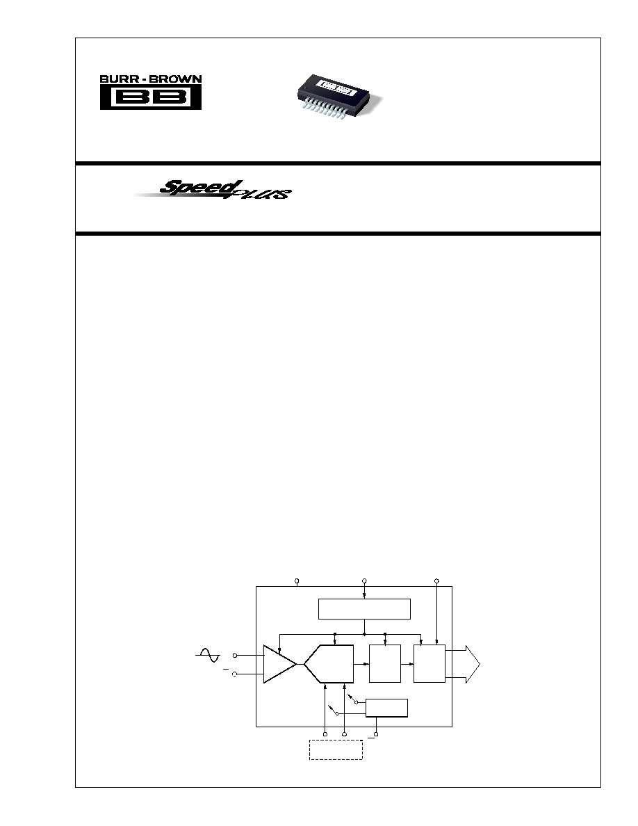
The ADS831 is a pipeline, CMOS analog-to-digital con-
verter that operates from a single +5V power supply. This
converter provides excellent performance with a single-
ended input and can be operated with a differential input
for added spurious performance. This high performance
converter includes an 8-bit quantizer, high bandwidth
track/hold, and a high accuracy internal reference. It also
allows for the user to disable the internal reference and
utilize external references. This external reference option
provides excellent gain and offset matching when used in
multi-channel applications or in applications where DC full
scale range adjustment is required.
The ADS831 employs digital error correction techniques to
provide excellent differential linearity for demanding im-
aging applications. Its low distortion and high SNR give
the extra margin needed for medical imaging, communica-
tions, video, and test instrumentation.
The ADS831 is specified at a maximum sampling fre-
quency of 80MHz and a single-ended input range of 1.5V
to 3.5V. The ADS831 is available in a 20-lead SSOP
package and is pin-for-pin compatible with the 8-bit, 60MHz
ADS830.
TM
ADS831
®
¤
ADS831
International Airport Industrial Park · Mailing Address: PO Box 11400, Tucson, AZ 85734 · Street Address: 6730 S. Tucson Blvd., Tucson, AZ 85706 · Tel: (520) 746-1111
Twx: 910-952-1111 · Internet: http://www.burr-brown.com/ · Cable: BBRCORP · Telex: 066-6491 · FAX: (520) 889-1510 · Immediate Product Info: (800) 548-6132
©
1998 Burr-Brown Corporation
PDS-1430B
Printed in U.S.A. October, 1998
8-Bit
Pipelined
A/D Core
Internal
Reference
Optional External
Reference
Timing
Circuitry
Error
Correction
Logic
3-State
Outputs
T/H
CLK
VDRV
ADS831
+V
S
Int/Ext
D0
D7
·
·
·
IN
V
IN
IN
(Opt)
®
ADS831
2
SPECIFICATIONS
At T
A
= full specified temperature range, single-ended input range = 1.5V to 3.5V, sampling rate = 80MHz, and external reference, unless otherwise noted.
ADS831E
PARAMETER
CONDITIONS
MIN
TYP
MAX
UNITS
RESOLUTION
8 Guaranteed
Bits
SPECIFIED TEMPERATURE RANGE
Ambient Air
40 to +85
°
C
ANALOG INPUT
Standard Single-Ended Input Range
2Vp-p
1.5
3.5
V
Optional Single-Ended Input Range
1Vp-p
2
3
V
Common-Mode Voltage
2.5
V
Optional Differential Input Range
2Vp-p
2
3
V
Analog Input Bias Current
1
µ
A
Input Impedance
1.25 || 5
M
|| pF
Track-Mode Input Bandwidth
3dBFS
300
MHz
CONVERSION CHARACTERISTICS
Sample Rate
10k
80M
Samples/s
Data Latency
4
Clk Cyc
DYNAMIC CHARACTERISTICS
Differential Linearity Error (largest code error)
f = 1MHz
±
0.25
±
1.0
LSB
f = 10MHz
±
0.35
LSB
No Missing Codes
Guaranteed
Integral Nonlinearity Error, f = 1MHz
±
0.5
±
2.0
LSBs
Spurious Free Dynamic Range
(1)
f = 1MHz (1dB input)
67
dBFS
(2)
f = 10MHz (1dB input)
50
65
dBFS
Two-Tone Intermodulation Distortion
(3)
f = 9.5MHz and 9.9MHz (7dB each tone)
57
dBc
Signal-to-Noise Ratio (SNR)
Referred to Full Scale
f = 1MHz
49
dB
f = 10MHz
46
49
dB
Signal-to-(Noise + Distortion) (SINAD)
Referred to Full Scale
f = 1MHz
48.5
dB
f = 10MHz
44
48.5
dB
Effective Number of Bits
(4)
, f = 1MHz
7.8
Bits
Output Noise
Input Tied to Common-Mode
0.2
LSBs rms
Aperture Delay Time
3
ns
Aperture Jitter
1.2
ps rms
Overvoltage Recovery Time
2
ns
Full-Scale Step Acquisition Time
2.5
ns
DIGITAL INPUTS
Logic Family
Convert Command
Start Conversion
High Level Input Current
(5)
(V
IN
= 5V)
100
µ
A
Low Level Input Current (V
IN
= 0V)
10
µ
A
High Level Input Voltage
+3.5
V
Low Level Input Voltage
+1.0
V
Input Capacitance
5
pF
DIGITAL OUTPUTS
Logic Family
Logic Coding
Low Output Voltage (I
OL
= 50
µ
A)
VDRV = 5V
+0.1
V
Low Output Voltage, (I
OL
= 1.6mA)
+0.2
V
High Output Voltage, (I
OH
= 50
µ
A)
+4.9
V
High Output Voltage, (I
OH
= 0.5mA)
+4.8
V
Low Output Voltage, (I
OL
= 50
µ
A)
VDRV = 3V
+0.1
V
High Output Voltage, (I
OH
= 50
µ
A)
+2.8
V
Output Capacitance
5
pF
ACCURACY (Internal Reference, 2Vp-p, Unless Otherwise Noted)
Zero Error (Referred to FS)
at 25
°
C
2.5
±
0.5
+2.5
%FS
Zero Error Drift (Referred to FS)
±
53
ppm/
°
C
Gain Error
(6)
at 25
°
C
2.5
±
0.5
+2.5
%FS
Gain Error Drift
(6)
±
75
ppm/
°
C
Power Supply Rejection of Gain
V
S
=
±
5%
55
dB
Internal REFT Tolerance
Deviation from Ideal 3.0V
±
10
±
100
mV
Internal REFB Tolerance
Deviation from Ideal 2.0V
±
10
±
100
mV
External REFT Voltage Range
REFB + 0.8
3.0
V
S
1.25
V
External REFB Voltage Range
1.25
2.0
REFT 0.8
V
Reference Input Resistance
REFT to REFB
800
CMOS Compatible
Rising Edge of Convert Clock
CMOS/TTL Compatible
Straight Offset Binary
3
ADS831
®
GND
Bit 1 (MSB)
Bit 2
Bit 3
Bit 4
Bit 5
Bit 6
Bit 7
Bit 8 (LSB)
CLK
VDRV
+V
S
GND
IN
IN
CM
REFT
REFB
INT/EXT
RSEL
1
2
3
4
5
6
7
8
9
10
20
19
18
17
16
15
14
13
12
11
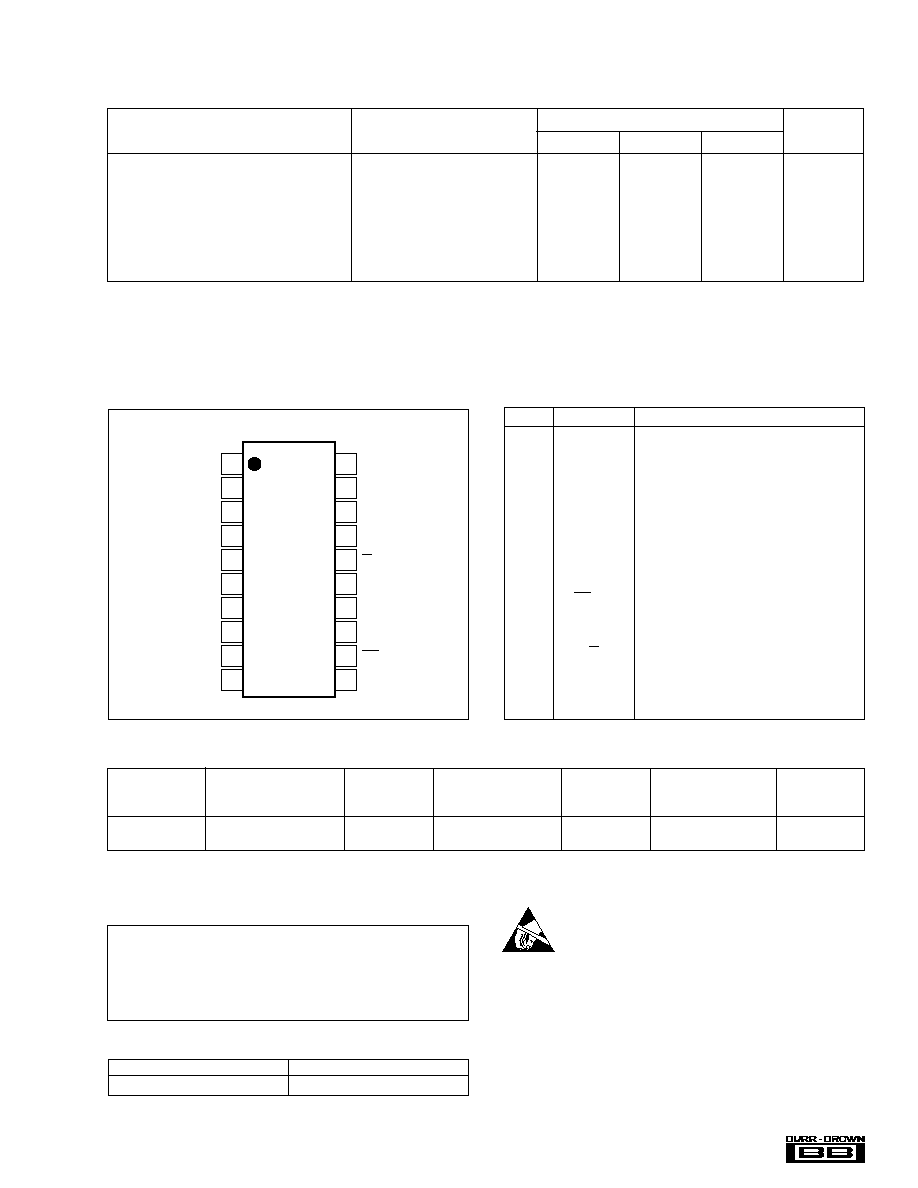
ADS831
POWER SUPPLY REQUIREMENTS
Supply Voltage: +V
S
Operating
+4.75
+5.0
+5.25
V
Supply Current: +I
S
Operating
58
70
mA
Power Dissipation: VDRV = 5V
External Reference
290
350
mW
VDRV = 3V
External Reference
275
mW
VDRV = 5V
Internal Reference
310
mW
VDRV = 3V
Internal Reference
285
mW
Thermal Resistance,
JA
20-Lead SSOP
115
°
C/W
NOTES: (1) Spurious Free Dynamic Range refers to the magnitude of the largest harmonic. (2) dBFS means dB relative to Full Scale. (3) Two-tone
intermodulation distortion is referred to the largest fundamental tone. This number will be 6dB higher if it is referred to the magnitude of the two-tone fundamental
envelope. (4) Effective number of bits (ENOB) is defined by (SINAD 1.76 ) /6.02. (5) A 50k
pull-down resistor is inserted internally. (6) Excludes internal
reference.
SPECIFICATIONS
At T
A
= full specified temperature range, single-ended input range = 1.5V to 3.5V, sampling rate = 80MHz, and external reference, unless otherwise noted.
ADS831E
PARAMETER
CONDITIONS
MIN
TYP
MAX
UNITS
PIN
DESIGNATOR
DESCRIPTION
1
GND
Ground
2
Bit 1
Data Bit 1 (D7) (MSB)
3
Bit 2
Data Bit 2 (D6)
4
Bit 3
Data Bit 3 (D5)
5
Bit 4
Data Bit 4 (D4)
6
Bit 5
Data Bit 5 (D3)
7
Bit 6
Data Bit 6 (D2)
8
Bit 7
Data Bit 7 (D1)
9
Bit 8
Data Bit 8 (D0) (LSB)
10
CLK
Convert Clock
11
RSEL
Input Range Select: HI = 2V; LO = 1V
12
INT/EXT
Reference Select: HI = External; LO = Internal
13
REFB
Bottom Reference
14
REFT
Top Reference
15
CM
Common-Mode Voltage Output
16
IN
Complementary Input
17
IN
Analog Input
18
GND
Ground
19
+V
S
+5V Supply
20
VDRV
Output Logic Driver Supply Voltage
PIN DESCRIPTIONS
PIN CONFIGURATION
Top View
SSOP
PACKAGE
SPECIFIED
DRAWING
TEMPERATURE
PACKAGE
ORDERING
TRANSPORT
PRODUCT
PACKAGE
NUMBER
(1)
RANGE
MARKING
NUMBER
MEDIA
ADS831E
20-Lead SSOP (QSOP)
349
40
°
C to +85
°
C
ADS831E
ADS831E
Rails
"
"
"
"
"
ADS831E/1K
Tape and Reel
NOTES: (1) For detailed drawing and dimension table, please see end of data sheet, or Appendix C of Burr-Brown IC Data Book. For detailed Tape and Reel
mechanical information, refer to Appendix B of Burr-Brown IC Data Book.
PACKAGE/ORDERING INFORMATION
ELECTROSTATIC
DISCHARGE SENSITIVITY
This integrated circuit can be damaged by ESD. Burr-Brown recom-
mends that all integrated circuits be handled with
appropriate precautions. Failure to observe proper handling and
installation procedures can cause damage.
ESD damage can range from subtle performance degradation to
complete device failure. Precision integrated circuits may be more
susceptible to damage because very small parametric changes could
cause the device not to meet its published specifications.
PRODUCT
DEMO BOARD
ADS831
DEM-ADS831E
DEMO BOARD ORDERING INFORMATION
+V
S
....................................................................................................... +6V
Analog Input ............................................................. 0.3V to (+V
S
+ 0.3V)
Logic Input ............................................................... 0.3V to (+V
S
+ 0.3V)
Case Temperature ......................................................................... +100
°
C
Junction Temperature .................................................................... +150
°
C
Storage Temperature ..................................................................... +150
°
C
ABSOLUTE MAXIMUM RATINGS
®
ADS831
4
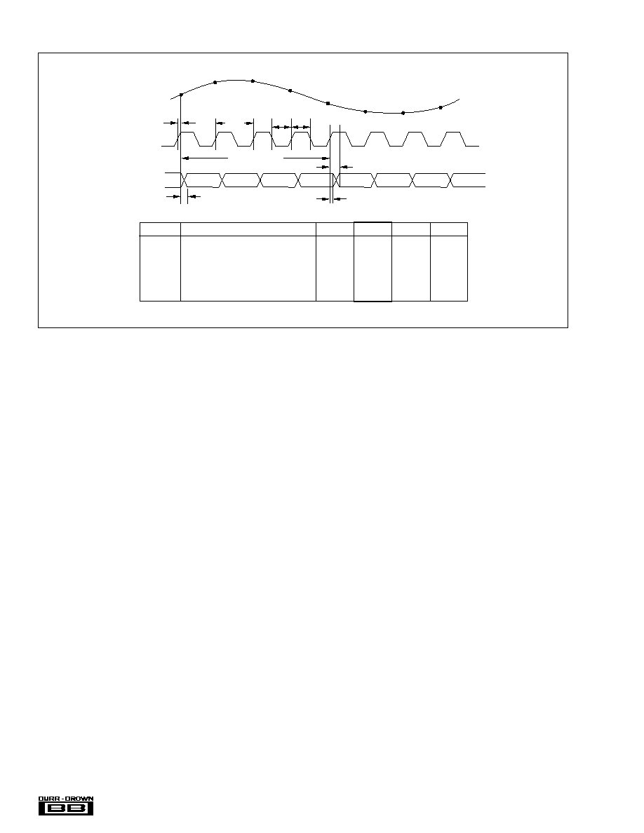
TIMING DIAGRAM
SYMBOL
DESCRIPTION
MIN
TYP
MAX
UNITS
t
CONV
Convert Clock Period
12.5
100
µ
s
ns
t
L
Clock Pulse Low
5.8
6.25
ns
t
H
Clock Pulse High
5.8
6.25
ns
t
D
Aperture Delay
3
ns
t
1
Data Hold Time, C
L
= 0pF
3.9
ns
t
2
New Data Delay Time, C
L
= 15pF max
5.9
12
ns
The information provided herein is believed to be reliable; however, BURR-BROWN assumes no responsibility for inaccuracies or omissions. BURR-BROWN assumes no responsibility
for the use of this information, and all use of such information shall be entirely at the user's own risk. Prices and specifications are subject to change without notice. No patent rights
or licenses to any of the circuits described herein are implied or granted to any third party. BURR-BROWN does not authorize or warrant any BURR-BROWN product for use in life
support devices and/or systems.
4 Clock Cycles
Data Invalid
t
D
t
L
t
H
t
CONV
N4
N3
N2
N1
N
N+1
N+2
N+3
Data Out
Clock
Analog In
N
t
2
N+1
N+2
N+3
N+4
N+5
N+6
N+7
t
1
5
ADS831
®
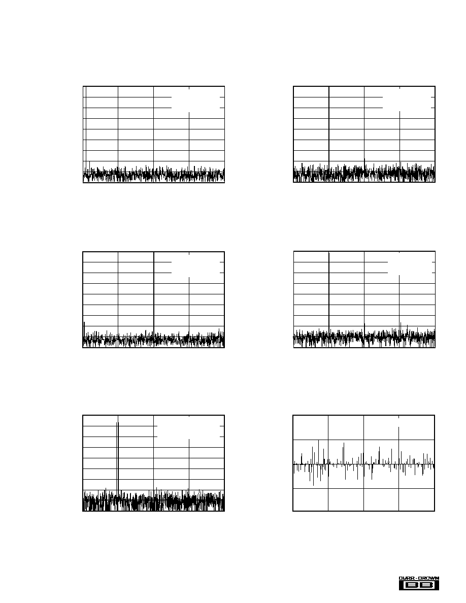
SPECTRAL PERFORMANCE
Frequency (MHz)
0
10
20
30
40
f
IN
= 20MHz
SNR = 49dBFS
SFDR = 66dBFS
Magnitude (dB)
0
10
20
30
40
50
60
70
80
90
SPECTRAL PERFORMANCE
Frequency (MHz)
0
10
20
30
40
Magnitude (dB)
0
10
20
30
40
50
60
70
80
90
f
IN
= 10MHz
SNR = 49dBFS
SFDR = 67dBFS
SPECTRAL PERFORMANCE
Frequency (MHz)
Magnitude (dB)
0
10
20
30
40
0
10
20
30
40
50
60
70
80
90
f
IN
= 1MHz
SNR = 49dBFS
SFDR = 68dBFS
TWO-TONE INTERMODULATION DISTORTION
Frequency (MHz)
Magnitude (dBFSR)
0
10
20
30
40
50
60
70
80
90
0
10
20
30
40
f
1
= 9.5MHz at 7dBFS
f
2
= 9.9MHz at 7dBFS
IMD(3) = 57dBc
SPECTRAL PERFORMANCE
(Single-Ended, 1Vp-p)
Frequency (MHz)
Magnitude (dB)
0
10
20
30
40
50
60
70
80
90
0
10
20
30
40
f
IN
= 10MHz
SNR = 49dBFS
SFDR = 66dBFS
TYPICAL PERFORMANCE CURVES
At T
A
= full specified temperature range, single-ended input range = 1.5V to 3.5V, sampling rate = 80MHz, and external reference, unless otherwise noted.
DIFFERENTIAL LINEARITY ERROR
Output Code
DLE (LSB)
0.5
0.25
0
0.25
0.5
0
64
128
192
256
f
IN
= 10MHz