Äîêóìåíòàöèÿ è îïèñàíèÿ www.docs.chipfind.ru
DIR1701
SLAS331 APRIL 2001
DIGITAL AUDIO INTERFACE RECEIVER
1
www.ti.com
FEATURES
D
Standard Digital Audio Interface Receiver
(EIAJ1201)
D
Sampling Rate: 32/44.1/48/88.2/96 kHz
D
Recover 128 / 256 / 384 / 512 f
s
System Clock
D
Very Low Jitter System Clock Output (80ps
Typically)
D
On-Chip Master Clock Oscillator, Only an
External 12.000 MHz or 16.000 MHz Crystal Is
Required
D
Selectable Output PCM Audio Data Format
D
Output User Bit Data, Flag Signals, and
Channel Status Data With Block Start Signal
D
Single + 3.3-V Power Supply
D
Package: 28 SSOP
APPLICATIONS
D
AV Receiver
D
MD Player
D
DAC Unit
DESCRIPTION
The DIR1701 is a digital audio interface receiver
(DIR) which receives and decodes audio data up
to 96 kHz according to the AES/EBU, IEC958,
S/PDIF, and EIAJCP340/1201 consumer and
professional format interface standards. The
DIR1701 demultiplexes the channel status bit and
user bit directly to serial output pins, and has
dedicated output pins for the most important
channel status bits.
The significant advantages of the DIR1701 are
96 kHz sampling rate capability and Low-jitter
clock recovery by the Sampling Period Adaptive
Controlled Tracking (SpAct
) system. Input signal
is reclocked with the patented Sampling period
Adaptive controlled tracking system for maximum
quality. These two features are required for recent
consumer and professional audio instruments, in
which the DIR has an interface to any kind of
delta-sigma type ADC/DAC with 96 kHz sampling
rate.
This integrated circuit can be damaged by ESD. Burr-Brown recommends that all integrated circuits be handled with appropriate
precaustions. Failure to observe proper handling and installation procedures can cause damage.
ESD damage can range from subtle performance degradation to complete device failure. Precision integrated circuits may be more
susceptible to damage because very small parametric changes could cause the device not to meet its published specifications.
Please be aware that an important notice concerning availability, standard warranty, and use in critical applications of
Texas Instruments semiconductor products and disclaimers thereto appears at the end of this data sheet.
PRODUCTION DATA information is current as of publication date.
Products conform to specifications per the terms of Texas Instruments
standard warranty. Production processing does not necessarily include
testing of all parameters.
Copyright
2001, Texas Instruments Incorporated
SpAct and Burr-Brown are trademarks of Texas Instruments.
DIR1701
SLAS331 APRIL 2001
2
www.ti.com
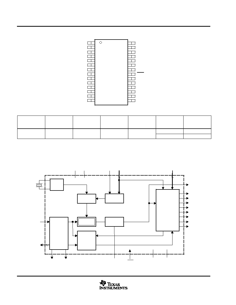
1
2
3
4
5
6
7
8
9
10
11
12
13
14
28
27
26
25
24
23
22
21
20
19
18
17
16
15
ADFLG
BRATE0
BRATE1
SCKO
V
DD
DGND
XTO
XTI
CKTRNS
LRCKO
BCKO
DOUT
SCF0
SCF1
TEST
UNLOCK
FMT1
FMT0
V
CC
AGND
FILT
RST
DIN
BRSEL
BFRAME
EMFLG
URBIT
CSBIT
DIR1701
(TOP VIEW)
PACKAGE/ORDERING INFORMATION
PRODUCT
PACKAGE
PACKAGE
DRAWING
NUMBER
OPERATION
TEMPERATURE
RANGE
PACKAGE
MARKING
ORDERING
NUMBER
}
TRANSPORT
MEDIA
°
°
DIR1701E
Rails
DIR1701E
SSOP28
324
25
°
C to +85
°
C
DIR1701E
DIR1701E/2K
Tape and Reel
TI equivalent no. 4040065.
Models with a slash (/) are available only in tape and reel in the quantities indicated (e.g., /2K indicates 2000 devices per reel). Ordering 2000
pieces of DIR1701E/2K will get a single 2000-piece tape and reel.
block diagram
OSC
OSC
Selector
PLL1
PLL2
SpAct
S/PDIF
DECODER
FIFO
wrclk
rdclk
SCKO
BRSEL
DIN
UNLOCK CKTRNS
BCKO
LRCKO
DOUT
URBIT
CSBIT
ADFLG
EMFLG
100 MHz
SCF
BRATE
FMT
RST
VDD VCC
DGND
AGND
XTI
XTO
2
Audio Clock
and Data
Generator
BFRAME
FILT
DIR1701
SLAS331 APRIL 2001
3
www.ti.com
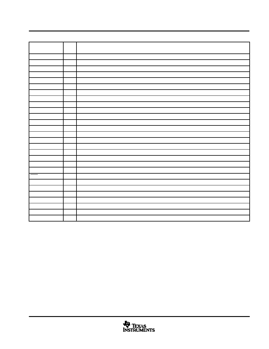
Terminal Functions
TERMINAL
NAME
PIN
I/O
DESCRIPTIONS
ADFLG
1
O
Audio data or digital data flag
BRATE0
2
O
fs rate flag 0 (32k, 44.1k, 48k, and 88k / 96k)
BRATE1
3
O
fs rate flag 1 (32k, 44.1k, 48k, and 88k / 96k)
SCKO
4
O
System clock output
VDD
5
Digital power supply, +3.3 V
DGND
6
Digital ground
XTO
7
O
Crystal oscillator output
XTI
8
I
Crystal oscillator input, external clock input
CKTRNS
9
O
Clock transition status output
LRCKO
10
O
Audio latch enable (LRCK, fs) output
BCKO
11
O
Audio bit clock output
DOUT
12
O
Audio serial data output
SCF0
13
I
System clock frequency select (128/256/384/512 fs) (see Note 1)
SCF1
14
I
System clock frequency select (128/256/384/512 fs) (see Note 1)
CSBIT
15
O
Channel status bit output (see Note 2)
URBIT
16
O
User bit output (see Note 2)
EMFLG
17
O
Emphasis flag
BFRAME
18
O
Block start clock (B-frame)
BRSEL
19
I
Default bit rate select (32 / 44.1 / 48 / 88.2 / 96k) (see Note 1)
DIN
20
I
S/PDIF data digital input (see Note 4)
RST
21
I
Reset input, active LOW (see Note 3)
FILT
22
External filter
AGND
23
Analog ground
VCC
24
Analog power supply, +3.3V
FMT0
25
I
Audio data format select (see Note 1)
FMT1
26
I
Audio data format select (see Note 1)
UNLOCK
27
O
PLL unlock or parity error flag
TEST
28
I
Should be connected to DGND (see Note 1)
NOTES:
1. Schmitt trigger input with internal pulldown (TYP 51 k
), 5 V tolerant.
2. Serial outputs are utilized for both consumer and professional application.
3. Schmitt trigger input with internal pullup (TYP 51 k
), 5 V tolerant.
4. CMOS level input with internal pulldown (TYP 51 k
), 5 V tolerant.

DIR1701
SLAS331 APRIL 2001
4
www.ti.com
absolute maximum ratings
Supply voltage, V
CC
, V
DD
4.0 V
. . . . . . . . . . . . . . . . . . . . . . . . . . . . . . . . . . . . . . . . . . . . . . . . . . . . . . . . . . . . . . . . .
Supply voltage differences, V
CC
, V
DD
±
0.1 V
. . . . . . . . . . . . . . . . . . . . . . . . . . . . . . . . . . . . . . . . . . . . . . . . . . . . . . .
Ground voltage differences, AGND, DGND
±
0.1 V
. . . . . . . . . . . . . . . . . . . . . . . . . . . . . . . . . . . . . . . . . . . . . . . . . .
Digital input voltage:
Digital input pins except XTI
0.3 V to (6.5 V + 0.3 V)
. . . . . . . . . . . . . . . . . . . . . . . . . .
XTI
0.3 V to (V
DD
+ 0.3 V)
. . . . . . . . . . . . . . . . . . . . . . . . . . . . . . . . . . . . . . . . . . . . . . . . .
Input current (Any pins except supplies)
±
10 mA
. . . . . . . . . . . . . . . . . . . . . . . . . . . . . . . . . . . . . . . . . . . . . . . . . . . .
Ambient temperature under bias
40
°
C to 125
°
C
. . . . . . . . . . . . . . . . . . . . . . . . . . . . . . . . . . . . . . . . . . . . . . . . . . . .
Storage temperature
55
°
C to 150
°
C
. . . . . . . . . . . . . . . . . . . . . . . . . . . . . . . . . . . . . . . . . . . . . . . . . . . . . . . . . . . . .
Junction temperature
150
°
C
. . . . . . . . . . . . . . . . . . . . . . . . . . . . . . . . . . . . . . . . . . . . . . . . . . . . . . . . . . . . . . . . . . . . .
Lead temperature (soldering)
260
°
C, 5 sec
. . . . . . . . . . . . . . . . . . . . . . . . . . . . . . . . . . . . . . . . . . . . . . . . . . . . . . . .
Package temperature (IR reflow, peak)
235
°
C, 10 sec
. . . . . . . . . . . . . . . . . . . . . . . . . . . . . . . . . . . . . . . . . . . . . . .
Stresses beyond those listed under "absolute maximum ratings" may cause permanent damage to the device. These are stress ratings only, and
functional operation of the device at these or any other conditions beyond those indicated under "recommended operating conditions" is not
implied. Exposure to absolute-maximum-rated conditions for extended periods may affect device reliability.
DIR1701
SLAS331 APRIL 2001
5
www.ti.com
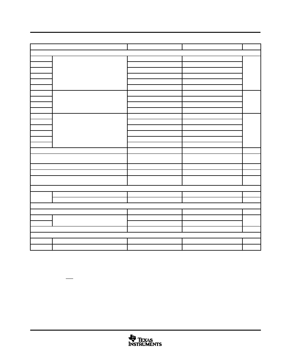
electrical characteristics, all specifications at T
A
= 25
°
C, V
CC
= V
DD
= 3.3 V (unless otherwise noted)
PARAMETER
TEST CONDITIONS
MIN
TYP
MAX
UNIT
DIGITAL INPUT/OUTPUT
VIH (5)
2
5.5
VIL (5)
0.8
VIH2 (6)
70%VDD
VIL2 (6)
Input logic level
30%VDD
VDC
VIH3 (7)
70%VDD
5.5
VIL3 (7)
30%VDD
VOH (8)
IO = 1 mA
VDD0.4
VOL (8)
IO = 2 mA
0.5
VOH (9)
Output logic level
IO = 2 mA
VDD0.4
VDC
VOL (9)
IO = 4 mA
0.5
IIH(10)
VIN = VDD
65
100
IIL(10)
VIN = 0 V
10
10
IIH(11)
VIN = VDD
10
10
µ
IIL(11)
Input leakage current
VIN = 0 V
100
65
µ
A
IIH(6)
VIN = VDD
10
10
IIL(6)
VIN = 0 V
10
10
fs(12)
Input sampling frequency
32
96
kHz
SCKO
System clock frequency
4.096
128/256/
384/512 fs
49.152
MHz
tj
SCKO clock jitter
80
ps RMS
SCKO duty cycle
50%
XTI clock accuracy
500
See
Table 3
500
ppm
S/PDIF INPUT
Duty cycle
VIN = 1.5 V, fs = 96 kHz
15%
85%
Jitter
VIN = 1.5 V
20
ns p-p
POWER SUPPLY REQUIREMENTS
VDD, VCC
Voltage range
3
3.3
3.6
VDC
ICC (VCC)
3.4
4.7
IDD (VDD)
Supply current (see Note 13)
26
36
mA
PD
Power dissipation
100
mW
POWER SUPPLY REQUIREMENTS
Operation temperature
25
85
°
C
JA
Thermal resistance
28-pin SSOP
100
°
C/W
NOTES:
5. TTL compatible, except pins 8, 20: XTI, DIN.
6. Pin 8: XTI (CMOS logic level).
7. Pin 20: DIN (CMOS logic level).
8. Pins 1
3, 9, 17
18, 27: ADFLG, BRATE0, BRATE1, CKTRNS, EMFLG, BFRAME, UNLOCK.
9. Pins 4, 10
12, 15
16: SCKO, LRCKO, BCKO, DOUT, CSBIT, URBIT.
10. Pins 13
14, 19
20, 25
26, 28: SCF0, SCF1, BRSEL, DIN, FMT0, FMT1, CKSEL.
11. Pin 21: RST
12. fs is defined as the incoming audio sampling frequency per channel.
13. No load connected to SCKO, LRCKO, BCKO, DOUT, CSBIT, URBIT. Power supply current varies according to the system clock
frequency.