Äîêóìåíòàöèÿ è îïèñàíèÿ www.docs.chipfind.ru
INA332
INA2332
SBOS216A DECEMBER 2001
www.ti.com
DESCRIPTION
The INA332 and INA2332 are rail-to-rail output, low-power
CMOS instrumentation amplifiers that offer wide range, single-
supply, and bipolar-supply operation. Using a special manu-
facturing flow, the INA332 family provides the lowest cost
available, while still achieving low-noise amplification of dif-
ferential signals with low quiescent current of 415
µ
A (drop-
ping to 0.01
µ
A when shutdown). Returning to normal opera-
tion within microseconds, this INA can be used for battery or
multichannel applications.
Configured internally in a gain of 5V/V, the INA332 offers
flexibility in higher gains by choosing external resistors.
FEATURES
q
DESIGNED FOR LOW COST
q
HIGH GAIN ACCURACY: G = 5, 0.07%, 2ppm/
°
C
q
GAIN SET WITH EXT. RESISTORS FOR > 5V/V
q
HIGH CMRR: 73dB DC, 50dB at 45kHz
q
LOW BIAS CURRENT: 0.5pA
q
BANDWIDTH, SLEW RATE: 2.0MHz, 5V/
µ
s
q
RAIL-TO-RAIL OUTPUT SWING: (V+) 0.02V
q
WIDE TEMPERATURE RANGE: 55
°
C to +125
°
C
q
LOW QUIESCENT CURRENT: 490
µ
A max/chan
q
SHUT DOWN: 0.01
µ
A
q
MSOP-8 SINGLE AND TSSOP-14 DUAL PACKAGES
Copyright © 2001, Texas Instruments Incorporated
Low-Power, Single-Supply, CMOS
INSTRUMENTATION AMPLIFIERS
Please be aware that an important notice concerning availability, standard warranty, and use in critical applications of
Texas Instruments semiconductor products and disclaimers thereto appears at the end of this data sheet.
APPLICATIONS
q
INDUSTRIAL SENSOR AMPLIFIERS:
Bridge, RTD, Thermocouple, Position
q
PHYSIOLOGICAL AMPLIFIERS: ECG, EEG, EMG
q
A/D CONVERTER SIGNAL CONDITIONING
q
DIFFERENTIAL LINE RECEIVERS WITH GAIN
q
FIELD UTILITY METERS
q
PCMCIA CARDS
q
AUDIO AMPLIFIERS
q
COMMUNICATION SYSTEMS
q
TEST EQUIPMENT
q
AUTOMOTIVE INSTRUMENTATION
The INA332 rejects line noise and its harmonics because
common-mode error remains low even at higher frequencies.
High bandwidth and slew rate make the INA332 ideal for
directly driving sampling Analog-to-Digital (A/D) converters
as well as general-purpose applications.
With high precision, low cost, and small packages, the
INA332 outperforms discrete designs.
Additionally, because they are specified for wide temperature
range of 55
°
C to +125
°
C and operating range of 65
°
C to
+150
°
C, the INA331 family can be used in demanding
industrial and automotive environments.
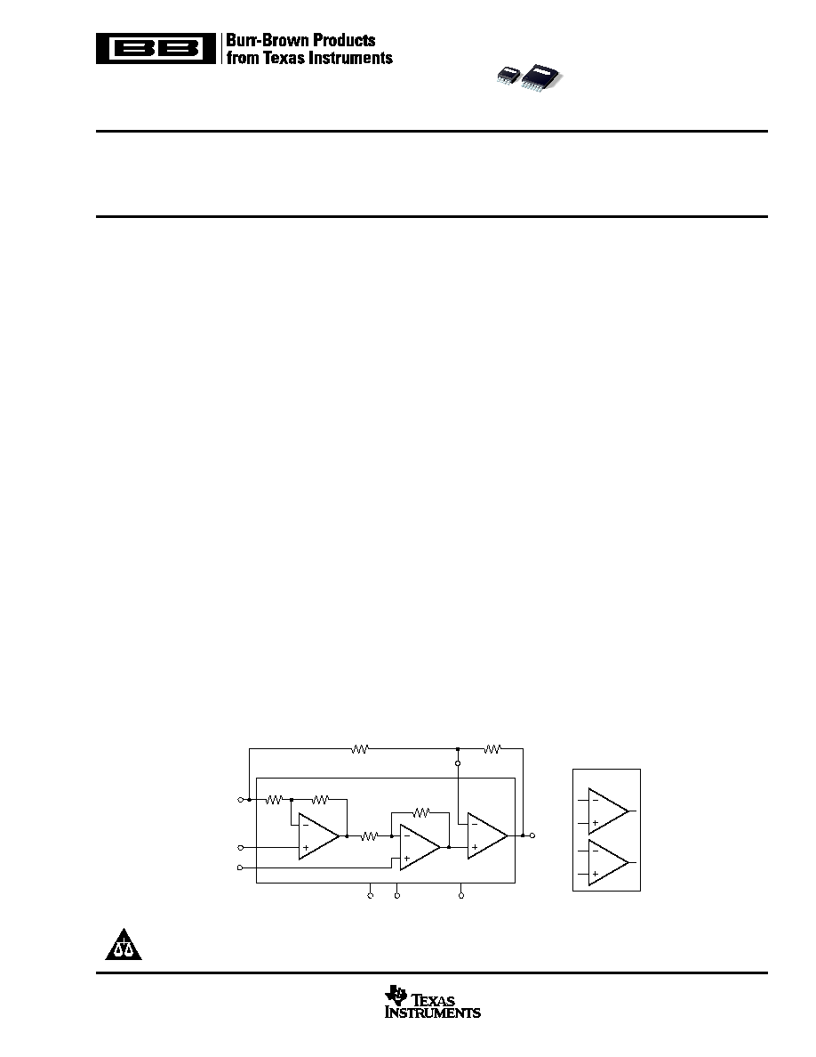
A2
A1
A3
40k
V
REF
V
IN
V
IN
+
10k
10k
Shutdown
V+
V
OUT
G = 5 + (5R
2
/R
1
)
V
R
2
R
1
R
G
40k
Ch A
INA2332
INA332
Ch B
®
INA2
332
INA3
32
PRODUCTION DATA information is current as of publication date.
Products conform to specifications per the terms of Texas Instruments
standard warranty. Production processing does not necessarily include
testing of all parameters.
INA332, INA2332
2
SBOS216A
www.ti.com
Supply Voltage, V+ to V .................................................................... 7.5V
Signal Input Terminals, Voltage
(2)
..................... (V) 0.5V to (V+) + 0.5V
Current
(2)
..................................................... 10mA
Output Short-Circuit
(3)
.............................................................. Continuous
Operating Temperature .................................................. 55
°
C to +125
°
C
Storage Temperature ...................................................... 65
°
C to +150
°
C
Junction Temperature ...................................................................... 150
°
C
Lead Temperature (soldering, 10s) ................................................. 300
°
C
NOTES: (1) Stresses above these ratings may cause permanent damage.
Exposure to absolute maximum conditions for extended periods may degrade
device reliability. (2) Input terminals are diode-clamped to the power-supply rails.
Input signals that can swing more than 0.5V beyond the supply rails should be
current limited to 10mA or less. (3) Short-circuit to ground, one amplifier per
package.
ABSOLUTE MAXIMUM RATINGS
(1)
ELECTROSTATIC
DISCHARGE SENSITIVITY
This integrated circuit can be damaged by ESD. Texas Instru-
ments recommends that all integrated circuits be handled with
appropriate precautions. Failure to observe proper handling
and installation procedures can cause damage.
ESD damage can range from subtle performance degradation
to complete device failure. Precision integrated circuits may be
more susceptible to damage because very small parametric
changes could cause the device not to meet its published
specifications.
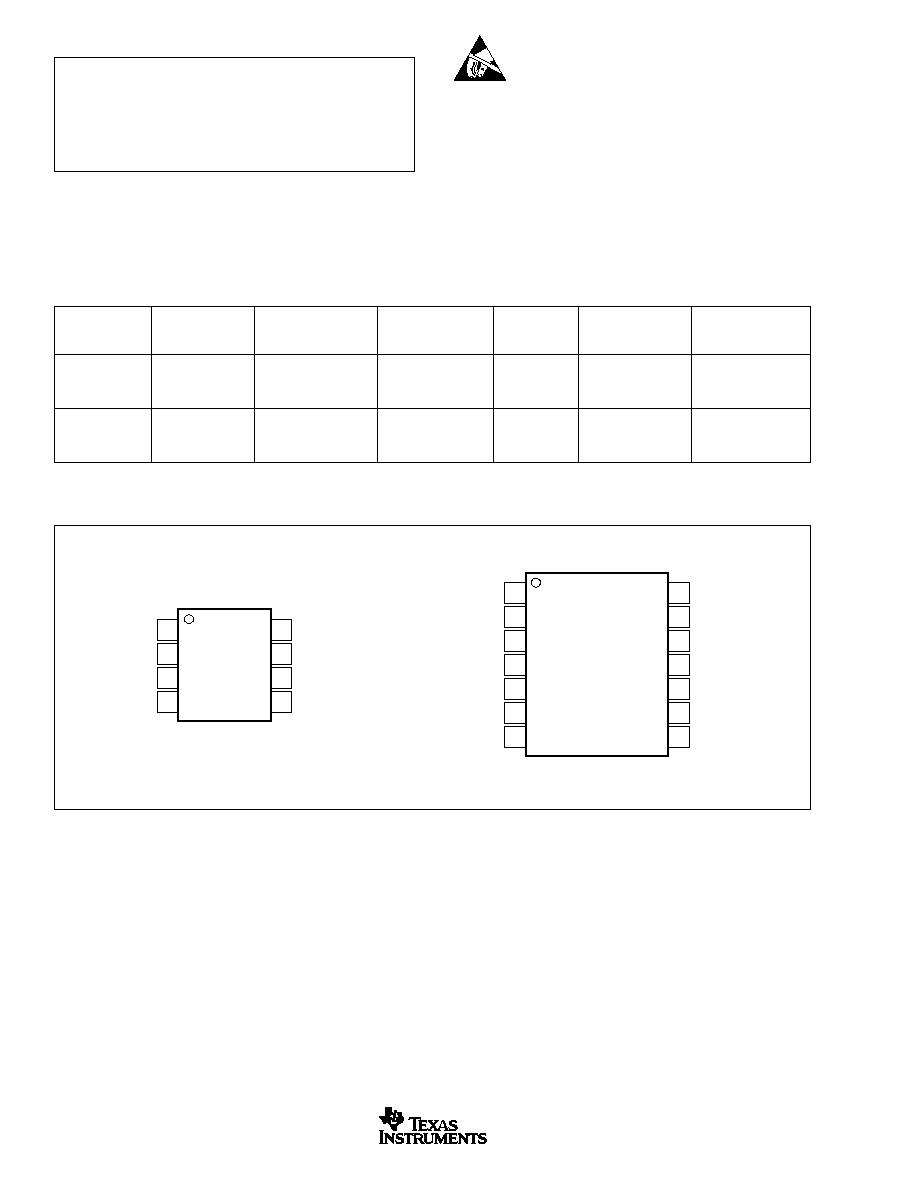
PIN CONFIGURATION
Top View
RG
V
IN
V
IN
+
V
Shutdown
V+
V
OUT
REF
INA332
MSOP-8 (DGK)
1
2
3
4
8
7
6
5
1
2
3
4
5
6
7
14
13
12
11
10
9
8
Shutdown A
V
OUT
A
REFA
V+
REFB
V
OUT
B
Shutdown B
RGA
V
IN
A
V
IN
+A
V
V
IN
+B
V
IN
B
RGB
INA2332
Dual, TSSOP-14 (PW)
SPECIFIED
PACKAGE
TEMPERATURE
PACKAGE
ORDERING
TRANSPORT
PRODUCT
PACKAGE-LEAD
DESIGNATOR
(1)
RANGE
MARKING
NUMBER
MEDIA, QUANTITY
Single
INA332IDGK
MSOP-8
DGK
55
°
C to +125
°
C
B32
INA332IDGKT
Tape and Reel, 250
"
"
"
"
"
INA332IDGKR
Tape and Reel, 2500
Dual
INA2332AIPW
TSSOP-14
PW
55
°
C to +125
°
C
2332A
INA2332AIPWT
Tape and Reel, 250
"
"
"
"
"
INA2332AIPWR
Tape and Reel, 2500
PACKAGE/ORDERING INFORMATION
NOTE: (1) For the most current specifications and package information, refer to our web site at www.ti.com.
INA332, INA2332
3
SBOS216A
www.ti.com
ELECTRICAL CHARACTERISTICS: V
S
= +2.7V TO +5.5V
BOLDFACE limits apply over the specified temperature range, T
A
= 55
°
C TO 125
°
C
At T
A
= +25
°
C, R
L
= 10k
, G = 25, and V
CM
= V
S
/2, unless otherwise noted.
INA332AIDGK
INA2332AIPW
PARAMETER
CONDITION
MIN
TYP
MAX
UNITS
INPUT
Input Offset Voltage, RTI
V
S
= +5V
±
2
±
8
mV
Over Temperature
V
OS
±
9
mV
Temperature Coefficient
dV
OS
/dT
±
5
µ
V/
°
C
vs Power Supply
PSRR
V
S
= +2.7V to +5.5V
±
50
±
250
µ
V/V
Over Temperature
±
260
µ
V/V
Long-Term Stability
±
0.4
µ
V/month
Input Impedance
10
13
|| 3
|| pF
Input Common-Mode Range
V
S
= 2.7V
0.35
1.5
V
V
S
= 5V
0.55
3.8
V
Common-Mode Rejection
CMRR
V
S
= 5V, V
CM
= 0.55V to 3.8V
60
73
dB
Over Temperature
V
S
= 5V, V
CM
= 0.55V to 3.8V
60
dB
V
S
= 2.7V, V
CM
= 0.35V to 1.5V
73
dB
Crosstalk, Dual
114
dB
INPUT BIAS CURRENT
V
CM
= V
S
/2
Bias Current
I
B
±
0.5
±
10
pA
Offset Current
I
OS
±
0.5
±
10
pA
NOISE, RTI
R
S
= 0
Voltage Noise: f = 10Hz
e
N
280
nV/
Hz
f = 100Hz
96
nV/
Hz
f = 1kHz
46
nV/
Hz
f = 0.1Hz to 10Hz
7
µ
Vp-p
Current Noise: f = 1kHz
i
N
0.5
fA/
Hz
GAIN
(1)
Gain Equation, Externally Set
G > 5
G = 5 + 5(R
2
/R
1
)
Range of Gain
5
1000
V/V
Gain Error
±
0.07
±
0.4
%
vs Temperature
G = 5
±
2
±
10
ppm/
°
C
Nonlinearity
G = 25, V
S
= 5V, V
O
= 0.05 to 4.95
±
0.001
±
0.010
% of FS
Over Temperature
±
0.002
±
0.015
% of FS
OUTPUT
Output Voltage Swing from Rail
(2)
G
10
50
25
mV
Over Temperature
50
mV
Capacitance Load Drive
See Typical Characteristics
(3)
pF
Short-Circuit Current
I
SC
+48/32
mA
FREQUENCY RESPONSE
Bandwidth, 3dB
BW
G = 25
2.0
MHz
Slew Rate
SR
V
S
= 5V, G = 25
5
V/
µ
s
Settling Time, 0.1%
t
S
G = 25, C
L
= 100pF, V
O
= 2V step
1.7
µ
s
0.01%
2.5
µ
s
Overload Recovery
50% Input Overload G = 25
2
µ
s
POWER SUPPLY
Specified Voltage Range
+2.7
+5.5
V
Operating Voltage Range
+2.5 to +5.5
V
Quiescent Current per Channel
I
Q
V
SD
> 2.5
(4)
415
490
µ
A
Over Temperature
600
µ
A
Shutdown Quiescent Current/Chan
I
SD
V
SD
< 0.8
(4)
0.01
1
µ
A
TEMPERATURE RANGE
Specified Range
55
+125
°
C
Operating/Storage Range
65
+150
°
C
Thermal Resistance
JA
MSOP-8, TSSOP-14 Surface Mount
150
°
C/W
NOTES: (1) Does not include errors from external gain setting resistors (2) Output voltage swings are measured between the output and power-supply rails. Output
swings to rail only if G
10. Output does not swing to positive rail if gain is less than 10. (3) See typical characteristic "Percent Overshoot vs Load Capacitance."
(4) See typical characteristic "Shutdown Voltage vs Supply Voltage."
INA332, INA2332
4
SBOS216A
www.ti.com
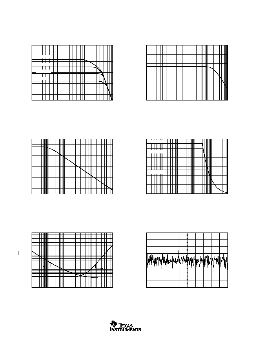
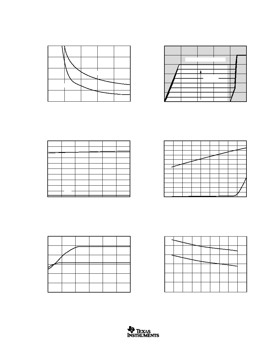
TYPICAL CHARACTERISTICS
At T
A
= +25
°
C, V
S
= 5V, V
CM
= V
S
/2, R
L
= 10k
, and C
L
= 100pF, unless otherwise noted.
GAIN vs FREQUENCY
10
Gain (dB)
Frequency (Hz)
100
1k
10k
100k
1M
10M
80
70
60
50
40
30
20
10
0
10
20
Gain = 500
Gain = 100
Gain = 25
Gain = 5
COMMON-MODE REJECTION RATIO
vs FREQUENCY
10
CMRR (dB)
Frequency (Hz)
100
1k
10k
100k
120
100
80
60
40
20
0
POWER-SUPPLY REJECTION RATIO
vs FREQUENCY
1
PSRR (dB)
Frequency (Hz)
10
100
1k
10k
100k
100
90
80
70
60
50
40
30
20
10
0
MAXIMUM OUTPUT VOLTAGE vs FREQUENCY
100
Maximum Output Voltage (Vp-p)
Frequency (Hz)
1k
10k
100k
1M
10M
6
5
4
3
2
1
0
V
S
= 5.5V
V
S
= 5.0V
V
S
= 2.7V
NOISE vs FREQUENCY
1
V
NOISE
(nV/
Hz)
I
NOISE
(fA/
Hz)
Frequency (Hz)
10
100
1k
10k
100k
10k
1k
100
10
100
10
1
0.1
0.1Hz TO 10Hz VOLTAGE NOISE
1s/div
2
µ
V/div
INA332, INA2332
5
SBOS216A
www.ti.com
TYPICAL CHARACTERISTICS
(Cont.)
At T
A
= +25
°
C, V
S
= 5V, V
CM
= V
S
/2, R
L
= 10k
, and C
L
= 100pF, unless otherwise noted.
OUTPUT SWING vs LOAD RESISTANCE
Swing to Rail (mV)
R
LOAD
(
)
0
10k
20k
30k
40k
50k
25
20
15
10
5
0
To Positive Rail
To Negative Rail
COMMON-MODE INPUT RANGE
vs REFERENCE VOLTAGE
0
Output
--
Referred to Ground (V)
Input Common-Mode Voltage (V)
1
2
3
4
5
6
5
4
3
2
1
0
Outside of Normal Operation
REF
Increasing
QUIESCENT CURRENT AND SHUTDOWN CURRENT
vs POWER SUPPLY
I
Q
(
µ
A), I
SD
(nA)
Supply Voltage (V)
2.5
3
3.5
4
4.5
5
5.5
500
450
400
350
300
250
200
150
100
50
0
I
Q
I
SD
QUIESCENT CURRENT AND SHUTDOWN CURRENT
vs TEMPERATURE
I
Q
(
µ
A)
Temperature (
°
C)
75
50
25
0
25
50
75
100
125
150
600
550
500
450
400
350
300
250
200
150
100
50
0
I
Q
I
SD
SHORT-CIRCUIT CURRENT vs POWER SUPPLY
I
SC
(mA)
Supply Voltage (V)
2.5
3
3.5
4
4.5
5
5.5
60
50
40
30
20
10
0
I
SC+
I
SC
SHORT-CIRCUIT CURRENT vs TEMPERATURE
I
SC
(mA)
Temperature (
°
C)
75
25
50
25
0
50
75
100
125
150
60
50
40
30
20
10
0
I
SC+
I
SC
INA332, INA2332
6
SBOS216A
www.ti.com
TYPICAL CHARACTERISTICS
(Cont.)
At T
A
= +25
°
C, V
S
= 5V, V
CM
= V
S
/2, R
L
= 10k
, and C
L
= 100pF, unless otherwise noted.
SMALL-SIGNAL STEP RESPONSE (G = 5)
4
µ
s/div
100mV/div
SMALL-SIGNAL STEP RESPONSE (G = 100)
4
µ
s/div
50mV/div
SMALL-SIGNAL STEP RESPONSE
(G = 5, C
L
= 1000pF)
4
µ
s/div
100mV/div
SMALL-SIGNAL STEP RESPONSE
(G = 100, C
L
= 1000pF)
10
µ
s/div
50mV/div
SMALL-SIGNAL STEP RESPONSE
(G = 100, C
L
= 4700pF)
10
µ
s/div
50mV/div
LARGE-SIGNAL STEP RESPONSE (G = 25)
10
µ
s/div
1V/div
INA332, INA2332
7
SBOS216A
www.ti.com
TYPICAL CHARACTERISTICS
(Cont.)
At T
A
= +25
°
C, V
S
= 5V, V
CM
= V
S
/2, R
L
= 10k
, and C
L
= 100pF, unless otherwise noted.
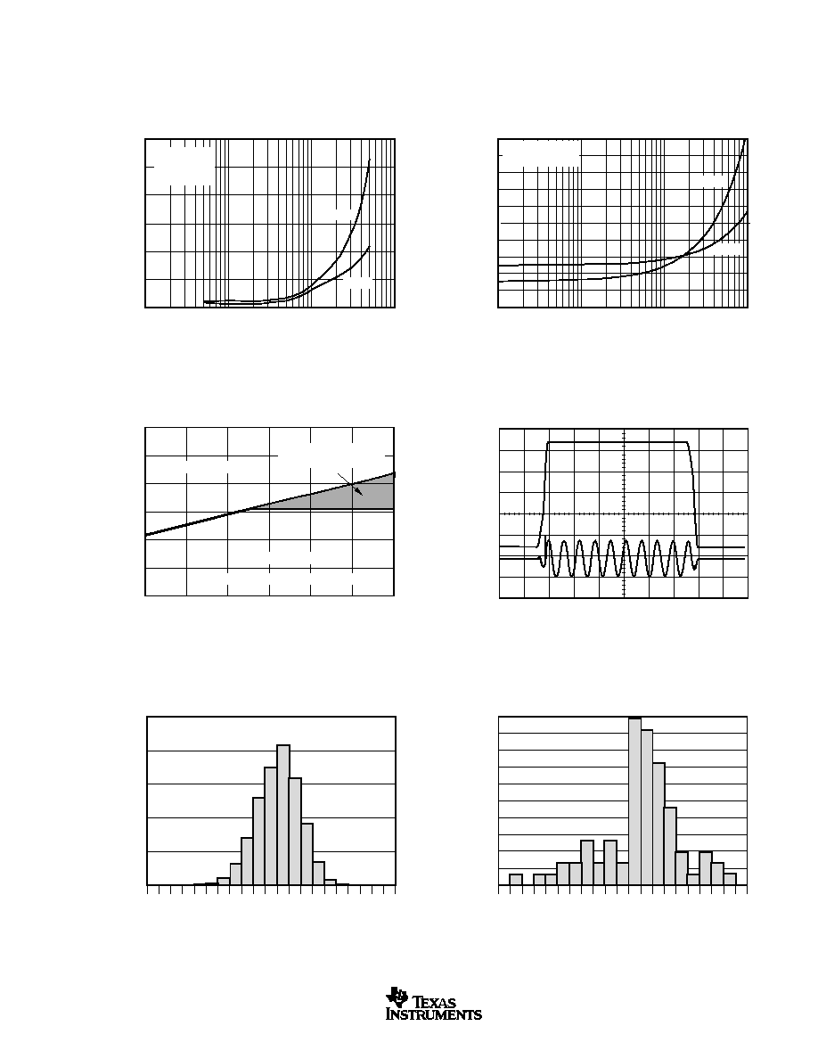
SETTLING TIME vs GAIN
1
10
100
1k
Gain (V/V)
Settling Time (
µ
s)
60
50
40
30
20
10
0
Output 2Vp-p
Differential
Input Drive
0.01%
0.1%
PERCENT OVERSHOOT vs LOAD CAPACITANCE
10
100
1k
10k
Load Capacitance (pF)
Overshoot (%)
100
90
80
70
60
50
40
30
20
10
0
Output 100mVp-p
Differential Drive
G = 5
G = 25
SHUTDOWN VOLTAGE vs SUPPLY VOLTAGE
2.5
Shutdown (V)
Supply Voltage (V)
3
3.5
4
4.5
5
5.5
3
2.5
2
1.5
1
0.5
0
Normal Operation Mode
Part Draws Below 1
µ
A Quiescent Current
Operation in this Region
is not Recommended
Shutdown Mode
SHUTDOWN TRANSIENT BEHAVIOR
50
µ
s/div
1V/div
V
SD
V
OUT
25
20
15
10
5
0
10
9
8
7
6
5
4
3
2
1
0
1
2
3
4
5
6
7
8
9
10
Offset Voltage (mV)
Percentage of Amplifiers (%)
OFFSET VOLTAGE PRODUCTION DISTRIBUTION
20
18
16
14
12
10
8
6
4
2
0
14
13
11
10
8
7
6
4
3
1
0
1
3
4
6
7
8
10
11
13
14
Offset Voltage (
µ
V/
°
C)
Percentage of Amplifiers (%)
OFFSET VOLTAGE DRIFT
PRODUCTION DISTRIBUTION
INA332, INA2332
8
SBOS216A
www.ti.com
TYPICAL CHARACTERISTICS
(Cont.)
At T
A
= +25
°
C, V
S
= 5V, V
CM
= V
S
/2, R
L
= 10k
, and C
L
= 100pF, unless otherwise noted.
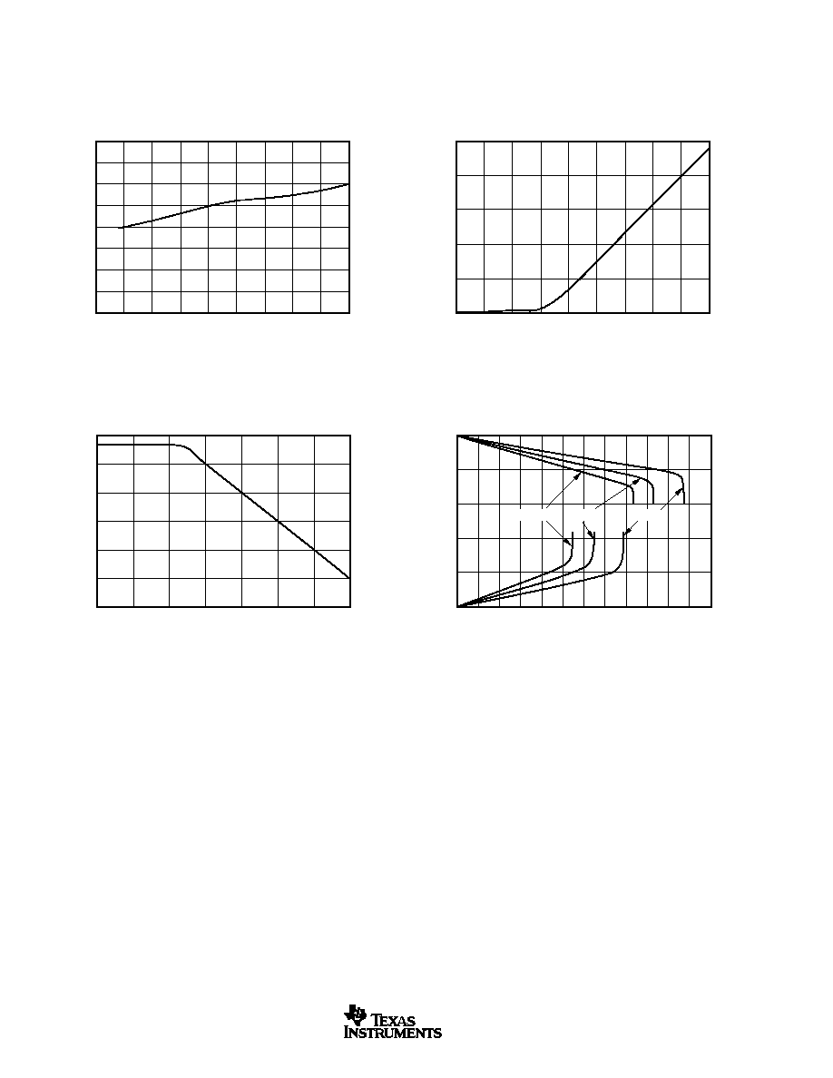
SLEW RATE vs TEMPERATURE
Slew Rate (V/
µ
s)
Temperature (
°
C)
75
25
50
25
0
50
75
100
125
150
8
7
6
5
4
3
2
1
0
OUTPUT VOLTAGE SWING vs OUTPUT CURRENT
Output Voltage (V)
Output Current (mA)
0
5
10
15
25
35
45
55
20
30
40
50
60
5
4
3
2
1
0
125
°
C
25
°
C
55
°
C
INPUT BIAS CURRENT vs TEMPERATURE
Input Bias Current (pA)
Temperature (
°
C)
75
25
50
25
0
50
75
100
125
150
10000
1000
100
10
1
0.1
CHANNEL SEPARATION vs FREQUENCY
Separation (dB)
Frequency (Hz)
1
10k
10
100
1k
100k
1M
10M
120
100
80
60
40
20
0
INA332, INA2332
9
SBOS216A
www.ti.com
APPLICATIONS INFORMATION
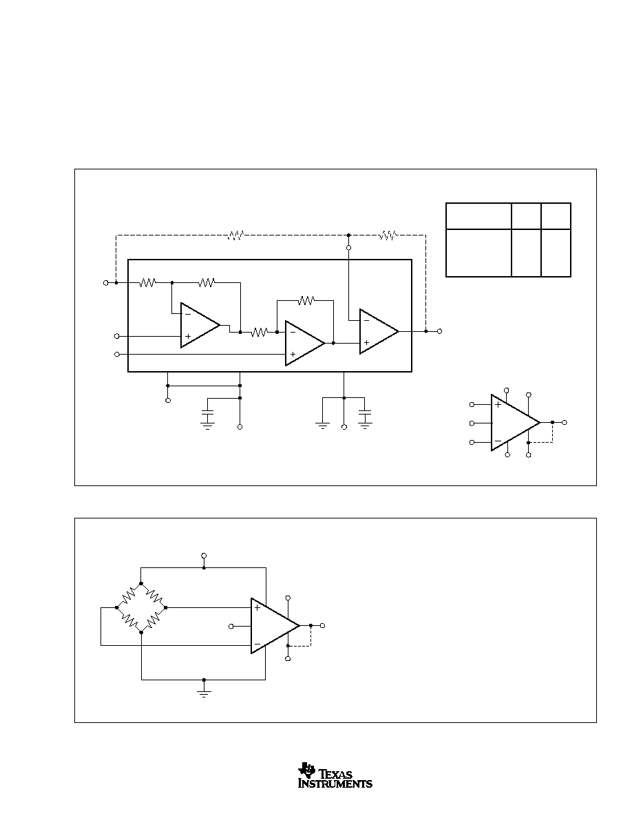
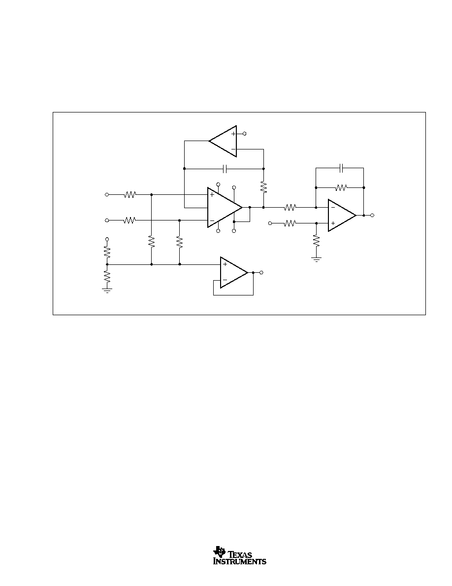
The INA332 is a modified version of the classic "two op amp"
instrumentation amplifier, with an additional gain amplifier.
Figure 1 shows the basic connections for the operation of the
INA332 and INA2332. The power supply should be capaci-
tively decoupled with 0.1
µ
F capacitors as close to the INA332
as possible for noisy or high-impedance applications.
The output is referred to the reference terminal, which must
be at least 1.2V below the positive supply rail.
OPERATING VOLTAGE
The INA332 family is fully specified over a supply range of
+2.7V to +5.5V, with key parameters tested over the tempera-
ture range of 55
°
C to +125
°
C. Parameters that vary signifi-
cantly with operating conditions, such as load conditions or
temperature, are shown in the Typical Characteristics.
The INA332 may be operated on a single supply. Figure 2
shows a bridge amplifier circuit operated from a single +5V
supply. The bridge provides a small differential voltage riding
on an input common-mode voltage.
FIGURE 2. Single-Supply Bridge Amplifier.
FIGURE 1. Basic Connections.
40k
10k
10k
40k
3
2
5
1
7
8
4
Also drawn in simplified form:
6
REF
0.1
µ
F
0.1
µ
F
RG
V
IN
V
IN
+
V
V+
A1
A3
A2
V
O
= ((V
IN
+) (V
IN
)) · G
Short V
OUT
to RG
for G = 5
5
10
50
100
SHORT
100k
90k
190k
OPEN
100k
10k
10k
R
2
R
1
Shutdown
(For Single
Supply)
DESIRED GAIN
(V/V)
R
1
R
2
G = 5 + 5 (R
2
/ R
1
)
INA332
5
3
2
V
OUT
8
7
6
4
1
V+
Shutdown
RG
V
IN
V
V
IN
+
REF
Bridge
Sensor
+5V
NOTE: (1) REF should be adjusted for the desired output level,
keeping in mind that the value of REF affects the common-mode
input range. See Typical Characteristics.
INA332
5
3
2
V
OUT
8
7
6
4
1
V+
Shutdown
RG
V
IN
V
V
IN
+
REF
(1)
INA332, INA2332
10
SBOS216A
www.ti.com
SETTING THE GAIN
The ratio of R
2
to R
1
, or the impedance between pins 1, 5,
and 6, determines the gain of the INA332. With an internally
set gain of 5, the INA332 can be programmed for gains
greater than 5 according to the following equation:
G = 5 + 5 (R
2
/R
1
)
The INA332 is designed to provide accurate gain, with gain
error less than 0.4%. Setting gain with matching TC resistors
will minimize gain drift. Errors from external resistors will add
directly to the error, and may become dominant error sources.
COMMON-MODE INPUT RANGE
The upper limit of the common-mode input range is set by the
common-mode input range of the second amplifier, A2, to
1.2V below positive supply. Under most conditions, the
amplifier operates beyond this point with reduced perfor-
mance. The lower limit of the input range is bounded by the
output swing of amplifier A1, and is a function of the refer-
ence voltage according to the following equation:
V
OA1
= 5/4 V
CM
1/4 V
REF
(See typical characteristic "Common-Mode Input Range vs
Reference Voltage").
REFERENCE
The reference terminal defines the zero output voltage level.
In setting the reference voltage, the common mode input of
A3 should be considered according to the following equation:
V
OA2
= V
REF
+ 5 (V
IN
+ V
IN
)
For ensured operation, V
OA2
should be less than V
DD
1.2V.
The reference pin requires a low-impedance connection. As
little as 160
in series with the reference pin will degrade the
CMRR to 50dB. The reference pin may be used to compen-
sate for the offset voltage (see Offset Trimming section). The
reference voltage level also influences the common-mode
input range (see Common-Mode Input Range section).
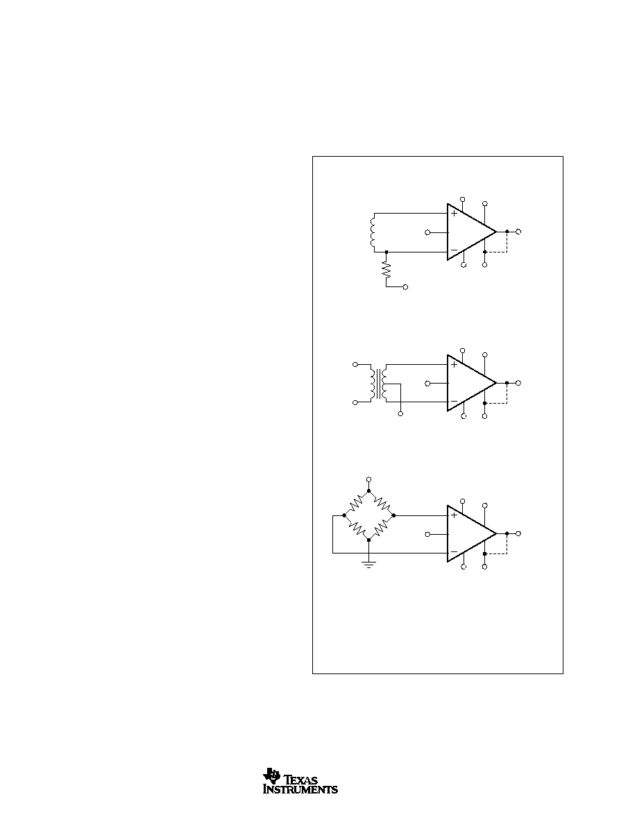
INPUT BIAS CURRENT RETURN
With a high input impedance of 10
13
, the INA332 is ideal for
use with high-impedance sources. The input bias current of
less than 10pA makes the INA332 nearly independent of
input impedance and ideal for low-power applications.
For proper operation, a path must be provided for input bias
currents for both inputs. Without input bias current paths, the
inputs will "float" to a potential that exceeds common-mode
range and the input amplifier will saturate. Figure 3 shows
FIGURE 3. Providing an Input Common-Mode Path.
how bias current path can be provided in the cases of
microphone applications, thermistor applications, ground re-
turns, and dc-coupled resistive bridge applications.
When differential source impedance is low, the bias current
return path can be connected to one input. With higher
source impedance, two equal resistors will provide a bal-
anced input. The advantages are lower input offset voltage
due to bias current flowing through the source impedance
and better high-frequency gain.
47k
Microphone,
Hydrophone,
etc.
Center-tap
provides bias
current return
Bridge resistance
provides bias
current return
Transformer
Bridge
Amplifier
Bridge
Sensor
V
B
(1)
V
B
(1)
V
EX
NOTE: (1) V
B
is bias voltage within
common-mode range, dependent
on REF.
INA332
5
3
2
8
7
6
4
1
V+
Shutdown
V
IN
V
V
IN
+
REF
INA332
5
3
2
8
7
6
4
1
V+
Shutdown
V
IN
V
V
IN
+
REF
INA332
5
3
2
8
7
6
4
1
V+
Shutdown
V
IN
V
V
IN
+
REF
V
OUT
RG
V
OUT
RG
V
OUT
RG
INA332, INA2332
11
SBOS216A
www.ti.com
SHUTDOWN MODE
The shutdown pin of the INA332 is nominally connected to V+.
When the pin is pulled below 0.8V on a 5V supply, the INA332
goes into sleep mode within nanoseconds. For actual shut-
down threshold, see typical characteristic "Shutdown Voltage
vs Supply Voltage". Drawing less than 2
µ
A of current, and
returning from sleep mode in microseconds, the shutdown
feature is useful for portable applications. Once in `sleep-
mode' the amplifier has high output impedance, making the
INA332 suitable for multiplexing.
RAIL-TO-RAIL OUTPUT
A class AB output stage with common-source transistors is
used to achieve rail-to-rail output for gains of 10 or greater.
For resistive loads greater than 10k
, the output voltage can
swing to within 25mV of the supply rail while maintaining low
gain error. For heavier loads and over temperature, see the
typical characteristic "Output Voltage Swing vs Output Cur-
rent." The INA332's low output impedance at high frequencies
makes it suitable for directly driving Capacitive-Input A/D
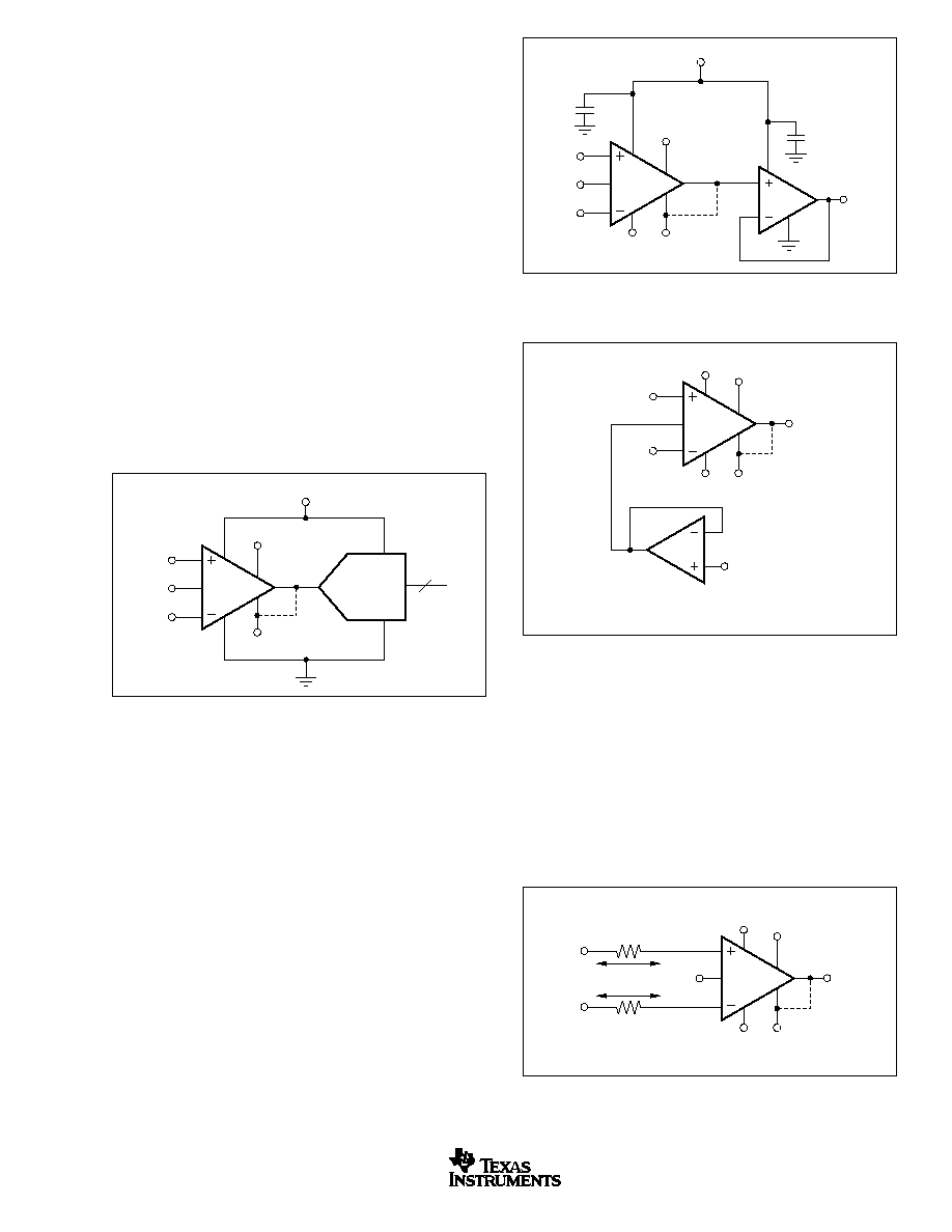
converters, as shown in Figure 4.
FIGURE 4. INA332 Directly Drives Capacitive-Input, High-
Speed A/D Converter.
OUTPUT BUFFERING
The INA332 is optimized for a load impedance of 10k
or
greater. For higher output current the INA332 can be buff-
ered using the OPA340, as shown in Figure 5. The OPA340
can swing within 50mV of the supply rail, driving a 600
load.
The OPA340 is available in the tiny MSOP-8 package.
OFFSET TRIMMING
The INA332 is laser trimmed for low offset voltage. In the
event that external offset adjustment is required, the offset
can be adjusted by applying a correction voltage to the
reference terminal. Figure 6 shows an optional circuit for
trimming offset voltage. The voltage applied to the REF
terminal is added to the output signal. The gain from REF to
V
OUT
is +1. An op amp buffer is used to provide low
impedance at the REF terminal to preserve good common-
mode rejection.
FIGURE 7. Sample Output Buffering Circuit.
INPUT PROTECTION
Device inputs are protected by ESD diodes that will conduct
if the input voltages exceed the power supplies by more than
500mV. Momentary voltages greater than 500mV beyond
the power supply can be tolerated if the current through the
input pins is limited to 10mA. This is easily accomplished with
input resistor R
LIM
, as shown in Figure 7. Many input signals
are inherently current-limited to less than 10mA, therefore, a
limiting resistor is not required.
FIGURE 5. Output Buffering Circuit. Able to drive loads as
low as 600
.
FIGURE 6. Optional Offset Trimming Voltage.
ADS7818
or
ADS7822
12-Bits
+5V
INA332
5
3
2
V
OUT
8
7
6
4
1
V+
Shutdown
RG
V
IN
V
V
IN
+
REF
f
S
< 100kHz
OPA340
V
OUT
+5V
0.1
µ
F
0.1
µ
F
INA332
5
3
2
V
OUT
8
7
6
4
1
V+
Shutdown
RG
V
IN
V
V
IN
+
REF
OPA336
Adjustable
Voltage
INA332
5
3
2
V
OUT
8
7
6
4
1
V+
Shutdown
RG
V
IN
V
V
IN
+
REF
(1)
NOTE: (1) REF should be adjusted for the desired output level.
The value of REF affects the common-mode input range.
R
LIM
R
LIM
I
OVERLOAD
10mA max
INA332
5
3
2
V
OUT
8
7
6
4
1
V+
Shutdown
RG
V
IN
V
V
IN
+
REF
INA332, INA2332
12
SBOS216A
www.ti.com
OFFSET VOLTAGE ERROR CALCULATION
The offset voltage (V
OS
) of the INA332AIDGK is specified at
a maximum of 500
µ
V with a +5V power supply and the
common-mode voltage at V
S
/2. Additional specifications for
power-supply rejection and common-mode rejection are pro-
vided to allow the user to easily calculate worst-case ex-
pected offset under the conditions of a given application.
Power-Supply Rejection Ratio (PSRR) is specified in
µ
V/V.
For the INA332, worst case PSRR is 200
µ
V/V, which means
for each volt of change in power supply, the offset may shift
up to 200
µ
V. Common-Mode Rejection Ratio (CMRR) is
specified in dB, which can be converted to
µ
V/V using the
following equation:
CMRR (in
µ
V/V) = 10
[(CMRR in dB)/20]
· 10
6
For the INA332, the worst case CMRR over the specified
common-mode range is 60dB (at G = 25) or about 30
µ
V/V
This means that for every volt of change in common-mode,
the offset will shift less than 30
µ
V.
These numbers can be used to calculate excursions from the
specified offset voltage under different application condi-
tions. For example, an application might configure the ampli-
fier with a 3.3V supply with 1V common-mode. This configu-
ration varies from the specified configuration, representing a
1.7V variation in power supply (5V in the offset specification
versus 3.3V in the application) and a 0.65V variation in
common-mode voltage from the specified V
S
/2.
Calculation of the worst-case expected offset would be as
follows:
Adjusted V
OS
= Maximum specified V
OS
+
(power-supply variation) · PSRR +
(common-mode variation) · CMRR
V
OS
= 0.5mV + (1.7V · 200
µ
V) + (0.65V · 30
µ
V)
=
±
0.860mV
However, the typical value will be smaller, as seen in the
Typical Characteristics.
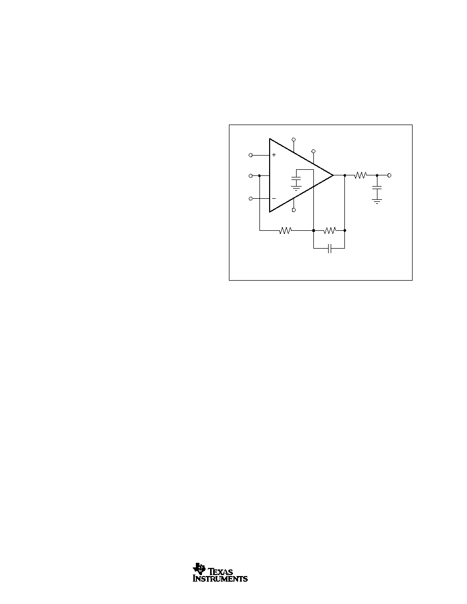
FEEDBACK CAPACITOR IMPROVES RESPONSE
For optimum settling time and stability with high-impedance
feedback networks, it may be necessary to add a feedback
capacitor across the feedback resistor, R
F
, as shown in
Figure 8. This capacitor compensates for the zero created by
the feedback network impedance and the INA332's RG-pin
input capacitance (and any parasitic layout capacitance).
The effect becomes more significant with higher impedance
networks. Also, R
X
and C
L
can be added to reduce high-
frequency noise.
It is suggested that a variable capacitor be used for the
feedback capacitor since input capacitance may vary be-
tween instrumentation amplifiers, and layout capacitance is
difficult to determine. For the circuit shown in Figure 8, the
value of the variable feedback capacitor should be chosen by
the following equation:
R
IN
· C
IN
= R
F
· C
F
Where C
IN
is equal to the INA332's RG-pin input capacitance
(typically 3pF) plus the layout capacitance. The capacitor can
be varied until optimum performance is obtained.
FIGURE 8. Feedback Capacitor Improves Dynamic Perfor-
mance.
INA332
V+
V
OUT
R
IN
R
IN
· C
IN
= R
F
·
C
F
R
F
R
X
C
L
C
IN
Where C
IN
is equal to the INA332's input capacitance
(approximately 3pF) plus any parastic layout capacitance.
5
3
2
8
7
6
4
1
Shutdown
RG
V
IN
V
V
IN
+
REF
C
F
INA332, INA2332
13
SBOS216A
www.ti.com
APPLICATION CIRCUITS
MEDICAL ECG APPLICATIONS
Figure 9 shows the INA332 configured to serve as a low-cost
ECG amplifier, suitable for moderate accuracy heart-rate
applications such as fitness equipment. The input signals are
obtained from the left and right arms of the patient. The
common-mode voltage is set by two 2M
resistors. This
potential through a buffer provides optional right leg drive.
Filtering can be modified to suit application needs by chang-
ing the capacitor value of the output filter.
LOW-POWER, SINGLE-SUPPLY DATA
ACQUISITION SYSTEMS
Refer to Figure 4 to see the INA332 configured to drive an
ADS7818. Functioning at frequencies of up to 500kHz, the
INA332 is ideal for low-power data acquisition.
FIGURE 9. Simplified ECG Circuit for Medical Applications.
OPA336
OPA336
OPA336
Right Arm
Left Arm
1M
REF
1M
1M
10k
10k
2k
2k
1.6nF
0.1
µ
F
100k
100k
+5V
V
R
V
R
V
R
= +2.5V
2M
2M
Right
Leg
INA332
5
3
2
8
7
6
4
1
V+
Shutdown
RG
V
IN
V
V
IN
+
V
OUT PUT
INA332, INA2332
14
SBOS216A
www.ti.com
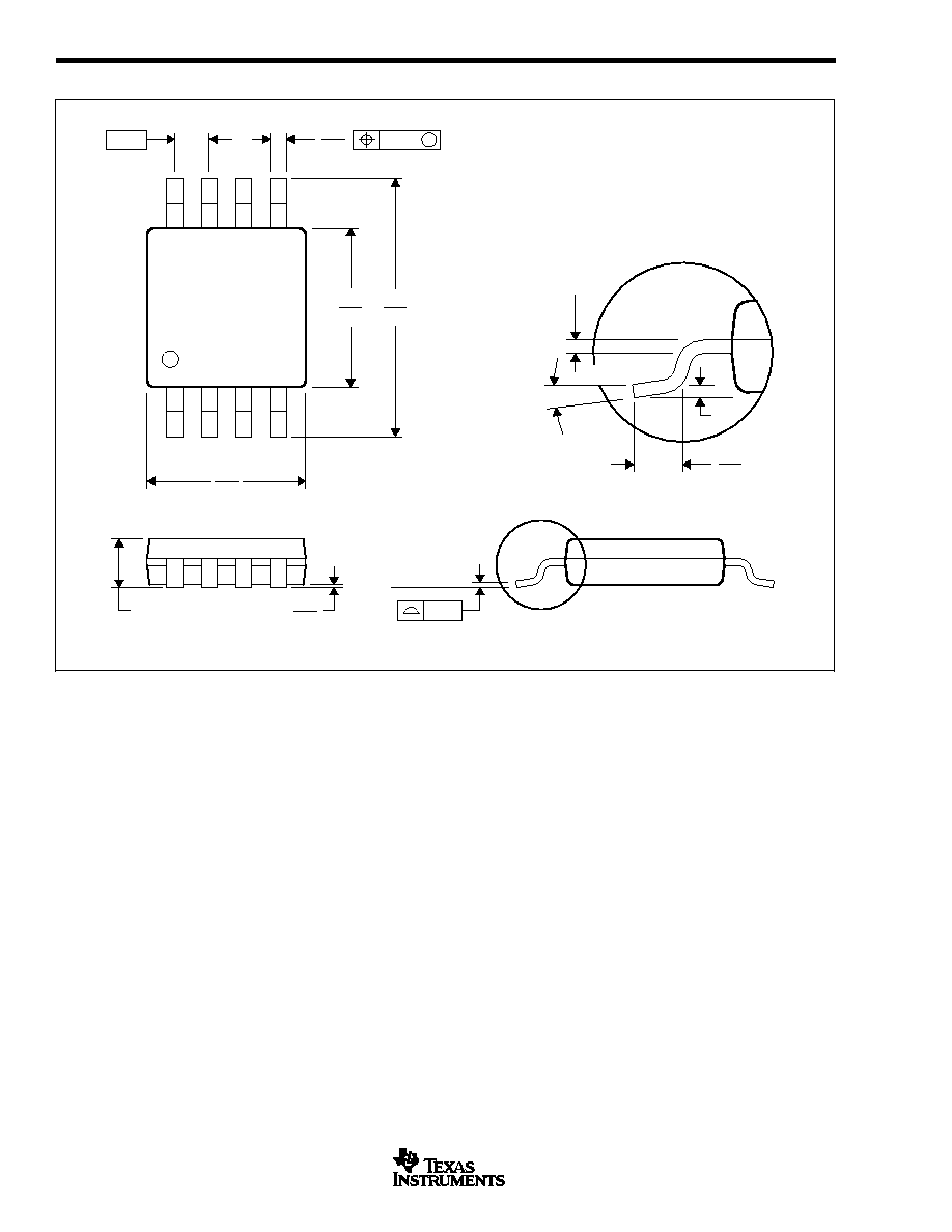
PACKAGE DRAWINGS
MPDS028B JUNE 1997 REVISED SEPTEMBER 2001
DGK (R-PDSO-G8)
PLASTIC SMALL-OUTLINE PACKAGE
0,69
0,41
0,25
0,15 NOM
Gage Plane
4073329/C 08/01
4,98
0,25
5
3,05
4,78
2,95
8
4
3,05
2,95
1
0,38
1,07 MAX
Seating Plane
0,65
M
0,08
0
°
6
°
0,10
0,15
0,05
NOTES: A. All linear dimensions are in millimeters.
B. This drawing is subject to change without notice.
C. Body dimensions do not include mold flash or protrusion.
D. Falls within JEDEC MO-187
INA332, INA2332
15
SBOS216A
www.ti.com
PACKAGE DRAWINGS (Cont.)
MTSS001C JANUARY 1995 REVISED FEBRUARY 1999
PW (R-PDSO-G**)
PLASTIC SMALL-OUTLINE PACKAGE
14 PINS SHOWN
0,65
M
0,10
0,10
0,25
0,50
0,75
0,15 NOM
Gage Plane
28
9,80
9,60
24
7,90
7,70
20
16
6,60
6,40
4040064/F 01/97
0,30
6,60
6,20
8
0,19
4,30
4,50
7
0,15
14
A
1
1,20 MAX
14
5,10
4,90
8
3,10
2,90
A MAX
A MIN
DIM
PINS **
0,05
4,90
5,10
Seating Plane
0
°
8
°
NOTES: A. All linear dimensions are in millimeters.
B. This drawing is subject to change without notice.
C. Body dimensions do not include mold flash or protrusion not to exceed 0,15.
D. Falls within JEDEC MO-153
PACKAGING INFORMATION
Orderable Device
Status
(1)
Package
Type
Package
Drawing
Pins Package
Qty
Eco Plan
(2)
Lead/Ball Finish
MSL Peak Temp
(3)
INA2332AIPWR
ACTIVE
TSSOP
PW
14
2500
TBD
CU NIPDAU
Level-3-240C-168 HR
INA2332AIPWT
ACTIVE
TSSOP
PW
14
250
TBD
CU NIPDAU
Level-3-240C-168 HR
INA332AIDGKR
ACTIVE
MSOP
DGK
8
2500
TBD
CU NIPDAU
Level-1-220C-UNLIM
INA332AIDGKT
ACTIVE
MSOP
DGK
8
250
TBD
CU NIPDAU
Level-1-220C-UNLIM
(1)
The marketing status values are defined as follows:
ACTIVE: Product device recommended for new designs.
LIFEBUY: TI has announced that the device will be discontinued, and a lifetime-buy period is in effect.
NRND: Not recommended for new designs. Device is in production to support existing customers, but TI does not recommend using this part in
a new design.
PREVIEW: Device has been announced but is not in production. Samples may or may not be available.
OBSOLETE: TI has discontinued the production of the device.
(2)
Eco
Plan
-
The
planned
eco-friendly
classification:
Pb-Free
(RoHS)
or
Green
(RoHS
&
no
Sb/Br)
-
please
check
http://www.ti.com/productcontent
for the latest availability information and additional product content details.
TBD: The Pb-Free/Green conversion plan has not been defined.
Pb-Free (RoHS): TI's terms "Lead-Free" or "Pb-Free" mean semiconductor products that are compatible with the current RoHS requirements
for all 6 substances, including the requirement that lead not exceed 0.1% by weight in homogeneous materials. Where designed to be soldered
at high temperatures, TI Pb-Free products are suitable for use in specified lead-free processes.
Green (RoHS & no Sb/Br): TI defines "Green" to mean Pb-Free (RoHS compatible), and free of Bromine (Br) and Antimony (Sb) based flame
retardants (Br or Sb do not exceed 0.1% by weight in homogeneous material)
(3)
MSL, Peak Temp. -- The Moisture Sensitivity Level rating according to the JEDEC industry standard classifications, and peak solder
temperature.
Important Information and Disclaimer:The information provided on this page represents TI's knowledge and belief as of the date that it is
provided. TI bases its knowledge and belief on information provided by third parties, and makes no representation or warranty as to the
accuracy of such information. Efforts are underway to better integrate information from third parties. TI has taken and continues to take
reasonable steps to provide representative and accurate information but may not have conducted destructive testing or chemical analysis on
incoming materials and chemicals. TI and TI suppliers consider certain information to be proprietary, and thus CAS numbers and other limited
information may not be available for release.
In no event shall TI's liability arising out of such information exceed the total purchase price of the TI part(s) at issue in this document sold by TI
to Customer on an annual basis.
PACKAGE OPTION ADDENDUM
www.ti.com
30-Mar-2005
Addendum-Page 1

IMPORTANT NOTICE
Texas Instruments Incorporated and its subsidiaries (TI) reserve the right to make corrections, modifications,
enhancements, improvements, and other changes to its products and services at any time and to discontinue
any product or service without notice. Customers should obtain the latest relevant information before placing
orders and should verify that such information is current and complete. All products are sold subject to TI's terms
and conditions of sale supplied at the time of order acknowledgment.
TI warrants performance of its hardware products to the specifications applicable at the time of sale in
accordance with TI's standard warranty. Testing and other quality control techniques are used to the extent TI
deems necessary to support this warranty. Except where mandated by government requirements, testing of all
parameters of each product is not necessarily performed.
TI assumes no liability for applications assistance or customer product design. Customers are responsible for
their products and applications using TI components. To minimize the risks associated with customer products
and applications, customers should provide adequate design and operating safeguards.
TI does not warrant or represent that any license, either express or implied, is granted under any TI patent right,
copyright, mask work right, or other TI intellectual property right relating to any combination, machine, or process
in which TI products or services are used. Information published by TI regarding third-party products or services
does not constitute a license from TI to use such products or services or a warranty or endorsement thereof.
Use of such information may require a license from a third party under the patents or other intellectual property
of the third party, or a license from TI under the patents or other intellectual property of TI.
Reproduction of information in TI data books or data sheets is permissible only if reproduction is without
alteration and is accompanied by all associated warranties, conditions, limitations, and notices. Reproduction
of this information with alteration is an unfair and deceptive business practice. TI is not responsible or liable for
such altered documentation.
Resale of TI products or services with statements different from or beyond the parameters stated by TI for that
product or service voids all express and any implied warranties for the associated TI product or service and
is an unfair and deceptive business practice. TI is not responsible or liable for any such statements.
Following are URLs where you can obtain information on other Texas Instruments products and application
solutions:
Products
Applications
Amplifiers
amplifier.ti.com
Audio
www.ti.com/audio
Data Converters
dataconverter.ti.com
Automotive
www.ti.com/automotive
DSP
dsp.ti.com
Broadband
www.ti.com/broadband
Interface
interface.ti.com
Digital Control
www.ti.com/digitalcontrol
Logic
logic.ti.com
Military
www.ti.com/military
Power Mgmt
power.ti.com
Optical Networking
www.ti.com/opticalnetwork
Microcontrollers
microcontroller.ti.com
Security
www.ti.com/security
Telephony
www.ti.com/telephony
Video & Imaging
www.ti.com/video
Wireless
www.ti.com/wireless
Mailing Address:
Texas Instruments
Post Office Box 655303 Dallas, Texas 75265
Copyright
2005, Texas Instruments Incorporated