 | –≠–ª–µ–∫—Ç—Ä–æ–Ω–Ω—ã–π –∫–æ–º–ø–æ–Ω–µ–Ω—Ç: OPA111BM | –°–∫–∞—á–∞—Ç—å:  PDF PDF  ZIP ZIP |
Low Noise Precision
Difet
Æ
OPERATIONAL AMPLIFIER
FEATURES
q
LOW NOISE: 100% Tested, 8nV
Hz max
(10kHz)
q
LOW BIAS CURRENT: 1pA max
q
LOW OFFSET: 250
µ
V max
q
LOW DRIFT: 1
µ
V/
∞
C max
q
HIGH OPEN-LOOP GAIN: 120dB min
q
HIGH COMMON-MODE REJECTION:
100dB min
APPLICATIONS
q
PRECISION INSTRUMENTATION
q
DATA ACQUISITION
q
TEST EQUIPMENT
q
OPTOELECTRONICS
q
MEDICAL EQUIPMENT--CAT SCANNER
q
RADIATION HARD EQUIPMENT
International Airport Industrial Park ∑ Mailing Address: PO Box 11400 ∑ Tucson, AZ 85734 ∑ Street Address: 6730 S. Tucson Blvd. ∑ Tucson, AZ 85706
Tel: (520) 746-1111 ∑ Twx: 910-952-1111 ∑ Cable: BBRCORP ∑ Telex: 066-6491 ∑ FAX: (520) 889-1510 ∑ Immediate Product Info: (800) 548-6132
BIFET
Æ
National Semiconductor Corp.,
Difet
Æ
Burr-Brown Corp.
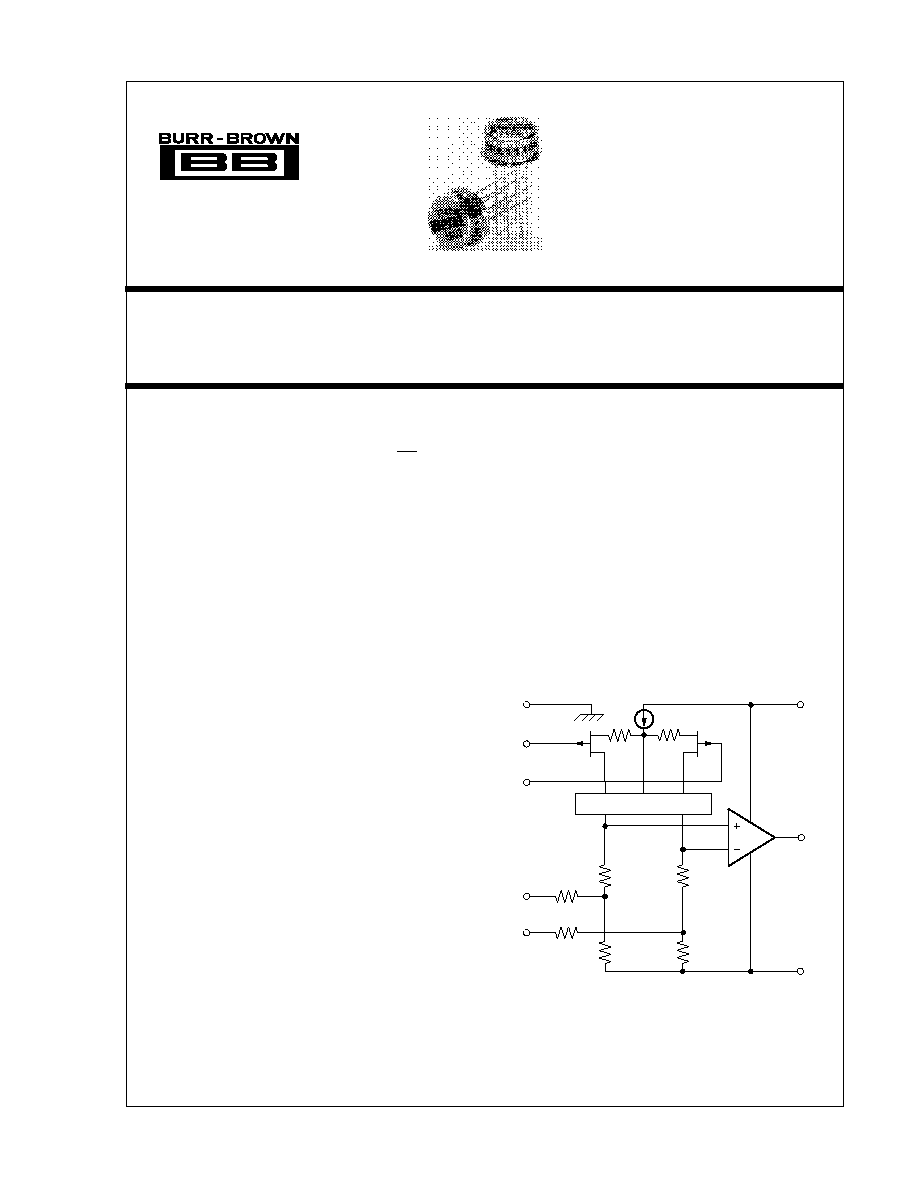
OPA111
Æ
8
2
3
1
5
7
6
4
Case and
Substrate
Output
Trim
+V
CC
Noise-Free Cascode
*
Trim
+In
≠In
≠V
CC
10k
10k
*Patented
2k
2k
2k
2k
DESCRIPTION
The OPA111 is a precision monolithic dielectrically
isolated FET (
Difet
Æ
) operational amplifier. Outstand-
ing performance characteristics allow its use in the
most critical instrumentation applications.
Noise, bias current, voltage offset, drift, open-loop
gain, common-mode rejection, and power supply re-
jection are superior to BIFET
Æ
amplifiers.
Very low bias current is obtained by dielectric isola-
tion with on-chip guarding.
Laser trimming of thin-film resistors gives very low
offset and drift. Extremely low noise is achieved with
patented circuit design techniques. A new cascode
design allows high precision input specifications and
reduced susceptibility to flicker noise.
Standard 741 pin configuration allows upgrading of
existing designs to higher performance levels.
© 1984 Burr-Brown Corporation
PDS-526K
Printed in U.S.A. August, 1995
2
OPA111
Æ
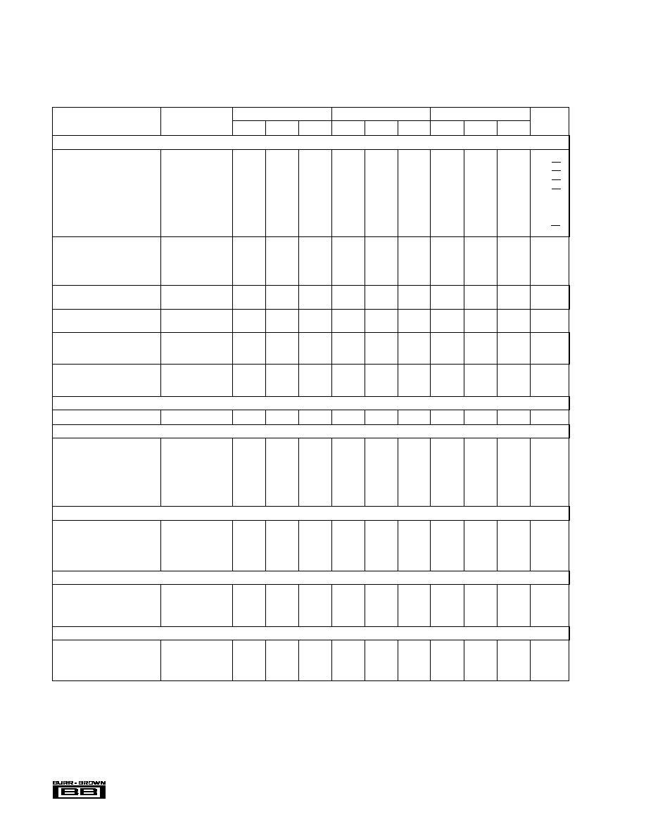
SPECIFICATIONS
ELECTRICAL
At V
CC
=
±
15VDC and T
A
= +25
∞
C unless otherwise noted.
OPA111AM
OPA111BM
OPA111SM
PARAMETER
CONDITION
MIN
TYP
MAX
MIN
TYP
MAX
MIN
TYP
MAX
UNITS
INPUT
NOISE
Voltage, f
O
= 10Hz
100% Tested
40
80
30
60
40
80
nV/
Hz
f
O
= 100Hz
100% Tested
15
40
11
30
15
40
nV/
Hz
f
O
= 1kHz
100% Tested
8
15
7
12
8
15
nV/
Hz
f
O
= 10kHz
100% Tested
6
8
6
8
6
8
nV/
Hz
f
B
= 10Hz to 10kHz
100% Tested
0.7
1.2
0.6
1
0.7
1.2
µ
Vrms
f
B
= 0.1Hz to 10Hz
(1)
1.6
3.3
1.2
2.5
1.6
3.3
µ
Vp-p
Current, f
B
= 0.1Hz to 10Hz
(1)
9.5
15
7.5
12
9.5
15
fAp-p
f
O
= 0.1Hz thru 20kHz
(1)
0.5
0.8
0.4
0.6
0.5
0.8
fA/
Hz
OFFSET VOLTAGE
(2)
Input Offset Voltage
V
CM
= 0VDC
±
100
±
500
±
50
±
250
±
100
±
500
µ
V
Average Drift
T
A
= T
MIN
to T
MAX
±
2
±
5
±
0.5
±
1
±
2
±
5
µ
V/
∞
C
Supply Rejection
V
CC
=
±
10V to
±
18V
90
110
100
110
90
110
dB
±
3
±
31
±
3
±
10
±
3
±
31
µ
V/V
BIAS CURRENT
(2)
Input Bias Current
V
CM
= 0VDC
±
0.8
±
2
±
0.5
±
1
±
0.8
±
2
pA
OFFSET CURRENT
(2)
Input Offset Current
V
CM
= 0VDC
±
0.5
±
1.5
±
0.25
±
0.75
±
0.5
±
1.5
pA
IMPEDANCE
Differential
10
13
|| 1
10
13
|| 1
10
13
|| 1
|| pF
Common-Mode
10
14
|| 3
10
14
|| 3
10
14
|| 3
|| pF
VOLTAGE RANGE
Common-Mode Input Range
±
10
±
11
±
10
±
11
±
10
±
11
V
Common-Mode Rejection
V
IN
=
±
10VDC
90
110
100
110
90
110
dB
OPEN-LOOP GAIN, DC
Open-Loop Voltage Gain
R
L
2k
114
125
120
125
114
125
dB
FREQUENCY RESPONSE
Unity Gain, Small Signal
2
2
2
MHz
Full Power Response
20Vp-p, R
L
= 2k
16
32
16
32
16
32
kHz
Slew Rate
V
O
=
±
10V, R
L
= 2k
1
2
1
2
1
2
V/
µ
s
Settling Time, 0.1%
Gain = ≠1, R
L
= 2k
6
6
6
µ
s
0.01%
10V Step
10
10
10
µ
s
Overload Recovery,
50% Overdrive
(3)
Gain = ≠1
5
5
5
µ
s
RATED OUTPUT
Voltage Output
R
L
= 2k
±
11
±
12
±
11
±
12
±
11
±
12
V
Current Output
V
O
=
±
10VDC
±
5.5
±
10
±
5.5
±
10
±
5.5
±
10
mA
Output Resistance
DC, Open Loop
100
100
100
Load Capacitance Stability
Gain = +1
1000
1000
1000
pF
Short Circuit Current
10
40
10
40
10
40
mA
POWER SUPPLY
Rated Voltage
±
15
±
15
±
15
VDC
Voltage Range, Derated
Performance
±
5
±
18
±
5
±
18
±
5
±
18
VDC
Current, Quiescent
I
O
= 0mADC
2.5
3.5
2.5
3.5
2.5
3.5
mA
TEMPERATURE RANGE
Specification
Ambient Temp.
≠25
+85
≠25
+85
≠55
+125
∞
C
Operating
Ambient Temp.
≠55
+125
≠55
+125
≠55
+125
∞
C
Storage
Ambient Temp.
≠65
+150
≠65
+150
≠65
+150
∞
C
Junction-Ambient
200
200
200
∞
C/W
NOTES: (1) Sample tested--this parameter is guaranteed. (2) Offset voltage, offset current, and bias current are measured with the units fully warmed up. (3) Overload
recovery is defined as the time required for the output to return from saturation to linear operation following the removal of a 50% input overdrive.
The information provided herein is believed to be reliable; however, BURR-BROWN assumes no responsibility for inaccuracies or omissions. BURR-BROWN assumes
no responsibility for the use of this information, and all use of such information shall be entirely at the user's own risk. Prices and specifications are subject to change without
notice. No patent rights or licenses to any of the circuits described herein are implied or granted to any third party. BURR-BROWN does not authorize or warrant any BURR-
BROWN product for use in life support devices and/or systems.

3
Æ
OPA111
ABSOLUTE MAXIMUM RATINGS
Supply ...........................................................................................
±
18VDC
Internal Power Dissipation
(1)
......................................................... 750mW
Differential Input Voltage
(2)
..........................................................
±
36VDC
Input Voltage Range
(2)
................................................................
±
18VDC
Storage Temperature Range ......................................... ≠65
∞
C to +150
∞
C
Operating Temperature Range ..................................... ≠55
∞
C to +125
∞
C
Lead Temperature (soldering, 10s) ............................................... +300
∞
C
Output Short Circuit Duration
(3)
.............................................. Continuous
Junction Temperature .................................................................... +175
∞
C
NOTES: (1) Packages must be derated based on
JC
= 150
∞
C/W or
JA
= 300
∞
C/W. (2) For supply voltages less than
±
18VDC, the absolute
maximum input voltage is equal to +18V > V
IN
> ≠V
CC
≠ 6V. See Figure
2. (3) Short circuit may be to power supply common only. Rating applies
to +25
∞
C ambient. Observe dissipation limit and T
J
.
ELECTRICAL (FULL TEMPERATURE RANGE SPECIFICATIONS)
At V
CC
=
±
15VDC and T
A
= T
MIN
to T
MAX
unless otherwise noted.
OPA111AM
OPA111BM
OPA111SM
PARAMETER
CONDITION
MIN
TYP
MAX
MIN
TYP
MAX
MIN
TYP
MAX
UNITS
TEMPERATURE RANGE
Specification Range
Ambient Temp.
≠25
+85
≠25
+85
≠55
+125
∞
C
INPUT
OFFSET VOLTAGE
(1)
Input Offset Voltage
V
CM
= 0VDC
±
220
±
1000
±
110
±
500
±
300
±
1500
µ
V
Average Drift
±
2
±
5
±
0.5
±
1
±
2
±
5
µ
V/
∞
C
Supply Rejection
V
CC
=
±
10V to
±
18V
86
100
90
100
86
100
dB
±
10
±
50
±
10
±
32
±
10
±
50
µ
V/V
BIAS CURRENT
(1)
Input Bias Current
V
CM
= 0VDC
±
50
±
250
±
30
±
130
±
820
±
4100
pA
OFFSET CURRENT
(1)
Input Offset Current
V
CM
= 0VDC
±
30
±
200
±
15
±
100
±
510
±
3100
pA
VOLTAGE RANGE
Common-Mode Input Range
±
10
±
11
±
10
±
11
±
10
±
11
V
Common-Mode Rejection
V
IN
=
±
10VDC
86
100
90
100
86
100
dB
OPEN-LOOP GAIN, DC
Open-Loop Voltage Gain
R
L
2k
110
120
114
120
110
120
dB
RATED OUTPUT
Voltage Output
R
L
= 2k
±
10.5
±
11
±
11
±
11.5
±
11
±
11.5
V
Current Output
V
O
=
±
10VDC
±
5.25
±
10
±
5.25
±
10
±
5.25
±
10
mA
Short Circuit Current
V
O
= 0VDC
10
40
10
40
10
40
mA
POWER SUPPLY
Current, Quiescent
I
O
= 0mADC
2.5
3.5
2.5
3.5
2.5
3.5
mA
NOTES: (1) Offset voltage, offset current, and bias current are measured with the units fully warmed up.
ORDERING INFORMATION
OFFSET
TEMPERATURE
VOLTAGE,
MODEL
PACKAGE
RANGE
MAX (
µ
V)
OPA111AM
TO-99
≠25
∞
C to +85
∞
C
±
500
OPA111BM
TO-99
≠25
∞
C to +85
∞
C
±
250
OPA111SM
TO-99
≠55
∞
C to +125
∞
C
±
500
CONNECTION DIAGRAM
Top View
OPA111
8
1
2
7
6
5
3
4
Offset
Trim
Offset
Trim
Output
+V
CC
Substrate and Case
≠V
CC
≠In
+In
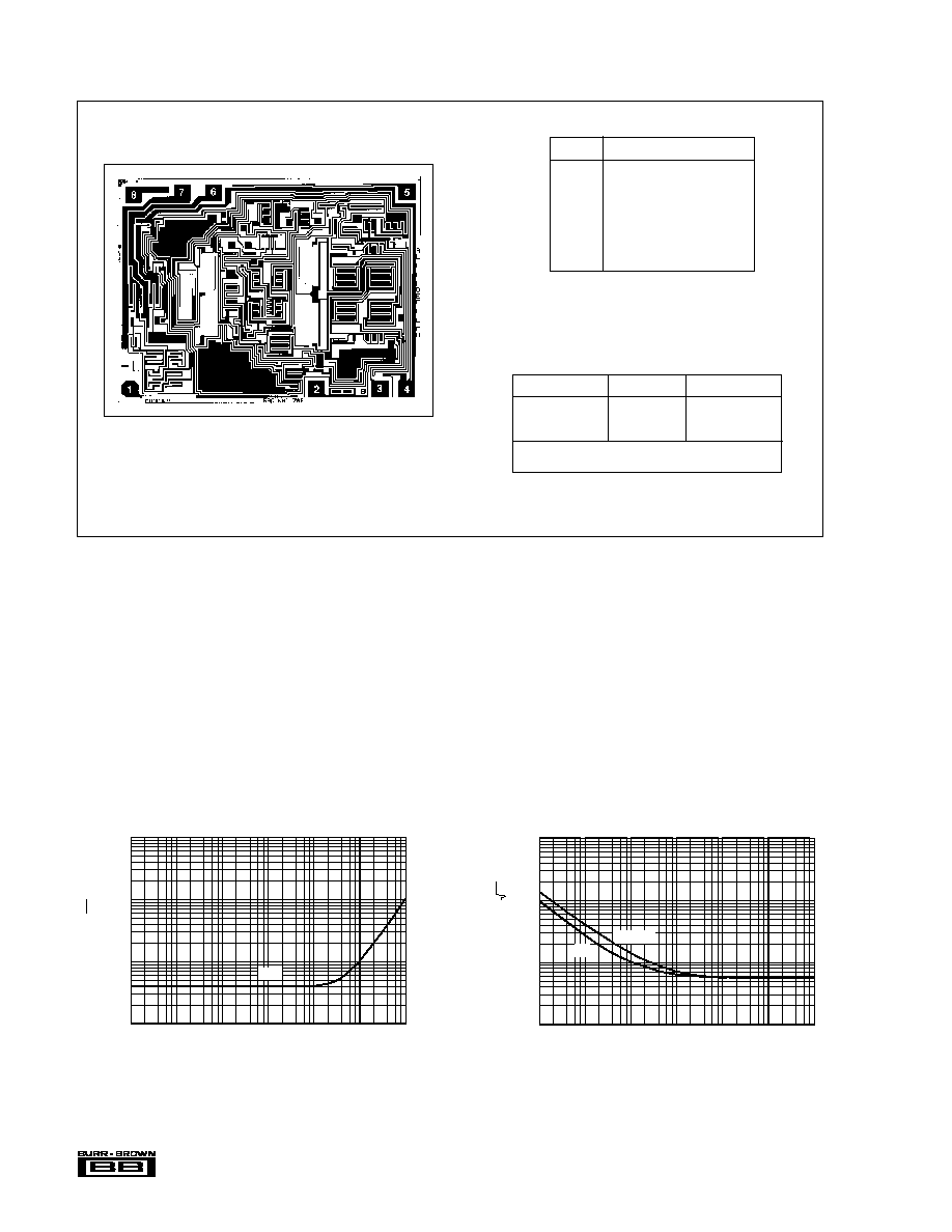
PACKAGE INFORMATION
PACKAGE DRAWING
MODEL
PACKAGE
NUMBER
(1)
OPA111AM
TO-99
001
OPA111BM
TO-99
001
OPA111SM
TO-99
001
NOTE: (1) For detailed drawing and dimension table, please see end of data
sheet, or Appendix D of Burr-Brown IC Data Book.
4
OPA111
Æ
DICE INFORMATION
OPA111AD DIE TOPOGRAPHY
PAD
FUNCTION
1
Offset Trim
2
≠In
3
+In
4
≠V
S
5
Offset Trim
6
Output
7
+V
S
8
Substrate
Substrate Bias: This Dielectrically-Isolated
Substrate is normally connected to common.
MECHANICAL INFORMATION
MILS (0.001")
MILLIMETERS
Die Size
95 x 71
±
5
2.41 x 1.80
±
0.13
Die Thickness
20
±
3
0.51
±
0.08
Min. Pad Size
4 x 4
0.10 x 0.10
Backing:
None
Transistor Count:
44
TYPICAL PERFORMANCE CURVES
T
A
= +25
∞
C, V
CC
=
±
15VDC unless otherwise noted.
INPUT CURRENT NOISE SPECTRAL DENSITY
1k
Frequency (Hz)
100
10
1
10k
100k
1M
100
10
1
0.1
Current Noise (fA/
Hz
BM
INPUT VOLTAGE NOISE SPECTRAL DENSITY
1k
Frequency (Hz)
10k
100k
1M
100
10
1
1k
100
10
1
Voltage Noise (nV/
Hz)
BM
AM, SM
5
Æ
OPA111
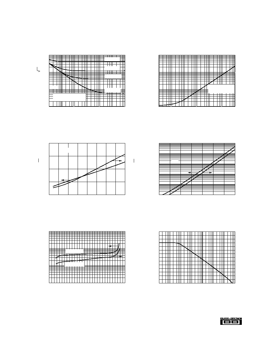
TYPICAL PERFORMANCE CURVES
(CONT)
T
A
= +25
∞
C, V
CC
=
±
15VDC unless otherwise noted.
TOTAL* INPUT VOLTAGE NOISE SPECTRAL
DENSITY vs SOURCE RESISTANCE
100
Frequency (Hz)
1k
10k
100k
10
1
0.1
1k
100
10
1
Voltage Noise (nV/
Hz)
R
S
= 10M
R
S
= 1M
R
S
= 100k
R
S
= 100
BM
*Includes contribution
from source resistance.
TOTAL* INPUT VOLTAGE NOISE (PEAK-TO-PEAK)
vs SOURCE RESISTANCE
10
4
10
5
10
6
10
7
10
8
10
9
10
10
1k
100
10
1
Voltage Noise (µVp-p)
*Includes contribution
from source resistance.
Source Resistance (
)
BM
f
B
= 0.1Hz to 10Hz
VOLTAGE AND CURRENT NOISE SPECTRAL
DENSITY vs TEMPERATURE
12
10
8
6
4
≠50
≠25
0
25
50
75
100
125
Temperature (∞C)
≠75
100
10
1
0.1
0.01
f
O
= 1kHz
Current Noise (fA/
Hz)
Voltage Noise (nV/
Hz)
BIAS AND OFFSET CURRENT
vs TEMPERATURE
≠50
Ambient Temperature (∞C)
≠25
0
25
50
75
100
125
1k
100
10
1
0.1
0.01
Bias Current (pA)
BM
1k
100
10
1
0.1
0.01
Offset Current (pA)
BIAS AND OFFSET CURRENT
vs INPUT COMMON-MODE VOLTAGE
≠15
≠10
≠5
0
5
10
15
10
1
0.1
0.01
Bias Current (pA)
10
1
0.1
0.01
Offset Current (pA)
Common-Mode Voltage (V)
Bias Current
Offset Current
POWER SUPPLY REJECTION
vs FREQUENCY
1
Frequency (Hz)
10
100
1k
10k
100k
1M
10M
Power Supply Rejection (dB)
140
120
100
80
60
40
20
0