 | –≠–ª–µ–∫—Ç—Ä–æ–Ω–Ω—ã–π –∫–æ–º–ø–æ–Ω–µ–Ω—Ç: OPA129UB | –°–∫–∞—á–∞—Ç—å:  PDF PDF  ZIP ZIP |

Ultra-Low Bias Current
Difet
Æ
OPERATIONAL AMPLIFIER
FEATURES
q
ULTRA-LOW BIAS CURRENT: 100fA max
q
LOW OFFSET: 2mV max
q
LOW DRIFT: 10
µ
V/
∞
C max
q
HIGH OPEN-LOOP GAIN: 94dB min
q
LOW NOISE: 15nV/
Hz at 10kHz
q
PLASTIC DIP and SOIC PACKAGE
APPLICATIONS
q
PHOTODETECTOR PREAMP
q
CHROMATOGRAPHY
q
ELECTROMETER AMPLIFIERS
q
MASS SPECTROMETER
q
pH PROBE AMPLIFIER
q
ION GAGE MEASUREMENT
DESCRIPTION
The OPA129 is an ultra-low bias current mono-
lithic operational amplifier offered in an 8-pin PDIP
and SO-8 package. Using advanced geometry
dielectrically-isolated FET (
Difet
Æ
) inputs, this mono-
lithic amplifier achieves a high performance level.
Difet
fabrication eliminates isolation-junction leakage
current--the main contributor to input bias current
with conventional monolithic FETs. This reduces
input bias current by a factor of 10 to 100. Very low
input bias current can be achieved without resorting to
small-geometry FETs or CMOS designs which can
suffer from much larger offset voltage, voltage noise,
drift, and poor power supply rejection.
The OPA129's special pinout eliminates leakage cur-
rent that occurs with other op amps. Pins 1 and 4 have
no internal connection, allowing circuit board guard
traces--even with the surface-mount package version.
OPA129 is available in 8-pin DIP and SO-8 packages,
specified for operation from ≠40
∞
C to +85
∞
C.
OPA129
Difet
Æ
Burr-Brown Corp.
+In
Output
6
Noise-Free
Cascode
7
5
V≠
V+
30k
30k
≠In
3
2
Simplified Circuit
8
Substrate
Æ
International Airport Industrial Park ∑ Mailing Address: PO Box 11400 ∑ Tucson, AZ 85734 ∑ Street Address: 6730 S. Tucson Blvd. ∑ Tucson, AZ 85706
Tel: (520) 746-1111 ∑ Twx: 910-952-1111 ∑ Cable: BBRCORP ∑ Telex: 066-6491 ∑ FAX: (520) 889-1510 ∑ Immediate Product Info: (800) 548-6132
©
1994 Burr-Brown Corporation
PDS-1195A
Printed in U.S.A. July, 1994

Æ
OPA129
2
SPECIFICATIONS
ELECTRICAL
At V
S
=
±
15V and T
A
= +25
∞
C unless otherwise noted. Pin 8 connected to ground.
NOTES: (1) High-speed automated test. (2) Overload recovery is defined as the time required for the output to return from saturation to linear operation following the
removal of a 50% input overdrive.
The information provided herein is believed to be reliable; however, BURR-BROWN assumes no responsibility for inaccuracies or omissions. BURR-BROWN
assumes no responsibility for the use of this information, and all use of such information shall be entirely at the user's own risk. Prices and specifications are subject
to change without notice. No patent rights or licenses to any of the circuits described herein are implied or granted to any third party. BURR-BROWN does not
authorize or warrant any BURR-BROWN product for use in life support devices and/or systems.
OPA129PB, UB
OPA129P, U
PARAMETER
CONDITION
MIN
TYP
MAX
MIN
TYP
MAX
UNITS
INPUT BIAS CURRENT
(1)
V
CM
= 0V
±
30
±
100
*
±
250
fA
vs Temperature
Doubles every 10
∞
C
*
INPUT OFFSET CURRENT
V
CM
= 0V
±
30
*
fA
OFFSET VOLTAGE
Input Offset Voltage
V
CM
= 0V
±
0.5
±
2
±
1
±
5
mV
vs Temperature
±
3
±
10
±
5
µ
V/
∞
C
Supply Rejection
V
S
=
±
5V to
±
18V
±
3
±
100
*
*
µ
V/V
NOISE
Voltage
f = 10Hz
85
*
nV/
Hz
f = 100Hz
28
*
nV/
Hz
f = 1kHz
17
*
nV/
Hz
f = 10kHz
15
*
nV/
Hz
f
B
= 0.1Hz to 10Hz
4
*
µ
Vp-p
Current
f = 10kHz
0.1
*
fA/
Hz
INPUT IMPEDANCE
Differential
10
13
|| 1
*
|| pF
Common-Mode
10
15
|| 2
*
|| pF
VOLTAGE RANGE
Common-Mode Input Range
±
10
±
12
*
*
V
Common-Mode Rejection
V
IN
=
±
10V
80
118
*
*
dB
OPEN-LOOP GAIN, DC
Open-Loop Voltage Gain
R
L
2k
94
120
*
*
dB
FREQUENCY RESPONSE
Unity Gain, Small Signal
1
*
MHz
Full Power Response
20Vp-p, R
L
= 2k
47
*
kHz
Slew Rate
V
O
=
±
10V, R
L
= 2k
1
2.5
*
*
V/
µ
s
Settling Time:
G = ≠1, R
L
= 2k
,
10V Step
0.1%
5
*
µ
s
0.01%
10
*
µ
s
Overload Recovery, 50% Overdrive
(2)
G = ≠1
5
*
µ
s
RATED OUTPUT
Voltage Output
R
L
= 2k
±
12
±
13
*
*
V
Current Output
V
O
=
±
12V
±
6
±
10
*
*
mA
Load Capacitance Stability
Gain = +1
1000
*
pF
Short-Circuit Current
±
35
±
55
*
*
mA
POWER SUPPLY
Rated Voltage
±
15
*
V
Voltage Range, Derated Performance
±
5
±
18
*
*
V
Current, Quiescent
I
O
= 0mA
1.2
1.8
*
*
mA
TEMPERATURE
Specification
Ambient Temperature
≠40
+85
*
*
∞
C
Operating
Ambient Temperature
≠40
+125
*
*
∞
C
Storage
≠40
+125
*
*
∞
C
Thermal Resistance
JA
, Junction-to-Ambient
PDIP--"P"
90
*
∞
C/W
SOIC--"U"
100
*
∞
C/W

Æ
OPA129
3
100
1
1M
10M
1k
10k
100k
10
POWER SUPPLY REJECTION vs FREQUENCY
Frequency (Hz)
Power Supply Rejection (dB)
140
120
100
80
60
40
20
0
+PSRR
≠PSRR
OPEN-LOOP FREQUENCY RESPONSE
Frequency (Hz)
Voltage Gain (dB)
140
120
100
80
60
40
20
0
100
1
1M
10M
45
90
135
180
Pulse Shift (degrees)
Gain
1k
10k
100k
10
Phase
Margin
90∞
Power Supply Voltage ......................................................................
±
18V
Differential Input Voltage ............................................................ V≠ to V+
Input Voltage Range .................................................................... V≠ to V+
Storage Temperature Range ......................................... ≠40
∞
C to +125
∞
C
Operating Temperature Range ..................................... ≠40
∞
C to +125
∞
C
Lead Temperature (soldering, 10s; SOIC 3s) ............................... +300
∞
C
Output Short Circuit Duration
(1) ..................................................................
Continuous
Junction Temperature (T
J
) ............................................................. +150
∞
C
ABSOLUTE MAXIMUM RATINGS
NOTE: (1) Short circuit may be to power supply common at +25
∞
C ambient.
PACKAGE INFORMATION
PACKAGE DRAWING
MODEL
PACKAGE
NUMBER
(1)
OPA129P
8-pin Plastic DIP
006
OPA129PB
8-pin Plastic DIP
006
OPA129U
8-pin SOIC
182
OPA129UB
8-pin SOIC
182
NOTE: (1) For detailed drawing and dimension table, please see end of data
sheet, or Appendix D of Burr-Brown IC Data Book.
CONNECTION DIAGRAM
ELECTROSTATIC
DISCHARGE SENSITIVITY
Any integrated circuit can be damaged by ESD. Burr-Brown
recommends that all integrated circuits be handled with
appropriate precautions. Failure to observe proper handling
and installation procedures can cause damage.
ESD damage can range from subtle performance degrada-
tion to complete device failure. Precision integrated circuits
may be more susceptible to damage because very small
parametric changes could cause the device not to meet
published specifications.
Top View
DIP/SOIC
TYPICAL PERFORMANCE CURVES
T
A
= +25
∞
C, +15VDC, unless otherwise noted.
1
2
3
4
8
7
6
5
Substrate
V+
Output
V≠
NC
≠In
+In
NC
OPA
NC: No internal connection.
Æ
OPA129
4
0
Frequency (Hz)
FULL-POWER OUTPUT vs FREQUENCY
Output Voltage (Vp-p)
10k
100k
1k
1M
30
20
10
10
Frequency (Hz)
INPUT VOLTAGE NOISE SPECTRAL DENSITY
Voltage Density (nV/
Hz)
1
10
100
1k
10k
100k
1k
100
10
1
0.1
0.01
15
≠10
≠5
5
10
15
Common-Mode Voltage (V)
BIAS AND OFFSET CURRENT
vs INPUT COMMON-MODE VOLTAGE
Normalized Bias and Offset Current
0
BIAS AND OFFSET CURRENT vs TEMPERATURE
Ambient Temperature (∞C)
Bias and Offset Current (fA)
100pA
10pA
1pA
100
10
1
≠50
50
125
≠25
0
25
75
100
I
B
and I
OS
100
1
1M
10M
1k
10k
100k
10
COMMON-MODE REJECTION vs FREQUENCY
Frequency (Hz)
Common-Mode Rejection (dB)
140
120
100
80
60
40
20
0
COMMON-MODE REJECTION
vs INPUT COMMON-MODE VOLTAGE
Common-Mode Voltage (V)
Common-Mode Rejection (dB)
70
15
15
10
10
5
0
5
120
110
100
90
80
TYPICAL PERFORMANCE CURVES
(CONT)
T
A
= +25
∞
C, +15VDC, unless otherwise noted.

Æ
OPA129
5
OPEN-LOOP GAIN, PSR AND CMR vs TEMPERATURE
Ambient Temperature (∞C)
PSR, CMR, Voltage Gain (dB)
130
120
110
100
90
CMR
A
OL
PSR
≠75
125
≠50
75
≠25
0
25
50
100
SUPPLY CURRENT vs TEMPERATURE
Ambient Temperature (∞C)
Supply Current (mA)
2
1.5
1
0.5
0
≠75
125
≠50
75
≠25
0
25
50
100
0
Supply Voltage (±V
CC
)
GAIN BANDWIDTH AND SLEW RATE
vs SUPPLY VOLTAGE
Gain Bandwidth (MHz)
5
15
0
20
3
2
1
10
0
Slew Rate (v/µs)
6
4
2
+Slew
≠Slew
GBW
GAIN BANDWIDTH AND SLEW RATE
vs TEMPERATURE
Ambient Temperature (∞C)
Gain Bandwidth (MHz)
Slew Rate (V/µs)
4
3
2
1
4
3
2
1
0
0
≠75
125
≠50
75
≠25
0
25
50
100
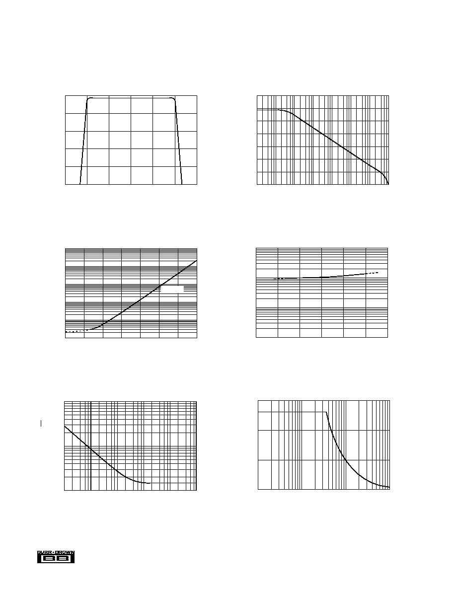
LARGE SIGNAL TRANSIENT RESPONSE
Time (µs)
Output Voltage (V)
10
0
≠10
0
50
25
TYPICAL PERFORMANCE CURVES
(CONT)
T
A
= +25
∞
C, +15VDC, unless otherwise noted.
SMALL SIGNAL TRANSIENT RESPONSE
Time (µs)
Output Voltage (mV)
80
40
0
≠40
0
10
2
4
6
8
≠80