 | –≠–ª–µ–∫—Ç—Ä–æ–Ω–Ω—ã–π –∫–æ–º–ø–æ–Ω–µ–Ω—Ç: OPA228 | –°–∫–∞—á–∞—Ç—å:  PDF PDF  ZIP ZIP |

Æ
High Precision, Low Noise
OPERATIONAL AMPLIFIERS
FEATURES
q
LOW NOISE: 3nV/
Hz
q
WIDE BANDWIDTH:
OPA227: 8MHz, 2.3V/
µ
s
OPA228: 33MHz, 10V/
µ
s
q
SETTLING TIME: 5
µ
s
(significant improvement over OP-27)
q
HIGH CMRR: 138dB
q
HIGH OPEN-LOOP GAIN: 160dB
q
LOW INPUT BIAS CURRENT: 10nA max
q
LOW OFFSET VOLTAGE: 75
µ
V max
q
WIDE SUPPLY RANGE:
±
2.5V to
±
18V
q
OPA227 REPLACES OP-27, LT1007, MAX427
q
OPA228 REPLACES OP-37, LT1037, MAX437
q
SINGLE, DUAL, AND QUAD VERSIONS
APPLICATIONS
q
DATA ACQUISITION
q
TELECOM EQUIPMENT
q
GEOPHYSICAL ANALYSIS
q
VIBRATION ANALYSIS
q
SPECTRAL ANALYSIS
q
PROFESSIONAL AUDIO EQUIPMENT
q
ACTIVE FILTERS
q
POWER SUPPLY CONTROL
OPA227
OPA2227
OPA4227
OPA228
OPA2228
OPA4228
© 1998 Burr-Brown Corporation
PDS-1494B
Printed in U.S.A. May, 1999
International Airport Industrial Park ∑ Mailing Address: PO Box 11400, Tucson, AZ 85734 ∑ Street Address: 6730 S. Tucson Blvd., Tucson, AZ 85706 ∑ Tel: (520) 746-1111
Twx: 910-952-1111 ∑ Internet: http://www.burr-brown.com/ ∑ Cable: BBRCORP ∑ Telex: 066-6491 ∑ FAX: (520) 889-1510 ∑ Immediate Product Info: (800) 548-6132
OPA4227
OPA227
OPA2
27
OPA2227
OPA4227
OPA2
227
For most current data sheet and other product
information, visit www.burr-brown.com
DESCRIPTION
The OPA227 and OPA228 series op amps combine
low noise and wide bandwidth with high precision to
make them the ideal choice for applications requiring
both ac and precision dc performance.
The OPA227 is unity gain stable and features high
slew rate (2.3V/
µ
s) and wide bandwidth (8MHz). The
OPA228 is optimized for closed-loop gains of 5 or
greater, and offers higher speed with a slew rate of
10V/
µ
s and a bandwidth of 33MHz.
The OPA227 and OPA228 series op amps are ideal
for professional audio equipment. In addition, low
quiescent current and low cost make them ideal for
portable applications requiring high precision.
The OPA227 and OPA228 series op amps are pin-
for-pin replacements for the industry standard OP-27
and OP-37 with substantial improvements across the
board. The dual and quad versions are available for
space savings and per-channel cost reduction.
The OPA227, OPA228, OPA2227, and OPA2228
are available in DIP-8 and SO-8 packages. The
OPA4227 and OPA4228 are available in DIP-14
and SO-14 packages with standard pin configura-
tions. Operation is specified from ≠40
∞
C to +85
∞
C.
SPICE Model available for OPA227 at www.burr-brown.com
1
2
3
4
8
7
6
5
Trim
V+
Output
NC
Trim
≠In
+In
V≠
OPA227, OPA228
DIP-8, SO-8
1
2
3
4
8
7
6
5
V+
Out B
≠In B
+In B
Out A
≠In A
+In A
V≠
OPA2227, OPA2228
DIP-8, SO-8
A
B
1
2
3
4
5
6
7
14
13
12
11
10
9
8
Out D
≠In D
+In D
V≠
+In C
≠In C
Out C
Out A
≠In A
+In A
V+
+In B
≠In B
Out B
OPA4227, OPA4228
DIP-14, SO-14
A
D
B
C

2
Æ
OPA227, 2227, 4227
OPA228, 2228, 4228
SPECIFICATIONS: V
S
=
±
5V to
±
15V
OPA227 Series
At T
A
= +25
∞
C, and R
L
= 10k
, unless otherwise noted.
Boldface limits apply over the specified temperature range, T
A
= ≠40
∞
C to +85
∞
C.
OPA227PA, UA
OPA227P, U
OPA2227PA, UA
OPA2227P, U
OPA4227PA, UA
PARAMETER
CONDITION
MIN
TYP
MAX
MIN
TYP
MAX
UNITS
OFFSET VOLTAGE
Input Offset Voltage
V
OS
±
5
±
75
±
10
±
200
µ
V
O
T
A
= ≠40
∞
C to +85
∞
C
ver Temperature
±
100
±
200
µ
V
vs Temperature
dV
OS
/dT
±
0.1
±
0.6
±
0.3
±
2
µ
V/
∞
C
vs Power Supply
PSRR
V
S
=
±
2.5V to
±
18V
±
0.5
±
2
T
T
µ
V/V
T
A
= ≠40
∞
C to +85
∞
C
±
2
T
µ
V/V
vs Time
0.2
T
µ
V/mo
Channel Separation (dual, quad)
dc
0.2
T
µ
V/V
f = 1kHz, R
L
= 5k
110
T
dB
INPUT BIAS CURRENT
Input Bias Current
I
B
±
2.5
±
10
T
T
nA
T
A
= ≠40
∞
C to +85
∞
C
±
10
T
nA
Input Offset Current
I
OS
±
2.5
±
10
T
T
nA
T
A
= ≠40
∞
C to +85
∞
C
±
10
T
nA
NOISE
Input Voltage Noise, f = 0.1Hz to 10Hz
90
T
nVp-p
15
T
nVrms
Input Voltage Noise Density, f = 10Hz e
n
3.5
T
nV/
Hz
f = 100Hz
3
T
nV/
Hz
f = 1kHz
3
T
nV/
Hz
Current Noise Density, f = 1kHz
i
n
0.4
T
pA/
Hz
INPUT VOLTAGE RANGE
Common-Mode Voltage Range
V
CM
(V≠)+2
(V+)≠2
T
T
V
Common-Mode Rejection
CMRR
V
CM
= (V≠)+2V
to (V+)≠2V
120
138
T
T
dB
T
A
= ≠40
∞
C to +85
∞
C
120
T
dB
INPUT IMPEDANCE
Differential
10
7
|| 12
T
|| pF
Common-Mode
V
CM
= (V≠)+2V
to (V+)≠2V
10
9
|| 3
T
|| pF
OPEN-LOOP GAIN
Open-Loop Voltage Gain
A
OL
V
O
= (V≠)+2V to (V+)≠2V, R
L
= 10k
132
160
T
T
dB
T
A
= ≠40
∞
C to +85
∞
C
132
T
dB
V
O
= (V≠)+3.5V to (V+)≠3.5V, R
L
= 600
132
160
T
T
dB
T
A
= ≠40
∞
C to +85
∞
C
132
T
dB
FREQUENCY RESPONSE
Gain Bandwidth Product
GBW
8
T
MHz
Slew Rate
SR
2.3
T
V/
µ
s
Settling Time: 0.1%
G = 1, 10V Step, C
L
= 100pF
5
T
µ
s
0.01%
G = 1, 10V Step, C
L
= 100pF
5.6
T
µ
s
Overload Recovery Time
V
IN
∑ G = V
S
1.3
T
µ
s
Total Harmonic Distortion + Noise THD+N
f = 1kHz, G = 1, V
O
= 3.5Vrms
0.00005
T
%
OUTPUT
Voltage Output
R
L
= 10k
(V≠)+2
(V+)≠2
T
T
V
T
A
= ≠40
∞
C to +85
∞
C
R
L
= 10k
(V≠)+2
(V+)≠2
T
T
V
R
L
= 600
(V≠)+3.5
(V+)≠3.5
T
T
V
T
A
= ≠40
∞
C to +85
∞
C
R
L
= 600
(V≠)+3.5
(V+)≠3.5
T
T
V
Short-Circuit Current
I
SC
±
45
T
mA
Capacitive Load Drive
C
LOAD
See Typical Curve
T
POWER SUPPLY
Specified Voltage Range
V
S
±
5
±
15
T
T
V
Operating Voltage Range
±
2.5
±
18
T
T
V
Quiescent Current (per amplifier)
I
Q
I
O
= 0
±
3.7
±
3.8
T
T
mA
T
A
= ≠40
∞
C to +85
∞
C
I
O
= 0
±
4.2
T
mA
TEMPERATURE RANGE
Specified Range
≠40
+85
T
T
∞
C
Operating Range
≠55
+125
T
T
∞
C
Storage Range
≠65
+150
T
T
∞
C
Thermal Resistance
JA
SO-8 Surface Mount
150
T
∞
C/W
DIP-8
100
T
∞
C/W
DIP-14
80
T
∞
C/W
SO-14 Surface Mount
100
T
∞
C/W
T
Specifications same as OPA227P, U.

3
Æ
OPA227, 2227, 4227
OPA228, 2228, 4228
OPA228PA, UA
OPA228P, U
OPA2228PA, UA
OPA2228P, U
OPA4228PA, UA
PARAMETER
CONDITION
MIN
TYP
MAX
MIN
TYP
MAX
UNITS
OFFSET VOLTAGE
Input Offset Voltage
V
OS
±
5
±
75
±
10
±
200
µ
V
O
T
A
= ≠40
∞
C to +85
∞
C
ver Temperature
±
100
±
200
µ
V
vs Temperature
dV
OS
/dT
±
0.1
±
0.6
±
0.3
±
2
µ
V/
∞
C
vs Power Supply
PSRR
V
S
=
±
2.5V to
±
18V
±
0.5
±
2
T
T
µ
V/V
T
A
= ≠40
∞
C to +85
∞
C
±
2
T
µ
V/V
vs Time
0.2
T
µ
V/mo
Channel Separation (dual, quad)
dc
0.2
T
µ
V/V
f = 1kHz, R
L
= 5k
110
T
dB
INPUT BIAS CURRENT
Input Bias Current
I
B
±
2.5
±
10
T
T
nA
T
A
= ≠40
∞
C to +85
∞
C
±
10
T
nA
Input Offset Current
I
OS
±
2.5
±
10
T
T
nA
T
A
= ≠40
∞
C to +85
∞
C
±
10
T
nA
NOISE
Input Voltage Noise, f = 0.1Hz to 10Hz
90
T
nVp-p
15
T
nVrms
Input Voltage Noise Density, f = 10Hz e
n
3.5
T
nV/
Hz
f = 100Hz
3
T
nV/
Hz
f = 1kHz
3
T
nV/
Hz
Current Noise Density, f = 1kHz
i
n
0.4
T
pA/
Hz
INPUT VOLTAGE RANGE
Common-Mode Voltage Range
V
CM
(V≠)+2
(V+)≠2
T
T
V
Common-Mode Rejection
CMRR
V
CM
= (V≠)+2V
to (V+)≠2V
120
138
T
T
dB
T
A
= ≠40
∞
C to +85
∞
C
120
T
dB
INPUT IMPEDANCE
Differential
10
7
|| 12
T
|| pF
Common-Mode
V
CM
= (V≠)+2V
to (V+)≠2V
10
9
|| 3
T
|| pF
OPEN-LOOP GAIN
Open-Loop Voltage Gain
A
OL
V
O
= (V≠)+2V to (V+)≠2V, R
L
= 10k
132
160
T
T
dB
T
A
= ≠40
∞
C to +85
∞
C
132
T
dB
V
O
= (V≠)+3.5V to (V+)≠3.5V, R
L
= 600
132
160
T
T
dB
T
A
= ≠40
∞
C to +85
∞
C
132
T
dB
FREQUENCY RESPONSE
Minimum Closed-Loop Gain
5
T
V/V
Gain Bandwidth Product
GBW
33
T
MHz
Slew Rate
SR
11
T
V/
µ
s
Settling Time: 0.1%
G = 5, 10V Step, C
L
= 100pF, C
F
=12pF
1.5
T
µ
s
0.01%
G = 5, 10V Step, C
L
= 100pF, C
F
=12pF
2
T
µ
s
Overload Recovery Time
V
IN
∑ G = V
S
0.6
T
µ
s
Total Harmonic Distortion + Noise THD+N
f = 1kHz, G = 5, V
O
= 3.5Vrms
0.00005
T
%
OUTPUT
Voltage Output
R
L
= 10k
(V≠)+2
(V+)≠2
T
T
V
T
A
= ≠40
∞
C to +85
∞
C
R
L
= 10k
(V≠)+2
(V+)≠2
T
T
V
R
L
= 600
(V≠)+3.5
(V+)≠3.5
T
T
V
T
A
= ≠40
∞
C to +85
∞
C
R
L
= 600
(V≠)+3.5
(V+)≠3.5
T
T
V
Short-Circuit Current
I
SC
±
45
T
mA
Capacitive Load Drive
C
LOAD
See Typical Curve
T
POWER SUPPLY
Specified Voltage Range
V
S
±
5
±
15
T
T
V
Operating Voltage Range
±
2.5
±
18
T
T
V
Quiescent Current (per amplifier)
I
Q
I
O
= 0
±
3.7
±
3.8
T
T
mA
T
A
= ≠40
∞
C to +85
∞
C
I
O
= 0
±
4.2
T
mA
TEMPERATURE RANGE
Specified Range
≠40
+85
T
T
∞
C
Operating Range
≠55
+125
T
T
∞
C
Storage Range
≠65
+150
T
T
∞
C
Thermal Resistance
JA
SO-8 Surface Mount
150
T
∞
C/W
DIP-8
100
T
∞
C/W
DIP-14
80
T
∞
C/W
SO-14 Surface Mount
100
T
∞
C/W
T
Specifications same as OPA228P, U.
SPECIFICATIONS: V
S
=
±
5V to
±
15V
OPA228 Series
At T
A
= +25
∞
C, and R
L
= 10k
, unless otherwise noted.
Boldface limits apply over the specified temperature range, T
A
= ≠40
∞
C to +85
∞
C.

4
Æ
OPA227, 2227, 4227
OPA228, 2228, 4228
ABSOLUTE MAXIMUM RATINGS
(1)
Supply Voltage ..................................................................................
±
18V
Signal Input Terminals, Voltage ........................ (V≠) ≠0.7V to (V+) +0.7V
Current ....................................................... 20mA
Output Short-Circuit
(2)
.............................................................. Continuous
Operating Temperature .................................................. ≠55
∞
C to +125
∞
C
Storage Temperature ..................................................... ≠65
∞
C to +150
∞
C
Junction Temperature ...................................................................... 150
∞
C
Lead Temperature (soldering, 10s) ................................................. 300
∞
C
NOTE: (1) Stresses above these ratings may cause permanent damage.
Exposure to absolute maximum conditions for extended periods may degrade
device reliability. (2) Short-circuit to ground, one amplifier per package.
ELECTROSTATIC
DISCHARGE SENSITIVITY
This integrated circuit can be damaged by ESD. Burr-Brown
recommends that all integrated circuits be handled with
appropriate precautions. Failure to observe proper handling
and installation procedures can cause damage.
ESD damage can range from subtle performance degrada-
tion to complete device failure. Precision integrated circuits
may be more susceptible to damage because very small
parametric changes could cause the device not to meet its
published specifications.
PACKAGE/ORDERING INFORMATION
The information provided herein is believed to be reliable; however, BURR-BROWN assumes no responsibility for inaccuracies or omissions. BURR-BROWN assumes
no responsibility for the use of this information, and all use of such information shall be entirely at the user's own risk. Prices and specifications are subject to change
without notice. No patent rights or licenses to any of the circuits described herein are implied or granted to any third party. BURR-BROWN does not authorize or warrant
any BURR-BROWN product for use in life support devices and/or systems.
OFFSET
OFFSET
PACKAGE
VOLTAGE
VOLTAGE DRIFT
DRAWING
TEMPERATURE
ORDERING
TRANSPORT
PRODUCT
max,
µ
V
max,
µ
V/
∞
C
PACKAGE
NUMBER
(1)
RANGE
NUMBER
(2)
MEDIA
OPA227 Series
Single
OPA227PA
±
200
±
2
DIP-8
006
≠40
∞
C to +85
∞
C
OPA227PA
Rails
OPA227P
±
75
±
0.6
DIP-8
006
≠40
∞
C to +85
∞
C
OPA227P
Rails
OPA227UA
±
200
±
2
SO-8 Surface Mount
182
≠40
∞
C to +85
∞
C
OPA227UA
Rails
"
"
"
"
"
"
OPA227UA/2K5
Tape and Reel
OPA227U
±
75
±
0.6
SO-8 Surface Mount
182
≠40
∞
C to +85
∞
C
OPA227U
Rails
"
"
"
"
"
"
OPA227U/2K5
Tape and Reel
Dual
OPA2227PA
±
200
±
2
DIP-8
006
≠40
∞
C to +85
∞
C
OPA2227PA
Rails
OPA2227P
±
75
±
0.6
DIP-8
006
≠40
∞
C to +85
∞
C
OPA2227P
Rails
OPA2227UA
±
200
±
2
SO-8 Surface Mount
182
≠40
∞
C to +85
∞
C
OPA2227UA
Rails
"
"
"
"
"
"
OPA2227UA/2K5
Tape and Reel
OPA2227U
±
75
±
0.6
SO-8 Surface Mount
182
≠40
∞
C to +85
∞
C
OPA2227U
Rails
"
"
"
"
"
"
OPA2227U/2K5
Tape and Reel
Quad
OPA4227PA
±
200
±
2
DIP-14
010
≠40
∞
C to +85
∞
C
OPA4227PA
Rails
OPA4227UA
±
200
±
2
SO-14 Surface Mount
235
≠40
∞
C to +85
∞
C
OPA4227UA
Rails
"
"
"
"
"
"
OPA4227UA/2K5
Tape and Reel
OPA228 Series
Single
OPA228PA
±
200
±
2
DIP-8
006
≠40
∞
C to +85
∞
C
OPA228PA
Rails
OPA228P
±
75
±
0.6
DIP-8
006
≠40
∞
C to +85
∞
C
OPA228P
Rails
OPA228UA
±
200
±
2
SO-8 Surface Mount
182
≠40
∞
C to +85
∞
C
OPA228UA
Rails
"
"
"
"
"
"
OPA228UA/2K5
Tape and Reel
OPA228U
±
75
±
0.6
SO-8 Surface Mount
182
≠40
∞
C to +85
∞
C
OPA228U
Rails
"
"
"
"
"
"
OPA228U/2K5
Tape and Reel
Dual
OPA2228PA
±
200
±
2
DIP-8
006
≠40
∞
C to +85
∞
C
OPA2228PA
Rails
OPA2228P
±
75
±
0.6
DIP-8
006
≠40
∞
C to +85
∞
C
OPA2228P
Rails
OPA2228UA
±
200
±
2
SO-8 Surface Mount
182
≠40
∞
C to +85
∞
C
OPA2228UA
Rails
"
"
"
"
"
"
OPA2228UA/2K5
Tape and Reel
OPA2228U
±
75
±
0.6
SO-8 Surface Mount
182
≠40
∞
C to +85
∞
C
OPA2228U
Rails
"
"
"
"
"
"
OPA2228U/2K5
Tape and Reel
Quad
OPA4228PA
±
200
±
2
DIP-14
010
≠40
∞
C to +85
∞
C
OPA4228PA
Rails
OPA4228UA
±
200
±
2
SO-14 Surface Mount
235
≠40
∞
C to +85
∞
C
OPA4228UA
Rails
"
"
"
"
"
"
OPA4228UA/2K5
Tape and Reel
NOTE: (1) For detailed drawing and dimension table, please see end of data sheet, or Appendix C of Burr-Brown IC Data Book. (2) Products followed by a slash
(/) are only available in Tape and Reel in the quantities indicated (e.g. /2K5 indicates 2500 devices per reel). Ordering 2500 pieces of "OPA227UA/2K5" will get
a single 2500 piece Tape and Reel. For detailed Tape and Reel mechanical information, refer to Appendix B of Burr-Brown IC Data Book.

5
Æ
OPA227, 2227, 4227
OPA228, 2228, 4228
TYPICAL PERFORMANCE CURVES
At T
A
= +25
∞
C, R
L
= 10k
, and V
S
=
±
15V, unless otherwise noted.
0.01 0.10
1
10
100
1k
10k 100k
1M 10M 100M
180
160
140
120
100
80
60
40
20
0
≠20
A
OL
(dB)
0
≠20
≠40
≠60
≠80
≠100
≠120
≠140
≠160
≠180
≠200
Phase (
∞
)
Frequency (Hz)
OPEN-LOOP GAIN/PHASE vs FREQUENCY
G
OPA228
20
100
1k
10k
20k
0.01
0.001
0.0001
0.00001
THD+Noise (%)
Frequency (Hz)
TOTAL HARMONIC DISTORTION + NOISE
vs FREQUENCY
G = 1, R
L
= 10k
V
OUT
= 3.5Vrms
OPA227
20
100
1k
10k
50k
0.01
0.001
0.0001
0.00001
THD+Noise (%)
Frequency (Hz)
TOTAL HARMONIC DISTORTION + NOISE
vs FREQUENCY
G = 1, R
L
= 10k
V
OUT
= 3.5Vrms
OPA228
0.01 0.10
1
10
100
1k
10k 100k
1M 10M 100M
180
160
140
120
100
80
60
40
20
0
≠20
A
OL
(dB)
0
≠20
≠40
≠60
≠80
≠100
≠120
≠140
≠160
≠180
≠200
Phase (
∞
)
Frequency (Hz)
OPEN-LOOP GAIN/PHASE vs FREQUENCY
G
OPA227
1
0.1
10
100
1k
10k
100k
1M
140
120
100
80
60
40
-20
≠0
PSRR, CMRR (dB)
Frequency (Hz)
POWER SUPPLY AND COMMON-MODE
REJECTION RATIO vs FREQUENCY
+CMRR
+PSRR
≠PSRR
0.1
10
1
100
1k
10k
100k
10k
1k
100
10
1
Voltage Noise (nV/
Hz)
Current Noise (fA/
Hz)
Frequency (Hz)
INPUT VOLTAGE AND CURRENT NOISE
SPECTRAL DENSITY vs FREQUENCY
Current Noise
Voltage Noise
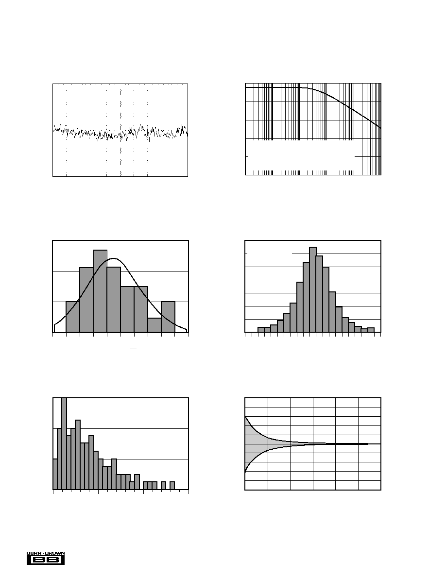
6
Æ
OPA227, 2227, 4227
OPA228, 2228, 4228
TYPICAL PERFORMANCE CURVES
(CONT)
At T
A
= +25
∞
C, R
L
=10k
, and V
S
=
±
15V, unless otherwise noted.
OFFSET VOLTAGE PRODUCTION DISTRIBUTION
Percent of Amplifiers (%)
Offset Voltage (
µ
V)
≠150
≠135
≠120
≠105
≠90
≠75
≠60
≠45
≠30
≠15
0
15
30
45
60
75
90
105
120
135
150
17.5
15.0
12.5
10.0
5.5
5.0
2.5
0
Typical distribution
of packaged units.
OFFSET VOLTAGE DRIFT PRODUCTION DISTRIBUTION
Percent of Amplifiers (%)
Offset Voltage Drift (
µ
V)/
∞
C
12
8
4
0
Typical distribution
of packaged units.
0
0.5
1.0
1.5
10
8
6
4
2
0
≠2
≠4
≠6
≠8
≠10
Offset Voltage Change (
µ
V)
0
100
150
300
Time from Power Supply Turn-On (s)
WARM-UP OFFSET VOLTAGE DRIFT
50
200
250
10
100
1k
10k
100k
1M
140
120
100
80
60
40
Channel Separation (dB)
Frequency (Hz)
CHANNEL SEPARATION vs FREQUENCY
Dual and quad devices. G = 1, all channels.
Quad measured Channel A to D, or B to C;
other combinations yield similiar or improved
rejection.
INPUT NOISE VOLTAGE vs TIME
1s/div
50nV/div
VOLTAGE NOISE DISTRIBUTION (10Hz)
Percent of Units (%)
Noise (nV/
Hz)
3.16
0
3.25
3.34 3.43
3.51 3.60
3.69 3.78
24
16
8
0

7
Æ
OPA227, 2227, 4227
OPA228, 2228, 4228
TYPICAL PERFORMANCE CURVES
(CONT)
At T
A
= +25
∞
C, R
L
= 10k
, and V
S
=
±
15V, unless otherwise noted.
≠60
≠40
≠20
0
20
40
60
80
100
120 140
2.0
1.5
1.0
0.5
0
≠0.5
≠1.0
≠1.5
≠2.0
Input Bias Current (nA)
Temperature (
∞
C)
INPUT BIAS CURRENT vs TEMPERATURE
≠75
≠50
≠25
0
25
50
75
100
125
60
50
40
30
20
10
0
Short-Circuit Current (mA)
Temperature (
∞
C)
SHORT-CIRCUIT CURRENT vs TEMPERATURE
+I
SC
≠I
SC
QUIESCENT CURRENT vs TEMPERATURE
100
120 140
Temperature (
∞
C)
≠60
≠40
≠20
0
20
40
60
80
5.0
4.5
4.0
3.5
3.0
2.5
Quiescent Current (mA)
±
10V
±
5V
±
2.5V
±
18V
±
15V
±
12V
QUIESCENT CURRENT vs SUPPLY VOLTAGE
20
Supply Voltage (
±
V)
0
2
4
6
8
10
12
14
16
18
3.8
3.6
3.4
3.2
3.0
2.8
Quiescent Current (mA)
≠75
≠50
≠25
0
25
50
75
100
125
160
150
140
130
120
110
100
90
80
70
60
A
OL
, CMRR, PSRR (dB)
Temperature (
∞
C)
A
OL
, CMRR, PSRR vs TEMPERATURE
CMRR
PSRR
A
OL
OPA227
≠75
≠50
≠25
0
25
50
75
100
125
160
150
140
130
120
110
100
90
80
70
60
A
OL
, CMRR, PSRR (dB)
Temperature (
∞
C)
A
OL
, CMRR, PSRR vs TEMPERATURE
CMRR
PSRR
A
OL
OPA228

8
Æ
OPA227, 2227, 4227
OPA228, 2228, 4228
TYPICAL PERFORMANCE CURVES
(CONT)
At T
A
= +25
∞
C, R
L
= 10k
, and V
S
=
±
15V, unless otherwise noted.
2.0
1.5
1.0
0.5
0
≠0.5
≠1.0
≠1.5
≠2.0
I
B
(nA)
0
5
10
15
20
25
30
35
40
Supply Voltage (V)
CHANGE IN INPUT BIAS CURRENT
vs POWER SUPPLY VOLTAGE
Curve shows normalized change in bias current
with respect to V
S
=
±
10V. Typical I
B
may range
from ≠2nA to +2nA at V
S
=
±
10V.
CHANGE IN INPUT BIAS CURRENT
vs COMMON-MODE VOLTAGE
15
Common-Mode Voltage (V)
≠15
≠10
≠5
0
5
10
1.5
1.0
0.5
0
≠0.5
≠1.0
≠1.5
I
B
(nA)
V
S
=
±
15V
V
S
=
±
5V
Curve shows normalized change in bias current
with respect to V
CM
= 0V. Typical I
B
may range
from ≠2nA to +2nA at V
CM
= 0V.
OUTPUT VOLTAGE SWING vs OUTPUT CURRENT
15
14
13
12
11
10
≠10
≠11
≠12
≠13
≠14
≠15
V+
(V+) ≠1V
(V+) ≠2V
(V+) ≠3V
(V≠) +3V
(V≠) +2V
(V≠) +1V
V≠
0
10
20
30
40
50
60
Output Current (mA)
Output Voltage Swing (V)
≠55
∞
C
≠40
∞
C
≠55
∞
C
85
∞
C
25
∞
C
85
∞
C
25
∞
C
≠40
∞
C
125
∞
C
125
∞
C
100
10
1
Settling Time (
µ
s)
±
1
±
10
±
100
Gain (V/V)
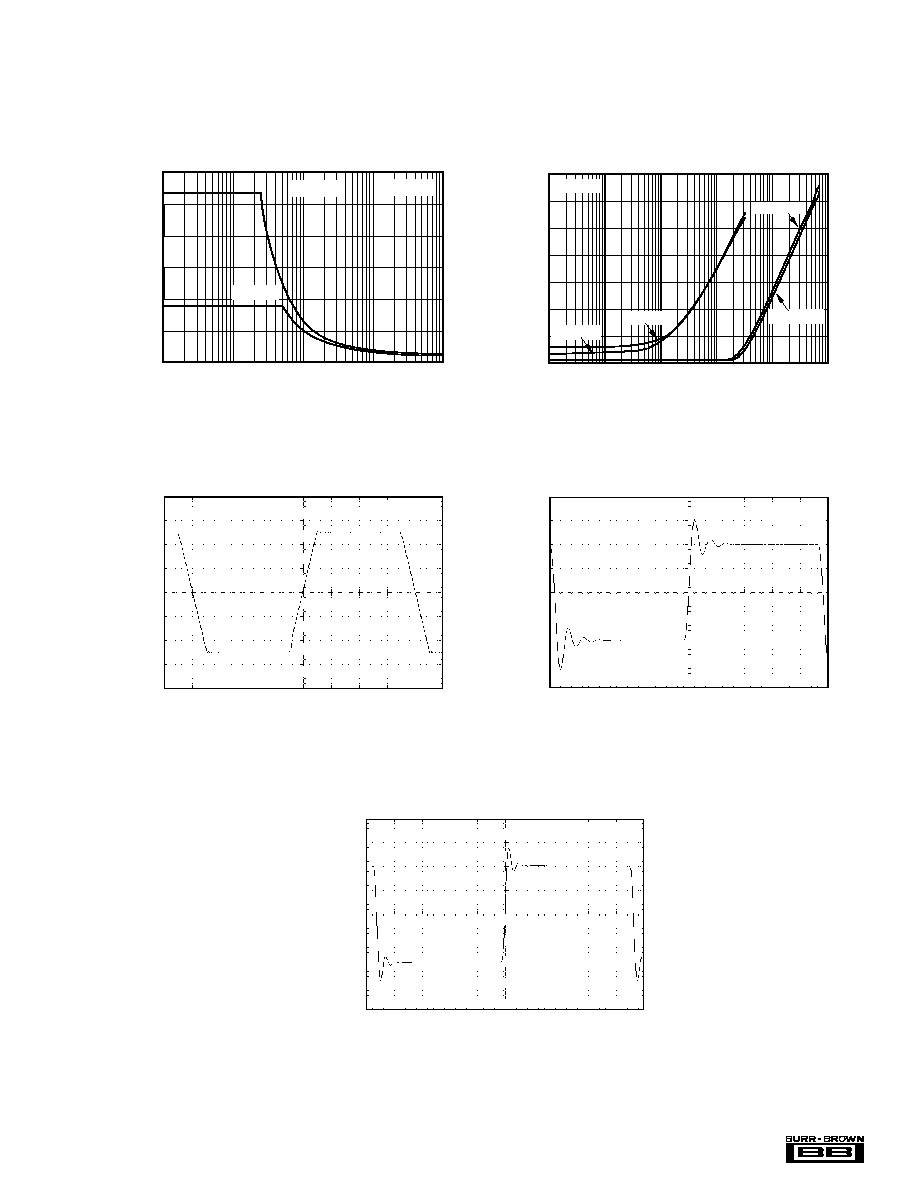
SETTLING TIME vs CLOSED-LOOP GAIN
0.01%
OPA227
0.1%
V
S
=
±
15V, 10V Step
C
L
= 1500pF
R
L
= 2k
0.01%
OPA228
0.1%
SLEW RATE vs TEMPERATURE
125
Temperature (
∞
C)
≠75
≠50
≠25
0
25
50
75
100
3.0
2.5
2.0
1.5
1.0
0.5
0
Slew Rate (
µ
V/V)
Negative Slew Rate
R
LOAD
= 2k
C
LOAD
= 100pF
Positive Slew Rate
OPA227
SLEW RATE vs TEMPERATURE
125
Temperature (
∞
C)
≠75
≠50
≠25
0
25
50
75
100
12
10
8
6
4
2
0
Slew Rate (
µ
V/V)
R
LOAD
= 2k
C
LOAD
= 100pF
OPA228
9
Æ
OPA227, 2227, 4227
OPA228, 2228, 4228
TYPICAL PERFORMANCE CURVES
(CONT)
At T
A
= +25
∞
C, R
L
= 10k
, and V
S
=
±
15V, unless otherwise noted.
LARGE-SIGNAL STEP RESPONSE
G = ≠1, C
L
= 1500pF
5
µ
s/div
2V/div
SMALL-SIGNAL STEP RESPONSE
G = +1, C
L
= 1000pF
400ns/div
25mV/div
SMALL-SIGNAL STEP RESPONSE
G = +1, C
L
= 5pF
400ns/div
25mV/div
SMALL-SIGNAL OVERSHOOT
vs LOAD CAPACITANCE
1k
100
10
1
10k
100k
Load Capacitance (pF)
70
60
50
40
30
20
10
0
Overshoot (%)
Gain = ≠10
Gain = +10
OPA227
Gain = +1
Gain = ≠1
OPA227
OPA227
OPA227
MAXIMUM OUTPUT VOLTAGE vs FREQUENCY
10M
Frequency (Hz)
1k
10k
100k
1M
30
25
20
15
10
5
0
Output Voltage (Vp-p)
V
S
=
±
15V
OPA227
V
S
=
±
5V
10
Æ
OPA227, 2227, 4227
OPA228, 2228, 4228
TYPICAL PERFORMANCE CURVES
(CONT)
At T
A
= +25
∞
C, R
L
= 10k
, and V
S
=
±
15V, unless otherwise noted.
SMALL-SIGNAL STEP RESPONSE
G = +10, C
L
= 1000pF, R
L
= 1.8k
500ns/div
200mV/div
SMALL-SIGNAL STEP RESPONSE
G = +10, C
L
= 5pF, R
L
= 1.8k
500ns/div
200mV/div
LARGE-SIGNAL STEP RESPONSE
G = ≠10, C
L
= 100pF
2
µ
s/div
5V/div
SMALL-SIGNAL OVERSHOOT
vs LOAD CAPACITANCE
1k
100
10
1
100k
10k
Load Capacitance (pF)
70
60
50
40
30
20
10
0
Overshoot (%)
G = ≠100
G = +100
OPA228
G =
±
10
OPA228
OPA228
OPA228
MAXIMUM OUTPUT VOLTAGE vs FREQUENCY
1M
10M
Frequency (Hz)
1k
10k
100k
30
25
20
15
10
5
0
Output Voltage (Vp-p)
V
S
=
±
15V
V
S
=
±
5V
OPA228

11
Æ
OPA227, 2227, 4227
OPA228, 2228, 4228
FIGURE 1. OPA227 Offset Voltage Trim Circuit.
APPLICATIONS INFORMATION
The OPA227 and OPA228 series are precision op amps with
very low noise. The OPA227 series is unity-gain stable with
a slew rate of 2.3V/
µ
s and 8MHz bandwidth. The OPA228
series is optimized for higher-speed applications with gains
of 5 or greater, featuring a slew rate of 10V/
µ
s and 33MHz
bandwidth. Applications with noisy or high impedance
power supplies may require decoupling capacitors close to
the device pins. In most cases, 0.1
µ
F capacitors are ad-
equate.
OFFSET VOLTAGE AND DRIFT
The OPA227 and OPA228 series have very low offset
voltage and drift. To achieve highest dc precision, circuit
layout and mechanical conditions should be optimized.
Connections of dissimilar metals can generate thermal po-
tentials at the op amp inputs which can degrade the offset
voltage and drift. These thermocouple effects can exceed
the inherent drift of the amplifier and ultimately degrade its
performance. The thermal potentials can be made to cancel
by assuring that they are equal at both input terminals. In
addition:
∑ Keep thermal mass of the connections made to the two
input terminals similar.
∑ Locate heat sources as far as possible from the critical
input circuitry.
∑ Shield op amp and input circuitry from air currents such
as those created by cooling fans.
OPERATING VOLTAGE
OPA227 and OPA228 series op amps operate from
±
2.5V to
±
18V supplies with excellent performance. Unlike most op
amps which are specified at only one supply voltage, the
OPA227 series is specified for real-world applications; a
single set of specifications applies over the
±
5V to
±
15V
supply range. Specifications are guaranteed for applications
between
±
5V and
±
15V power supplies. Some applications
do not require equal positive and negative output voltage
swing. Power supply voltages do not need to be equal. The
OPA227 and OPA228 series can operate with as little as 5V
between the supplies and with up to 36V between the
supplies. For example, the positive supply could be set to
25V with the negative supply at ≠5V or vice-versa. In
addition, key parameters are guaranteed over the specified
temperature range, ≠40
∞
C to +85
∞
C. Parameters which vary
significantly with operating voltage or temperature are shown
in the Typical Performance Curves.
OFFSET VOLTAGE ADJUSTMENT
The OPA227 and OPA228 series are laser-trimmed for
very low offset and drift so most applications will not
require external adjustment. However, the OPA227 and
OPA228 (single versions) provide offset voltage trim con-
nections on pins 1 and 8. Offset voltage can be adjusted by
connecting a potentiometer as shown in Figure 1. This
adjustment should be used only to null the offset of the op
amp. This adjustment should not be used to compensate for
offsets created elsewhere in the system since this can
introduce additional temperature drift.
INPUT PROTECTION
Back-to-back diodes (see Figure 2) are used for input protec-
tion on the OPA227 and OPA228. Exceeding the turn-on
threshold of these diodes, as in a pulse condition, can cause
current to flow through the input protection diodes due to the
amplifier's finite slew rate. Without external current-limiting
resistors, the input devices can be destroyed. Sources of high
input current can cause subtle damage to the amplifier.
Although the unit may still be functional, important param-
eters such as input offset voltage, drift, and noise may shift.
FIGURE 2. Pulsed Operation.
When using the OPA227 as a unity-gain buffer (follower), the
input current should be limited to 20mA. This can be accom-
plished by inserting a feedback resistor or a resistor in series
with the source. Sufficient resistor size can be calculated:
R
X
= V
S
/20mA ≠ R
SOURCE
where R
X
is either in series with the source or inserted in
the feedback path. For example, for a 10V pulse (V
S
=
10V), total loop resistance must be 500
. If the source
impedance is large enough to sufficiently limit the current
on its own, no additional resistors are needed. The size of
any external resistors must be carefully chosen since they
will increase noise. See the Noise Performance section of
this data sheet for further information on noise calcula-
tion. Figure 2 shows an example implementing a current-
limiting feedback resistor.
OPA227
20k
0.1
µ
F
0.1
µ
F
2
1
7
8
6
3
4
V+
V≠
Trim range exceeds
offset voltage specification
OPA227 and OPA228 single op amps only.
Use offset adjust pins only to
null offset voltage of op amp.
See text.
OPA227
Output
R
F
500
Input
≠
+

12
Æ
OPA227, 2227, 4227
OPA228, 2228, 4228
INPUT BIAS CURRENT CANCELLATION
The input bias current of the OPA227 and OPA228 series is
internally compensated with an equal and opposite cancella-
tion current. The resulting input bias current is the difference
between with input bias current and the cancellation current.
The residual input bias current can be positive or negative.
When the bias current is cancelled in this manner, the input
bias current and input offset current are approximately equal.
A resistor added to cancel the effect of the input bias current
(as shown in Figure 3) may actually increase offset and noise
and is therefore not recommended.
Design of low noise op amp circuits requires careful
consideration of a variety of possible noise contributors:
noise from the signal source, noise generated in the op
amp, and noise from the feedback network resistors. The
total noise of the circuit is the root-sum-square combina-
tion of all noise components.
The resistive portion of the source impedance produces
thermal noise proportional to the square root of the
resistance. This function is shown plotted in Figure 4.
Since the source impedance is usually fixed, select the op
amp and the feedback resistors to minimize their contri-
bution to the total noise.
Figure 4 shows total noise for varying source imped-
ances with the op amp in a unity-gain configuration (no
feedback resistor network and therefore no additional
noise contributions). The operational amplifier itself con-
tributes both a voltage noise component and a current
FIGURE 3. Input Bias Current Cancellation.
FIGURE 4. Noise Performance of the OPA227 in Unity-
Gain Buffer Configuration.
NOISE PERFORMANCE
Figure 4 shows total circuit noise for varying source imped-
ances with the op amp in a unity-gain configuration (no
feedback resistor network, therefore no additional noise con-
tributions). Two different op amps are shown with total circuit
noise calculated. The OPA227 has very low voltage noise,
making it ideal for low source impedances (less than 20k
).
A similar precision op amp, the OPA277, has somewhat higher
voltage noise but lower current noise. It provides excellent
noise performance at moderate source impedance (10k
to
100k
). Above 100k
, a FET-input op amp such as the
OPA132 (very low current noise) may provide improved
performance. The equation is shown for the calculation of the
total circuit noise. Note that e
n
= voltage noise, i
n
= current
noise, R
S
= source impedance, k = Boltzmann's constant =
1.38 ∑ 10
≠23
J/K and T is temperature in K. For more details on
calculating noise, see the insert titled "Basic Noise Calcula-
tions."
noise component. The voltage noise is commonly mod-
eled as a time-varying component of the offset voltage.
The current noise is modeled as the time-varying compo-
nent of the input bias current and reacts with the source
resistance to create a voltage component of noise. Conse-
quently, the lowest noise op amp for a given application
depends on the source impedance. For low source imped-
ance, current noise is negligible and voltage noise gener-
ally dominates. For high source impedance, current noise
may dominate.
Figure 5 shows both inverting and noninverting op amp
circuit configurations with gain. In circuit configurations
with gain, the feedback network resistors also contribute
noise. The current noise of the op amp reacts with the
feedback resistors to create additional noise components.
The feedback resistor values can generally be chosen to
make these noise sources negligible. The equations for
total noise are shown for both configurations.
BASIC NOISE CALCULATIONS
Op Amp
R
1
R
2
R
B
= R
2
|| R
1
External Cancellation Resistor
Not recommended
for OPA227
Conventional Op Amp Configuration
Recommended OPA227 Configuration
OPA227
R
1
R
2
No cancellation resistor.
See text.
VOLTAGE NOISE SPECTRAL DENSITY
vs SOURCE RESISTANCE
100k
10M
Source Resistance, R
S
(
)
100
1k
10k
1.00+03
1.00E+02
1.00E+01
1.00E+00
Votlage Noise Spectral Density, E
0
Typical at 1k (V/
Hz)
OPA227
OPA277
Resistor Noise
Resistor Noise
OPA277
OPA227
R
S
E
O
E
O
2
= e
n
2
+ (i
n
R
S
)
2
+ 4kTR
S

13
Æ
OPA227, 2227, 4227
OPA228, 2228, 4228
FIGURE 5. Noise Calculation in Gain Configurations.
Where e
S
=
4kTR
S
∑ = thermal noise of R
S
e
1
=
4kTR
1
∑ = thermal noise of R
1
e
2
=
4kTR
2
= thermal noise of R
2
1
2
1
+
R
R
Noise at the output:
R
R
2
1
E
R
R
e
e
e
i R
e
i R
R
R
O
n
n
S
n
S
2
2
1
2
2
1
2
2
2
2
2
2
2
2
1
2
1
1
= +
+
+
+
(
)
+
+
(
)
+
Where e
S
=
4kTR
S
∑
= thermal noise of R
S
e
1
=
4kTR
1
∑
= thermal noise of R
1
e
2
=
4kTR
2
= thermal noise of R
2
Noise at the output:
R
R
R
S
2
1
+
R
R
R
S
2
1
+
E
R
R
R
e
e
e
i R
e
O
S
n
n
S
2
2
1
2
2
1
2
2
2
2
2
2
1
= +
+
+
+
+
(
)
+
R
1
R
2
R
2
E
O
R
1
R
2
E
O
R
S
V
S
R
S
V
S
Noise in Noninverting Gain Configuration
Noise in Inverting Gain Configuration
For the OPA227 and OPA228 series op amps at 1kHz, e
n
= 3nV/
Hz and i
n
= 0.4pA/
Hz.

14
Æ
OPA227, 2227, 4227
OPA228, 2228, 4228
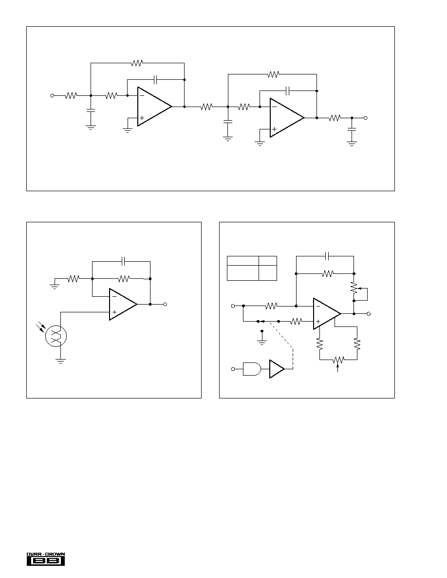
Figure 6 shows the 0.1Hz 10Hz bandpass filter used to test
the noise of the OPA227 and OPA228. The filter circuit was
designed using Burr-Brown's FilterPro software (available
at www.burr-brown.com). Figure 7 shows the configura-
tion of the OPA227 and OPA228 for noise testing.
FIGURE 6. 0.1Hz to 10Hz Bandpass Filter Used to Test Wideband Noise of the OPA227 and OPA228 Series.
FIGURE 7. Noise Test Circuit.
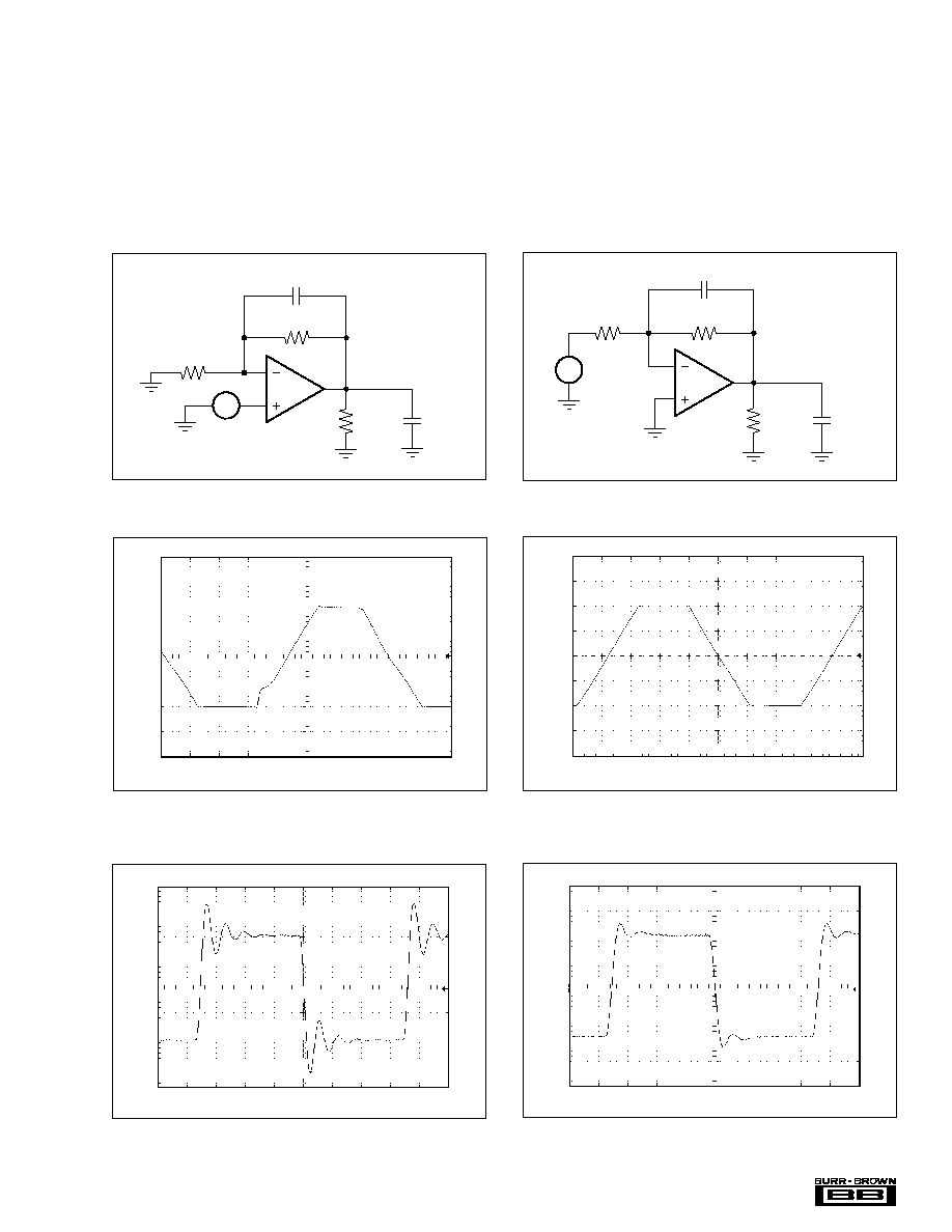
USING THE OPA228 IN LOW GAINS
The OPA228 family is intended for applications with signal
gains of 5 or greater, but it is possible to take advantage of
their high speed in lower gains. Without external compen-
sation, the OPA228 has sufficient phase margin to maintain
stability in unity gain with purely resistive loads. However,
the addition of load capacitance can reduce the phase
margin and destabilize the op amp.
A variety of compensation techniques have been evaluated
specifically for use with the OPA228. The recommended
configuration consists of an additional capacitor (C
F
) in
parallel with the feedback resistance, as shown in Figures
8 and 11. This feedback capacitor serves two purposes in
compensating the circuit. The op amp's input capacitance
and the feedback resistors interact to cause phase shift that
can result in instability. C
F
compensates the input capaci-
tance, minimizing peaking. Additionally, at high frequen-
cies, the closed-loop gain of the amplifier is strongly
influenced by the ratio of the input capacitance and the
feedback capacitor. Thus, C
F
can be selected to yield good
stability while maintaining high speed.
R
4
9.09k
R
3
1k
R
7
97.6k
R
6
40.2k
C
2
1
µ
F
C
1
1
µ
F
C
3
0.47
µ
F
C
4
22nF
R
2
2M
R
8
402k
R
5
634k
Input from
Device
Under
Test
R
1
2M
(OPA227)
U1
(OPA227)
U2
6
2
3
R
10
226k
R
9
178k
C
5
0.47
µ
F
C
6
10nF
R
11
178k
(OPA227)
U3
6
V
OUT
2
3
100k
V
OUT
6
2
3
OPA227
22pF
10
Device
Under
Test
15
Æ
OPA227, 2227, 4227
OPA228, 2228, 4228
Without external compensation, the noise specification of
the OPA228 is the same as that for the OPA227 in gains of
5 or greater. With the additional external compensation, the
output noise of the of the OPA228 will be higher. The
amount of noise increase is directly related to the increase
in high frequency closed-loop gain established by the C
IN
/
C
F
ratio.
Figures 8 and 11 show the recommended circuit for gains
of +2 and ≠2, respectively. The figures suggest approximate
FIGURE 8. Compensation of the OPA228 for G =+2.
FIGURE 9. Large-Signal Step Response, G = +2, C
LOAD
=
100pF, Input Signal = 5Vp-p.
FIGURE 10. Small-Signal Step Response, G = +2, C
LOAD
=
100pF, Input Signal = 50mVp-p.
400ns/div
25mV/div
values for C
F
. Because compensation is highly dependent
on circuit design, board layout, and load conditions, C
F
should be optimized experimentally for best results. Fig-
ures 9 and 10 show the large- and small-signal step re-
sponses for the G = +2 configuration with 100pF load
capacitance. Figures 12 and 13 show the large- and small-
signal step responses for the G = ≠2 configuration with
100pF load capacitance.
200ns/div
25mV/div
FIGURE 11. Compensation for OPA228 for G = ≠2.
FIGURE 12. Large-Signal Step Response, G = ≠2, C
LOAD
=
100pF, Input Signal = 5Vp-p.
400ns/div
25mV/div
200ns/div
25mV/div
FIGURE 13. Small-Signal Step Response, G = ≠2, C
LOAD
=
100pF, Input Signal = 50mVp-p.
2k
OPA228
22pF
2k
100pF
2k
1k
2k
15pF
OPA228
2k
100pF
OPA228
OPA228
OPA228
OPA228
16
Æ
OPA227, 2227, 4227
OPA228, 2228, 4228
FIGURE 15. Long-Wavelength Infrared Detector Amplifier.
FIGURE 16. High Performance Synchronous Demodulator.
V
OUT
V
IN
OPA227
68nF
10nF
33nF
330pF
2.2nF
OPA227
1.43k
1.91k
2.21k
1.43k
1.1k
1.65k
1.1k
f
N
= 13.86kHz
Q = 1.186
f
N
= 20.33kHz
f = 7.2kHz
Q = 4.519
dc Gain = 1
Output
NOTE: Use metal film resistors
and plastic film capacitor. Circuit
must be well shielded to achieve
low noise.
Responsivity
2.5 x 10
4
V/W
Output Noise
30
µ
Vrms, 0.1Hz to 10Hz
Dexter 1M
Thermopile
Detector
100
100k
OPA227
2
3
6
0.1
µ
F
Output
4.99k
D2
D1
DG188
TTL
In
S1
S2
9.76k
500
Balance
Trim
OPA227
2
3
1
8
6
20pF
10k
1k
4.75k
Offset
Trim
4.75k
+V
CC
Input
TTL INPUT
"1"
"0"
GAIN
+1
≠1
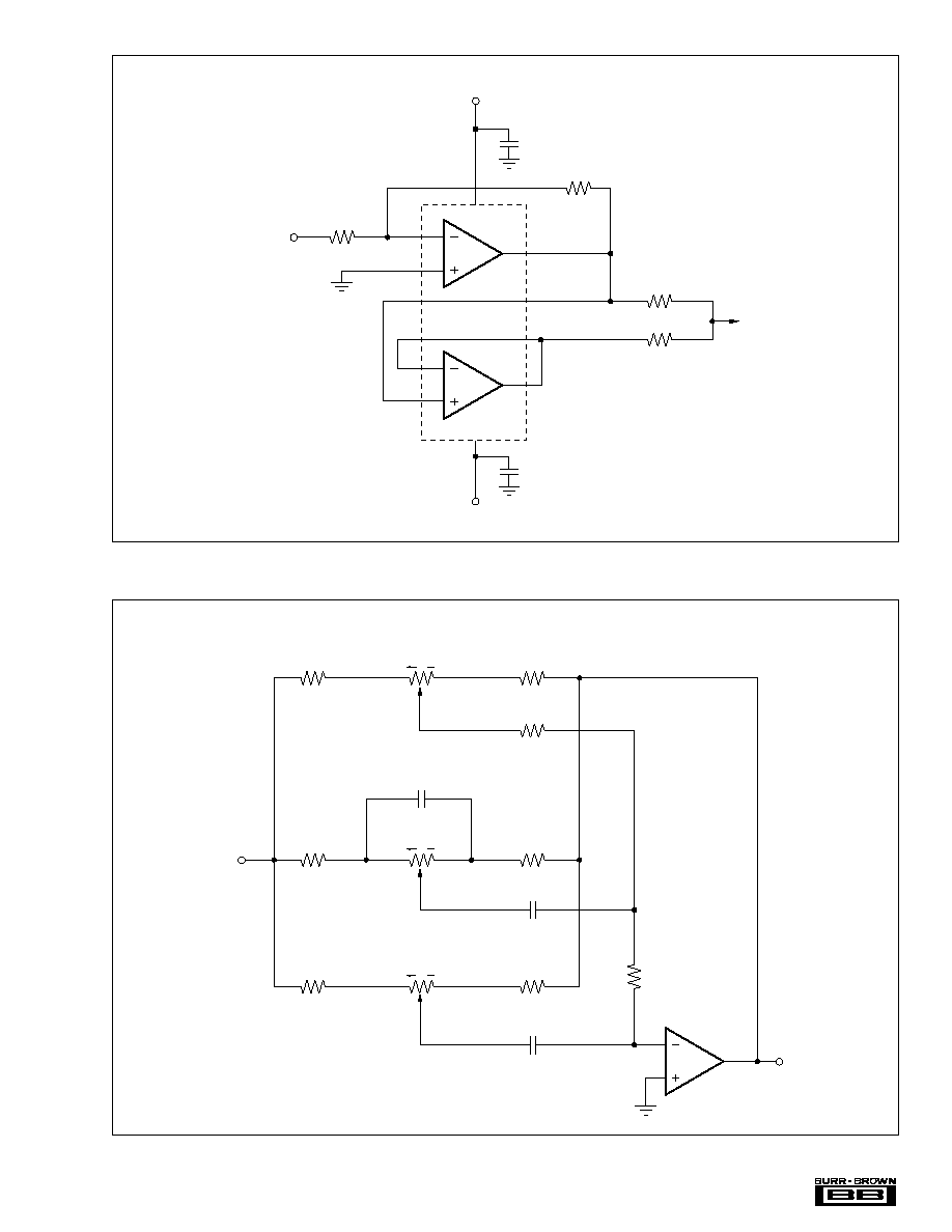
FIGURE 14. Three-Pole, 20kHz Low Pass, 0.5dB Chebyshev Filter.
17
Æ
OPA227, 2227, 4227
OPA228, 2228, 4228
FIGURE 17. Headphone Amplifier.
FIGURE 18. Three-Band ActiveTone Control (bass, midrange and treble).
200
200
1k
1k
1/2
OPA2227
1/2
OPA2227
≠15V
0.1
µ
F
0.1
µ
F
+15V
Audio
In
This application uses two op amps
in parallel for higher output current drive.
To
Headphone
R
5
50k
R
4
2.7k
V
IN
V
OUT
R
6
2.7k
C
1
940pF
C
2
0.0047
µ
F
C
3
680pF
CW
CW
R
2
50k
R
1
7.5k
R
3
7.5k
R
10
100k
R
8
50k
R
7
7.5k
R
9
7.5k
R
11
100k
CW
Bass Tone Control
Midrange Tone Control
Treble Tone Control
1
3
6
2
3
2
1
3
2
1
3
2
OPA227