 | –≠–ª–µ–∫—Ç—Ä–æ–Ω–Ω—ã–π –∫–æ–º–ø–æ–Ω–µ–Ω—Ç: OPA336NA | –°–∫–∞—á–∞—Ç—å:  PDF PDF  ZIP ZIP |

1
2
3
4
8
7
6
5
NC
V+
Output
NC
NC
≠In
+In
V≠
OPA336
8-Pin DIP, SO-8
1
2
3
5
4
V+
≠In
Out
V≠
+In
OPA336
SOT-23-5
1
2
3
4
8
7
6
5
V+
Out B
≠In B
+In B
Out A
≠In A
+In A
V≠
OPA2336
8-Pin DIP, SO-8, MSOP-8
A
B
FEATURES
q
SINGLE SUPPLY OPERATION
q
RAIL-TO-RAIL OUTPUT (within 3mV)
q
Micro
POWER: I
Q
= 20
µ
A/Amplifier
q
Micro
SIZE PACKAGES
q
LOW OFFSET VOLTAGE: 125
µ
V max
q
SPECIFIED FROM V
S
= 2.3V to 5.5V
q
SINGLE, DUAL, AND QUAD VERSIONS
(1)
OPA336
OPA2336
OPA4336
Æ
© 1997 Burr-Brown Corporation
PDS-1380C
Printed in U.S.A. August, 1997
SINGLE-SUPPLY,
Micro
POWER
CMOS OPERATIONAL AMPLIFIERS
Micro
Amplifier
TM
Series
APPLICATIONS
q
BATTERY POWERED INSTRUMENTS
q
PORTABLE DEVICES
q
HIGH IMPEDANCE APPLICATIONS
q
PHOTODIODE PRE-AMPS
q
PRECISION INTEGRATORS
q
MEDICAL INSTRUMENTS
q
TEST EQUIPMENT
DESCRIPTION
OPA336 series micropower CMOS operational ampli-
fiers are designed for battery powered applications.
They operate on a single supply with operation as low
as 2.1V. The output is rail-to-rail and swings to within
3mV of the supplies with a 100k
load. The common-
mode range extends to the negative supply--ideal for
single-supply applications. Single, dual, and quad
versions have identical specifications for maximum
design flexibility.
In addition to small size and low quiescent current
(20
µ
A/amplifier), they feature low offset voltage
(125
µ
V max), low input bias current (1pA), and high
open-loop gain (115dB). Dual and quad designs fea-
ture completely independent circuitry for lowest
crosstalk and freedom from interaction.
OPA336 packages are the tiny 5-lead SOT-23-5 surface
mount, SO-8 surface-mount, and 8-pin DIP. OPA2336
comes in the miniature MSOP-8 surface-mount, SO-8
surface-mount, and 8-pin DIP packages. OPA4336
packages are the space-saving SSOP-16 surface-mount
and the 14-pin DIP. All are specified from ≠40
∞
C to
+85
∞
C and operate from ≠55
∞
C to +125
∞
C. A
macromodel is available for design analysis.
OPA4336
OPA336
OPA2336
International Airport Industrial Park ∑ Mailing Address: PO Box 11400, Tucson, AZ 85734 ∑ Street Address: 6730 S. Tucson Blvd., Tucson, AZ 85706 ∑ Tel: (520) 746-1111 ∑ Twx: 910-952-1111
Internet: http://www.burr-brown.com/ ∑ FAXLine: (800) 548-6133 (US/Canada Only) ∑ Cable: BBRCORP ∑ Telex: 066-6491 ∑ FAX: (520) 889-1510 ∑ Immediate Product Info: (800) 548-6132
2
Æ
OPA336, 2336, 4336
The information provided herein is believed to be reliable; however, BURR-BROWN assumes no responsibility for inaccuracies or omissions. BURR-BROWN assumes
no responsibility for the use of this information, and all use of such information shall be entirely at the user's own risk. Prices and specifications are subject to change
without notice. No patent rights or licenses to any of the circuits described herein are implied or granted to any third party. BURR-BROWN does not authorize or warrant
any BURR-BROWN product for use in life support devices and/or systems.
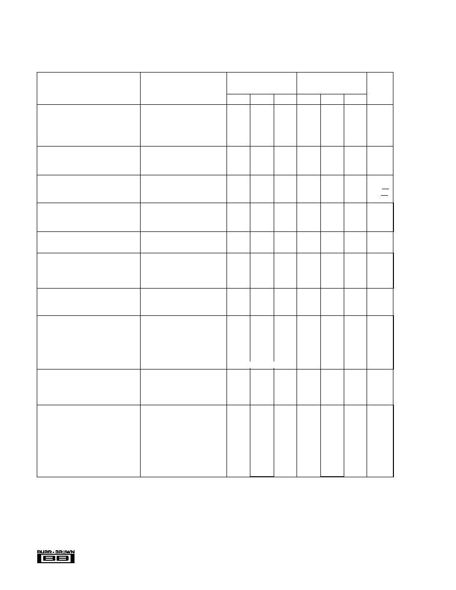
SPECIFICATIONS: V
S
= 2.3V to 5.5V
At T
A
= +25
∞
C, and R
L
= 25k
connected to V
S
/2, unless otherwise noted.
Boldface limits apply over the specified temperature range, ≠40
∞
C to +85
∞
C. V
S
= +5V.
OPA336NA, PA, UA
OPA336N, P, U
OPA2336EA, PA, UA
OPA2336E, P, U
OPA4336EA, PA
PARAMETER
CONDITION
MIN
TYP
(1)
MAX
MIN
TYP
(1)
MAX
UNITS
OFFSET VOLTAGE
Input Offset Voltage
V
OS
±
60
±
125
T
±
500
µ
V
vs Temperature
dV
OS
/dT
±
1.5
D
µ
V/
∞
C
vs Power Supply
PSRR
V
S
= 2.3V to 5.5V
25
100
T
T
µ
V/V
T
A
= ≠40
∞
C to +85
∞
C
V
S
= 2.3V to 5.5V
130
D
µ
V/V
Channel Separation, dc
0.1
T
µ
V/V
INPUT BIAS CURRENT
Input Bias Current
I
B
±
1
±
10
T
T
pA
T
A
= ≠40
∞
C to +85
∞
C
±
60
D
pA
Input Offset Current
I
OS
±
1
±
10
T
T
pA
NOISE
Input Voltage Noise, f = 0.1 to 10Hz
3
T
µ
Vp-p
Input Voltage Noise Density, f = 1kHz e
n
40
T
nV/
Hz
Current Noise Density, f = 1kHz
i
n
30
T
fA/
Hz
INPUT VOLTAGE RANGE
Common-Mode Voltage Range
V
CM
≠0.2
(V+) ≠1
T
T
V
Common-Mode Rejection Ratio
CMRR
≠0.2V < V
CM
< (V+) ≠1V
80
90
76
86
dB
T
A
= ≠40
∞
C to +85
∞
C
≠0.2V < V
CM
< (V+) ≠1V
76
74
dB
INPUT IMPEDANCE
Differential
10
13
|| 2
T
|| pF
Common-Mode
10
13
|| 4
T
|| pF
OPEN-LOOP GAIN
Open-Loop Voltage Gain
A
OL
R
L
= 25k
, 100mV < V
O
< (V+) ≠100mV
100
115
90
T
dB
T
A
= ≠40
∞
C to +85
∞
C
R
L
= 25k
, 100mV < V
O
< (V+) ≠100mV
100
90
dB
R
L
= 5k
, 500mV < V
O
< (V+) ≠500mV
90
106
T
T
dB
T
A
= ≠40
∞
C to +85
∞
C
R
L
= 5k
, 500mV < V
O
< (V+) ≠500mV
90
D
dB
FREQUENCY RESPONSE
Gain-Bandwidth Product
GBW
V
S
= 5V, G = 1
100
T
kHz
Slew Rate
SR
V
S
= 5V, G = 1
0.03
T
V/
µ
s
Overload Recovery Time
V
IN
∑ G = V
S
100
T
µ
s
OUTPUT
Voltage Output Swing from Rail
(2)
R
L
= 100k
, A
OL
70dB
3
T
mV
R
L
= 25k
,
A
OL
90dB
20
100
T
T
mV
T
A
= ≠40
∞
C to +85
∞
C
R
L
= 25k
,
A
OL
90dB
100
D
mV
R
L
= 5k
, A
OL
90dB
70
500
T
T
mV
T
A
= ≠40
∞
C to +85
∞
C
R
L
= 5k
, A
OL
90dB
500
D
mV
Short-Circuit Current
I
SC
±
5
T
mA
Capacitive Load Drive
C
LOAD
See Text
T
pF
POWER SUPPLY
Specified Voltage Range
V
S
2.3
5.5
T
T
V
Minimum Operating Voltage
2.1
T
V
Quiescent Current (per amplifier)
I
Q
I
O
= 0
20
32
T
T
µ
A
T
A
= ≠40
∞
C to +85
∞
C
I
O
= 0
36
D
µ
A
TEMPERATURE RANGE
Specified Range
≠40
+85
T
T
∞
C
Operating Range
≠55
+125
T
T
∞
C
Storage Range
≠55
+125
T
T
∞
C
Thermal Resistance
JA
SOT-23-5 Surface-Mount
200
T
∞
C/W
MSOP-8 Surface-Mount
150
T
∞
C/W
SO-8 Surface-Mount
150
T
∞
C/W
8-Pin DIP
100
T
∞
C/W
SSOP-16 Surface-Mount
100
T
∞
C/W
14-Pin DIP
80
T
∞
C/W
T
Specifications same as OPA2336E, P, U.
NOTES: (1) V
S
= +5V. (2) Output voltage swings are measured between the output and positive and negative power supply rails.
3
OPA336, 2336, 4336
Æ
1
2
3
4
5
6
7
8
16
15
14
13
12
11
10
9
Out D
≠In D
+In D
V≠
+In C
≠In C
Out C
NC
Out A
≠In A
+In A
V+
+In B
≠In B
Out B
NC
OPA4336
A
D
B
C
1
2
3
4
5
6
7
14
13
12
11
10
9
8
Out D
≠In D
+In D
V≠
+In C
≠In C
Out C
Out A
≠In A
+In A
V+
+In B
≠In B
Out B
OPA4336
A
D
B
C
PACKAGE
SPECIFIED
DRAWING
TEMPERATURE
PACKAGE
ORDERING
TRANSPORT
PRODUCT
PACKAGE
NUMBER
(1)
RANGE
MARKING
NUMBER
(2)
MEDIA
Single
OPA336NA
5-Lead SOT-23-5
331
≠40
∞
C to +85
∞
C
A36
(3)
OPA336NA-250
Tape and Reel
"
"
"
"
"
OPA336NA-3K
Tape and Reel
OPA336N
5-Lead SOT-23-5
331
≠40
∞
C to +85
∞
C
A36
(3)
OPA336N-250
Tape and Reel
"
"
"
"
"
OPA336N-3K
Tape and Reel
OPA336PA
8-Pin DIP
006
≠40
∞
C to +85
∞
C
OPA336PA
OPA336PA
Rails
OPA336P
8-Pin DIP
006
≠40
∞
C to +85
∞
C
OPA336P
OPA336P
Rails
OPA336UA
SO-8 Surface-Mount
182
≠40
∞
C to +85
∞
C
OPA336UA
OPA336UA
Rails
(4)
OPA336U
SO-8 Surface-Mount
182
≠40
∞
C to +85
∞
C
OPA336U
OPA336U
Rails
(4)
Dual
OPA2336PA
8-Pin DIP
006
≠40
∞
C to +85
∞
C
OPA2336PA
OPA2336PA
Rails
OPA2336P
8-Pin DIP
006
≠40
∞
C to +85
∞
C
OPA2336P
OPA2336P
Rails
OPA2336UA
SO-8 Surface-Mount
182
≠40
∞
C to +85
∞
C
OPA2336UA
OPA2336UA
Rails
(4)
OPA2336U
SO-8 Surface-Mount
182
≠40
∞
C to +85
∞
C
OPA2336U
OPA2336U
Rails
(4)
OPA2336EA
MSOP-8 Surface-Mount
337
≠40
∞
C to +85
∞
C
B36
(3)
OPA2336EA-250
Tape and Reel
"
"
"
"
"
OPA2336EA-2500
Tape and Reel
OPA2336E
MSOP-8 Surface-Mount
337
≠40
∞
C to +85
∞
C
B36
(3)
OPA2336E-250
Tape and Reel
"
"
"
"
"
OPA2336E-2500
Tape and Reel
Quad
OPA4336EA
SSOP-16 Surface-Mount
322
≠40
∞
C to +85
∞
C
OPA4336EA
OPA4336EA-250
Tape and Reel
"
"
"
"
"
OPA4336EA-2500
Tape and Reel
OPA4336PA
14-Pin DIP
010
≠40
∞
C to +85
∞
C
OPA4336PA
OPA4336PA
Rails
NOTES: (1) For detailed drawing and dimension table, please see end of data sheet, or Appendix C of Burr-Brown IC Data Book. (2) Models with -250, -2500, and
-3K are available only in Tape and Reel in the quantities indicated (e.g., -250 indicates 250 devices per reel). Ordering 3000 pieces of "OPA336NA-3K" will get
a single 3000 piece Tape and Reel. For detailed Tape and Reel mechanical information, refer to Appendix B of Burr-Brown IC Data Book. (3) Grade will be marked
on the Reel. (4) SO-8 models also available in Tape and Reel.
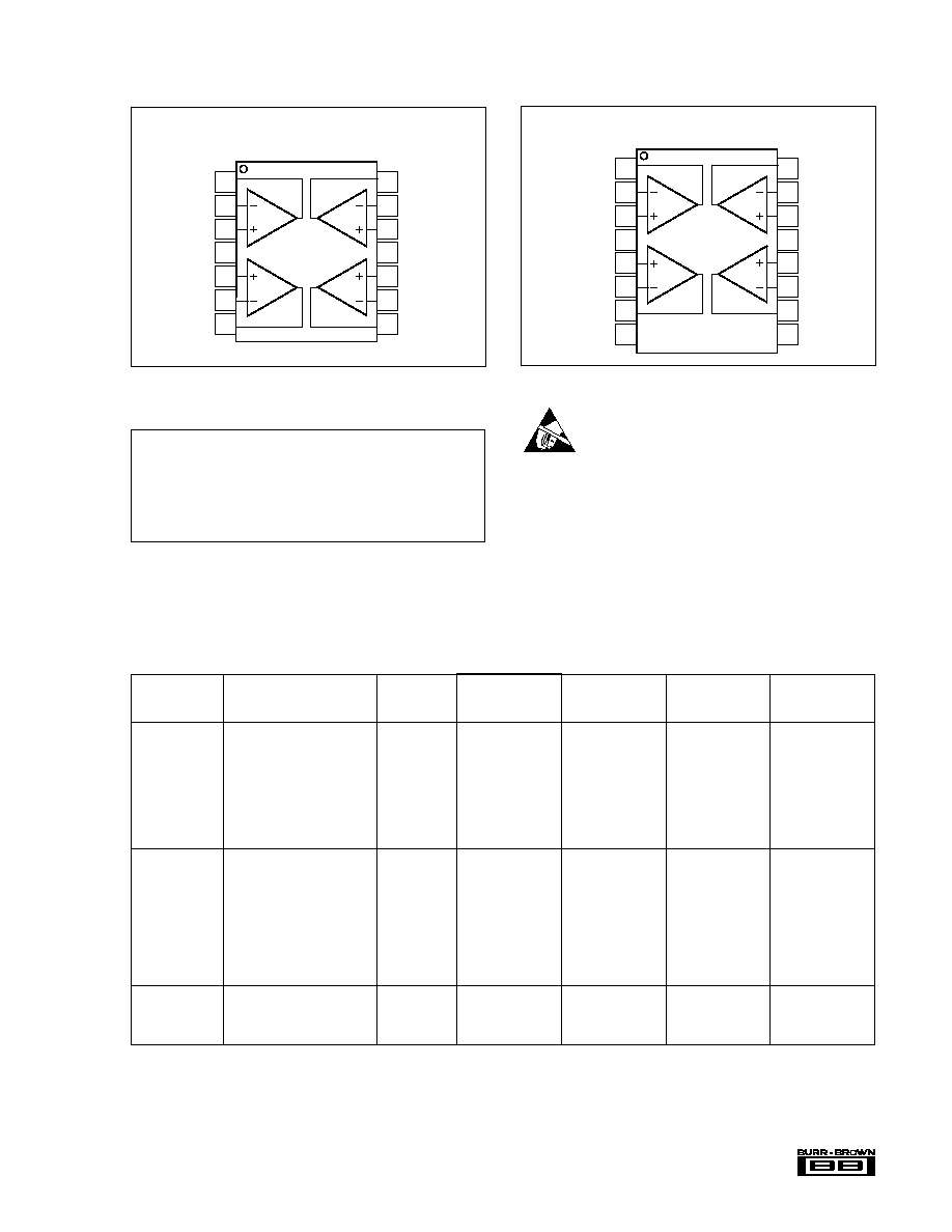
PACKAGE/ORDERING INFORMATION
ELECTROSTATIC
DISCHARGE SENSITIVITY
This integrated circuit can be damaged by ESD. Burr-Brown
recommends that all integrated circuits be handled with
appropriate precautions. Failure to observe proper handling
and installation procedures can cause damage.
ESD damage can range from subtle performance degrada-
tion to complete device failure. Precision integrated circuits
may be more susceptible to damage because very small
parametric changes could cause the device not to meet its
published specifications.
Supply Voltage ................................................................................... 5.5V
Signal Input Terminals, Voltage
(2)
.................... (V≠) ≠0.3V to (V+) +0.3V
Current
(2)
.................................................... 10mA
Output Short-Circuit
(3)
.............................................................. Continuous
Operating Temperature ................................................. ≠55
∞
C to +125
∞
C
Storage Temperature ..................................................... ≠55
∞
C to +125
∞
C
Junction Temperature ...................................................................... 150
∞
C
Lead Temperature (soldering, 10s) ................................................. 300
∞
C
NOTES: (1) Stresses above these ratings may cause permanent damage.
(2) Input terminals are diode-clamped to the power supply rails. Input signals
that can swing more than 0.3V beyond the supply rails should be current-
limited to 10mA or less. (3) Short-circuit to ground, one amplifier per
package.
ABSOLUTE MAXIMUM RATINGS
(1)
PIN CONFIGURATIONS
Top View
DIP
Top View
SSOP

4
Æ
OPA336, 2336, 4336
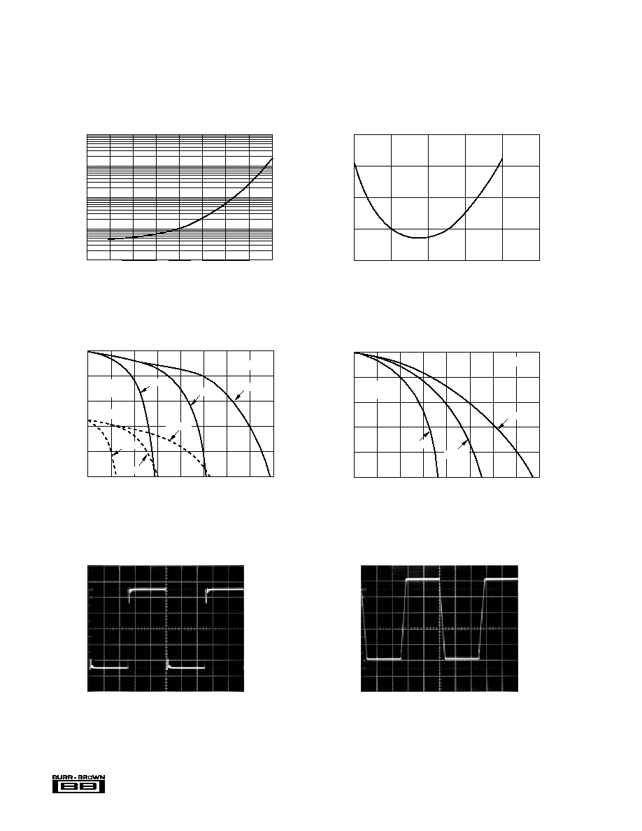
TYPICAL PERFORMANCE CURVES
At T
A
= +25
∞
C, V
S
= +5V, and R
L
= 25k
connected to V
S
/2, unless otherwise noted.
OPEN-LOOP GAIN/PHASE vs FREQUENCY
1
100
80
60
40
20
0
≠20
Voltage Gain (dB)
0
≠45
≠90
≠135
≠180
Phase (∞)
Frequency (Hz)
10
100
1k
10k
100k
1M
G
SHORT-CIRCUIT CURRENT vs SUPPLY VOLTAGE
Supply Voltage (V)
Short-Circuit Current (mA)
±6
±5
±4
±3
±2
±1
0
2.0
2.5
3.0
3.5
4.0
4.5
5.0
5.5
6.0
+I
SC
≠I
SC
POWER SUPPLY and COMMON-MODE
REJECTION RATIO vs FREQUENCY
100
80
60
40
20
0
PSRR, CMRR (dB)
Frequency (Hz)
1
10
100
1k
10k
100k
CMRR
PSRR
SHORT-CIRCUIT CURRENT vs TEMPERATURE
Temperature (∞C)
Short-Circuit Current (mA)
8
7
6
5
4
3
2
1
0
≠75
≠50
≠25
0
25
50
75
100
125
V
S
= +2.3V
V
S
= +5V
≠I
SC
+I
SC
+I
SC
≠I
SC
QUIESCENT CURRENT vs SUPPLY VOLTAGE
Supply Voltage (V)
Quiescent Current (
µ
A)
30
25
20
15
10
2.0
2.5
3.0
3.5
4.0
4.5
5.0
5.5
6.0
Per Amplifier
QUIESCENT CURRENT vs TEMPERATURE
Temperature (∞C)
Quiescent Current (
µ
A)
30
25
20
15
10
5
0
≠75
≠50
≠25
0
25
50
75
100
125
V
S
= +2.3V
V
S
= +5V
Per Amplifier

5
OPA336, 2336, 4336
Æ
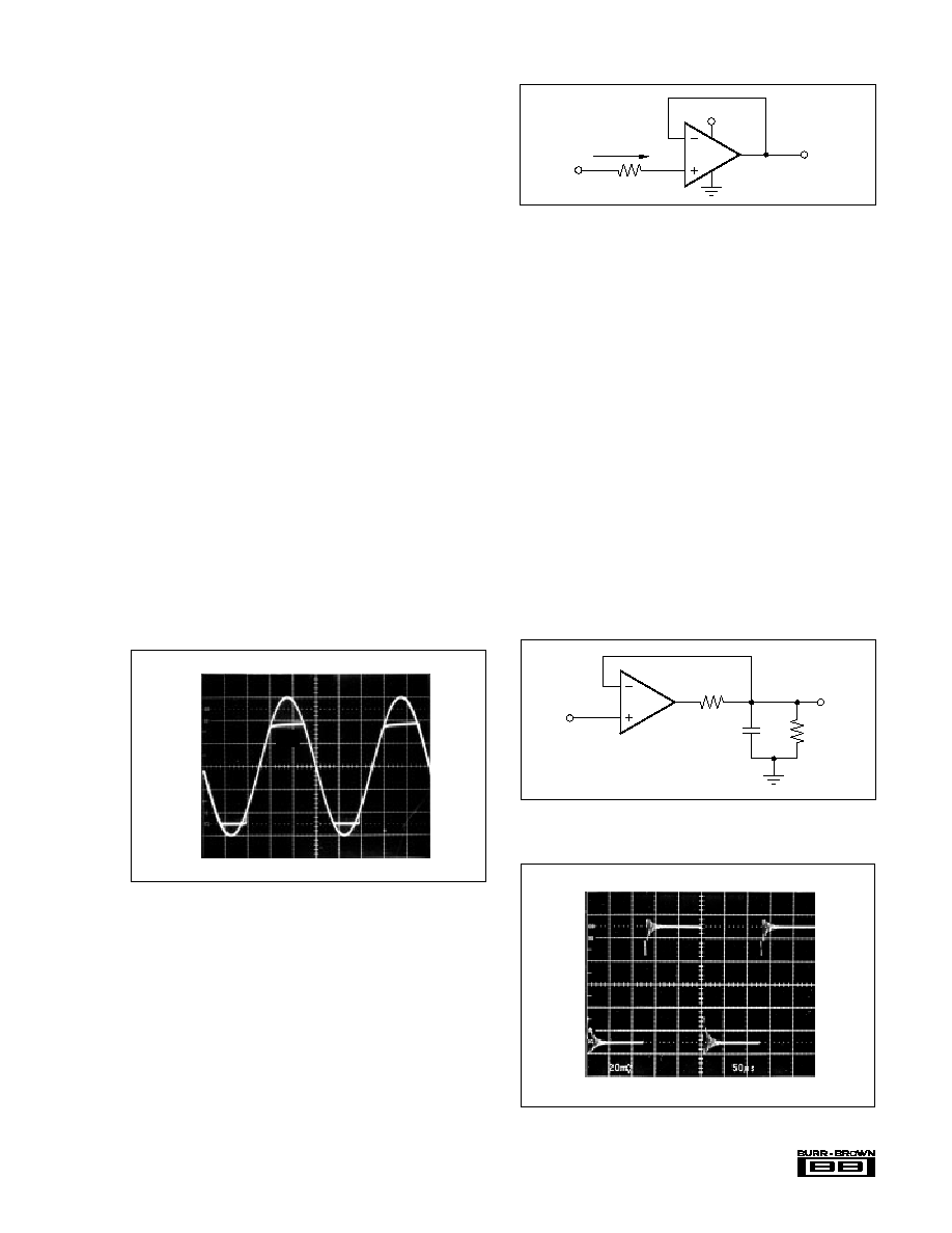
TYPICAL PERFORMANCE CURVES
(CONT)
At T
A
= +25
∞
C, V
S
= +5V, and R
L
= 25k
connected to V
S
/2, unless otherwise noted.
MAXIMUM OUTPUT VOLTAGE vs FREQUENCY
100k
10k
Frequency (Hz)
100
1k
6
5
4
3
2
1
0
Output Voltage (Vp-p)
V
S
= +5.5V
V
S
= +2.3V
OFFSET VOLTAGE
PRODUCTION DISTRIBUTION
Percent of Amplifiers (%)
Offset Voltage (µV)
≠500
≠400
≠300
≠200
≠100
0
100
200
300
400
500
25
20
15
10
5
0
0.1%
0.2%
0.3%
0.1%
Typical production
distribution of
packaged units.
A
OL
, CMRR, PSRR vs TEMPERATURE
Temperature (∞C)
A
OL
, CMRR, PSRR (dB)
120
110
100
90
80
70
≠75
≠50
≠25
0
25
50
75
100
125
A
OL
PSRR
CMRR
OFFSET VOLTAGE DRIFT MAGNITUDE
PRODUCTION DISTRIBUTION
Percent of Amplifiers (%)
Offset Voltage Drift (µV/∞C)
0.25
0.5
0.75
1
1.25
1.5
1.75
2
2.25
2.5
2.75
3
3.25
3.5
3.75
4
25
20
15
10
5
0
Typical production
distribution of
packaged units.
INPUT VOLTAGE AND CURRENT NOISE
SPECTRAL DENSITY vs FREQUENCY
Frequency (Hz)
1k
100
10
1
1k
100
10
1
10
100
1k
10k
100k
Voltage Noise (nV/
Hz)
Current Noise (fA/
Hz)
Voltage Noise
Current Noise
CHANNEL SEPARATION vs FREQUENCY
Frequency (Hz)
Channel Separation (dB)
150
140
130
120
110
100
1k
10k
100k
Dual and Quad devices, G = 1, all
channels. Quad measured channel A
to D or B to C--other combinations
yield improved rejection.
6
Æ
OPA336, 2336, 4336
TYPICAL PERFORMANCE CURVES
(CONT)
At T
A
= +25
∞
C, V
S
= +5V, and R
L
= 25k
connected to V
S
/2, unless otherwise noted.
SMALL-SIGNAL STEP RESPONSE
G = 1, C
L
= 200pF, V
S
= +5V
50
µ
s/div
LARGE-SIGNAL STEP RESPONSE
G = 1, C
L
= 620pF, V
S
= +5V
20mV/div
200
µ
s/div
INPUT BIAS CURRENT vs TEMPERATURE
Input Bias Current (pA)
Temperature (∞C)
≠75
≠50
≠25
0
25
50
75
100
125
1k
100
10
1
0.1
OUTPUT VOLTAGE SWING vs OUTPUT CURRENT
Output Voltage (V)
Output Current (mA)
≠0
≠1
≠2
≠3
≠4
≠5
≠6
≠7
≠8
≠2.5
≠2.0
≠1.5
≠1.0
≠0.5
0
Sinking
Current
+25∞C
≠55∞C
+125∞C
V
S
= ±2.5V
INPUT BIAS CURRENT
vs INPUT COMMON-MODE VOLTAGE
Input Bias Current (pA)
Common-Mode Voltage (V)
0
1
2
3
4
5
4
3
2
1
0
V
S
= +5V
500mV/div
OUTPUT VOLTAGE SWING vs OUTPUT CURRENT
Output Voltage (V)
Output Current (mA)
0
1
2
3
4
5
6
7
8
5
4
3
2
1
0
Sourcing
Current
≠55∞C
+25∞C
+125∞C
+125∞C
+25∞C
≠55∞C
V
S
= +2.3V
V
S
= +5V
7
OPA336, 2336, 4336
Æ
FIGURE 4. Small-Signal Step Response Using Series Re-
sistor to Improve Capacitive Load Drive.
R
S
= 100
, Load = 25k
|| 1000pF, V
S
= +5V
50
µ
s/div
20mV/div
FIGURE 2. Input Current Protection for Voltages Exceeding
the Supply Voltage.
CAPACITIVE LOAD AND STABILITY
OPA336 series op amps can drive a wide range of capaci-
tive loads. However, all op amps under certain conditions
may become unstable. Op amp configuration, gain, and
load value are just a few of the factors to consider when
determining stability.
When properly configured, OPA336 series op amps can
drive approximately 10,000pF. An op amp in unity gain
configuration is the most vulnerable to capacitive load. The
capacitive load reacts with the op amp's output resistance,
along with any additional load resistance, to create a pole in
the response which degrades the phase margin. In unity gain,
OPA336 series op amps perform well with a pure capacitive
load up to about 300pF. Increasing gain enhances the
amplifier's ability to drive loads beyond this level.
One method of improving capacitive load drive in the unity
gain configuration is to insert a 50
to 100
resistor inside
the feedback loop as shown in Figure 3. This reduces ringing
with large capacitive loads while maintaining DC accuracy.
R
S
100
OPAx336
C
L
R
L
V
IN
V
OUT
FIGURE 3. Series Resistor in Unity-Gain Configuration
Improves Capacitive Load Drive.
FIGURE 1. No Phase Inversion with Inputs Greater than the
Power Supply Voltage.
APPLICATIONS INFORMATION
OPA336 series op amps are fabricated on a state-of-the-art
0.6 micron CMOS process. They are unity-gain stable and
suitable for a wide range of general purpose applications.
Power supply pins should be bypassed with 0.01
µ
F ceramic
capacitors. OPA336 series op amps are protected against
reverse battery voltages.
OPERATING VOLTAGE
OPA336 series op amps can operate from a +2.1V to +5.5V
single supply with excellent performance. Most behavior
remains unchanged throughout the full operating voltage
range. Parameters which vary significantly with operating
voltage are shown in the typical performance curves. OPA336
series op amps are fully specified for operation from +2.3V
to +5.5V; a single limit applies over the supply range. In
addition, many parameters are guaranteed over the specified
temperature range, ≠40
∞
C to +85
∞
C.
INPUT VOLTAGE
The input common-mode range of OPA336 series op amps
extends from (V≠) ≠0.2V to (V+) ≠1V. For normal opera-
tion, inputs should be limited to this range. The absolute
maximum input voltage is 300mV beyond the supplies.
Thus, inputs greater than the input common-mode range
but less than maximum input voltage, while not valid, will
not cause any damage to the op amp. Furthermore, the
inputs may go beyond the power supplies without phase
inversion (Figure 1) unlike some other op amps.
6V
0V
V
OUT
Normally, input bias current is approximately 1pA. How-
ever, input voltages exceeding the power supplies can
cause excessive current to flow in or out of the input pins.
Momentary voltages greater than the power supply can be
tolerated as long as the current on the input pins is limited
to 10mA. This is easily accomplished with an input resis-
tor as shown in Figure 2.
5k
OPAx336
10mA max
+5V
V
IN
V
OUT
I
OVERLOAD

8
Æ
OPA336, 2336, 4336
For example, with R
L
= 25k
, OPA336 series op amps
perform well with capacitive loads in excess of 1000pF
(Figure 4). Without R
S
, capacitive load drive is typically
350pF for these conditions (see Figure 5).
Alternatively, the resistor may be connected in series with
the output outside of the feedback loop. However, if there is
a resistive load parallel to the capacitive load, it and the
series resistor create a voltage divider. This introduces a DC
error at the output. However, this error may be insignificant.
For instance, with R
L
= 100k
and R
S
= 100
, there is only
about a 0.1% error at the output.
Figure 5 shows the recommended operating regions for the
OPA336. Decreasing the load resistance generally improves
capacitive load drive. Figure 5 also illustrates how stability
differs depending on where the resistive load is connected.
With G = +1 and R
L
= 10k
connected to V
S
/2, the OPA336
can typically drive 500pF. Connecting the same load to
ground improves capacitive load drive to 1000pF.
FIGURE 5. Stability--Capacitive Load vs Resistive Load.
V
S
= +5V, V
O
= V
S
/2
Capacitive Load (pF)
Resistive Load (k
)
10
5
100
10k
1k
100
Operation Above Selected Gain
Curve Not Recommended
G = +1
R
L
to Ground
G = +2
R
L
to Ground
G = +1
R
L
to V
S
/2