 | –≠–ª–µ–∫—Ç—Ä–æ–Ω–Ω—ã–π –∫–æ–º–ø–æ–Ω–µ–Ω—Ç: OPA512 | –°–∫–∞—á–∞—Ç—å:  PDF PDF  ZIP ZIP |

OPA512
Very-High Current--High Power
OPERATIONAL AMPLIFIER
APPLICATIONS
q
SERVO AMPLIFIER
q
MOTOR DRIVER
q
SYNCRO EXCITATION
q
AUDIO AMPLIFIER
q
TEST PIN DRIVER
FEATURES
q
WIDE SUPPLY RANGE:
±
10V to
±
50V
q
HIGH OUTPUT CURRENT: 15A Peak
q
CLASS A/B OUTPUT STAGE:
Low Distortion
q
VOLTAGE-CURRENT LIMIT PROTECTION
CIRCUIT
q
SMALL TO-3 PACKAGE
DESCRIPTION
The OPA512 is a high voltage, very-high current
operational amplifier designed to drive a wide variety
of resistive and reactive loads. Its complementary
class A/B output stage provides superior performance
in applications requiring freedom from cross-over
distortion. User-set current limit circuitry provides
protection to the amplifier and load in fault conditions.
A resistor-programmable voltage-current limiter
circuit may be used to further protect the amplifier
from damaging conditions.
The OPA512 employs a laser-trimmed monolithic
integrated circuit to bias the output transistors, provid-
ing excellent low-level signal fidelity and high output
voltage swing. The reduced internal parts count made
possible with this monolithic IC improves perfor-
mance and reliability.
This hybrid integrated circuit is housed in a hermetic
TO-3 package and all circuitry is electrically-isolated
from the case. This allows direct mounting to a chassis
or heat sink without cumbersome insulating hardware
and provides optimum heat transfer.
Out
R
CL+
R
CL≠
8
7
2
Bias
Circuit
4
6
≠V
S
3
+V
S
5
1
R
VI
(Optional)
Æ
International Airport Industrial Park ∑ Mailing Address: PO Box 11400 ∑ Tucson, AZ 85734 ∑ Street Address: 6730 S. Tucson Blvd. ∑ Tucson, AZ 85706
Tel: (520) 746-1111 ∑ Twx: 910-952-1111 ∑ Cable: BBRCORP ∑ Telex: 066-6491 ∑ FAX: (520) 889-1510 ∑ Immediate Product Info: (800) 548-6132
©
1985 Burr-Brown Corporation
PDS-600B
Printed in U.S.A. December, 1993

Æ
OPA512
2
OPA512BM
OPA512SM
PARAMETER
CONDITIONS
MIN
TYP
MAX
MIN
TYP
MAX
UNITS
INPUT OFFSET VOLTAGE
Initial Offset
±
2
±
6
±
1
±
3
mV
vs Temperature
Specified Temp. Range
±
10
±
65
*
±
40
µ
V/
∞
C
vs Supply Voltage
±
30
±
200
*
*
µ
V/V
vs Power
±
20
*
µ
V/V
INPUT BIAS CURRENT
Initial
12
30
10
20
nA
vs Temperature
Specified Temp. Range
±
50
400
*
*
pA/
∞
C
vs Supply Voltage
±
10
*
pA/V
INPUT OFFSET CURRENT
Initial
±
12
±
30
±
5
±
10
nA
vs Temperature
Specfied Temp. Range
±
50
*
pA/
∞
C
INPUT IMPEDANCE, DC
200
*
M
INPUT CAPACITANCE
3
*
pF
VOLTAGE RANGE
Common-Mode Voltage
Specified Temp. Range
±
(|V
S
| ≠ 5)
±
(|V
S
| ≠ 3)
*
*
V
Common-Mode Rejection
Specified Temp. Range
74
100
*
*
dB
GAIN
Open-Loop Gain at 10Hz
1k
Load
110
*
dB
Specified Temp. Range
8
Load
96
108
*
*
dB
Gain-Bandwidth Product, 1MHz
8
Load
4
*
MHz
Power Bandwidth
8
Load
13
20
*
*
kHz
Phase Margin
Specified Temp. Range
8
Load
20
*
Degrees
OUTPUT
Voltage Swing
(1)
BM at 10A, SM at 15A
±
(|V
S
| ≠ 6)
±
(|V
S
| ≠ 7)
V
Specified Temp. Range
I
O
= 80mA
±
(|V
S
| ≠ 5)
*
V
I
O
= 5A
±
(|V
S
| ≠ 5)
*
V
Current, Peak
10
15
A
Settling Time to 0.1%
2V Step
2
*
µ
s
Slew Rate
2.5
4
*
*
V/
µ
s
Capacitive Load
Specified Temp. Range
G = 1
1.5
*
nF
Specified Temp. Range
G > 10
SOA
(2)
*
POWER SUPPLY
Voltage
Specified Temp. Range
±
10
±
40
±
45
*
*
±
50
V
Current, Quiescent
25
50
*
35
mA
THERMAL RESISTANCE
AC Junction-to-Case
(3)
T
C
= ≠55
∞
C to +125
∞
C,
f > 60Hz
0.8
0.9
*
*
∞
C/W
DC Junction-to-Case
T
C
= ≠55
∞
C to +125
∞
C
1.25
1.4
*
*
∞
C/W
Junction to Air
T
C
= ≠55
∞
C to +125
∞
C
30
*
∞
C/W
TEMPERATURE RANGE
Specified
T
C
≠25
+85
≠55
+125
∞
C
SPECIFICATIONS
ELECTRICAL
At T
C
= +25
∞
C, and V
S
=
±
40V, unless otherwise noted.
The information provided herein is believed to be reliable; however, BURR-BROWN assumes no responsibility for inaccuracies or omissions. BURR-BROWN assumes
no responsibility for the use of this information, and all use of such information shall be entirely at the user's own risk. Prices and specifications are subject to change
without notice. No patent rights or licenses to any of the circuits described herein are implied or granted to any third party. BURR-BROWN does not authorize or warrant
any BURR-BROWN product for use in life support devices and/or systems.
*Specification same as OPA512BM.
NOTES: (1) +V
S
and ≠V
S
denote the postive and negative supply voltage, respectively. Total V
S
is measured from +V
S
to ≠V
S
. (2) SOA = Safe Operating Area.
(3) Rating applies if the output current alternates between both output transistors at a rate faster than 60Hz.
Æ
OPA512
3
ORDERING INFORMATION
MODEL
PACKAGE
TEMPERATURE RANGE
OPA512BM
8-pin TO-3
≠25
∞
C to +85
∞
C
OPA512SM
8-pin TO-3
≠55
∞
C to +125
∞
C
ABSOLUTE MAXIMUM RATINGS
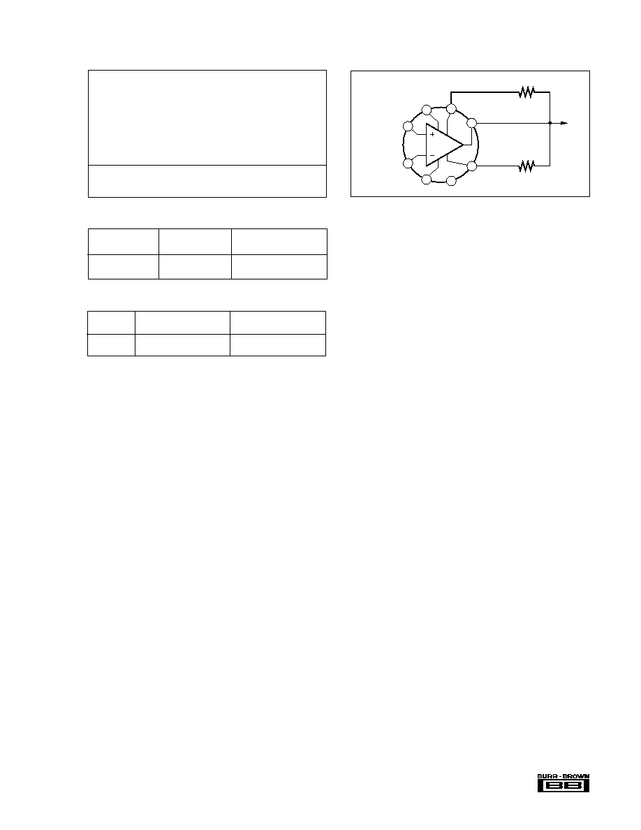
CONNECTION DIAGRAM
Supply Voltage, +V
S
to ≠V
S
................................................................ 100V
Output Current: Source ........................................................................ 15A
Sink .................................................................... see SOA
Power Dissipation, Internal
(1)
............................................................ 125W
Input Voltage: Differential ........................................................
±
(|V
S
| ≠ 3V)
Common-mode .............................................................
±
V
S
Temperature: Pins (soldering, 10s) ................................................ +300
∞
C
Junction
(1)
............................................................... +200
∞
C
Temperature Range: Storage
(2)
...................................... ≠65
∞
C to +150
∞
C
Operating (Case) .......................... ≠55
∞
C to +125
∞
C
NOTES: (1) Long term operation at the maximum junction temperature will
result in reduced product life. Derate internal power dissipation to achieve
high MTTF. (2) OPA512BM, ≠55
∞
C to +100
∞
C.
PACKAGE INFORMATION
PACKAGE DRAWING
MODEL
PACKAGE
NUMBER
(1)
OPA512BM
8-Pin TO-3
030
OPA512SM
8-Pin TO-3
030
NOTE: (1) For detailed drawing and dimension table, please see end of data
sheet, or Appendix D of Burr-Brown IC Data Book.
Top View
+V
S
2
3
4
1
8
7
5
6
≠Current
Limit
Output
+In
≠In
+Current
Limit
≠R
CL
≠V
S
R
VI
+R
CL

Æ
OPA512
4
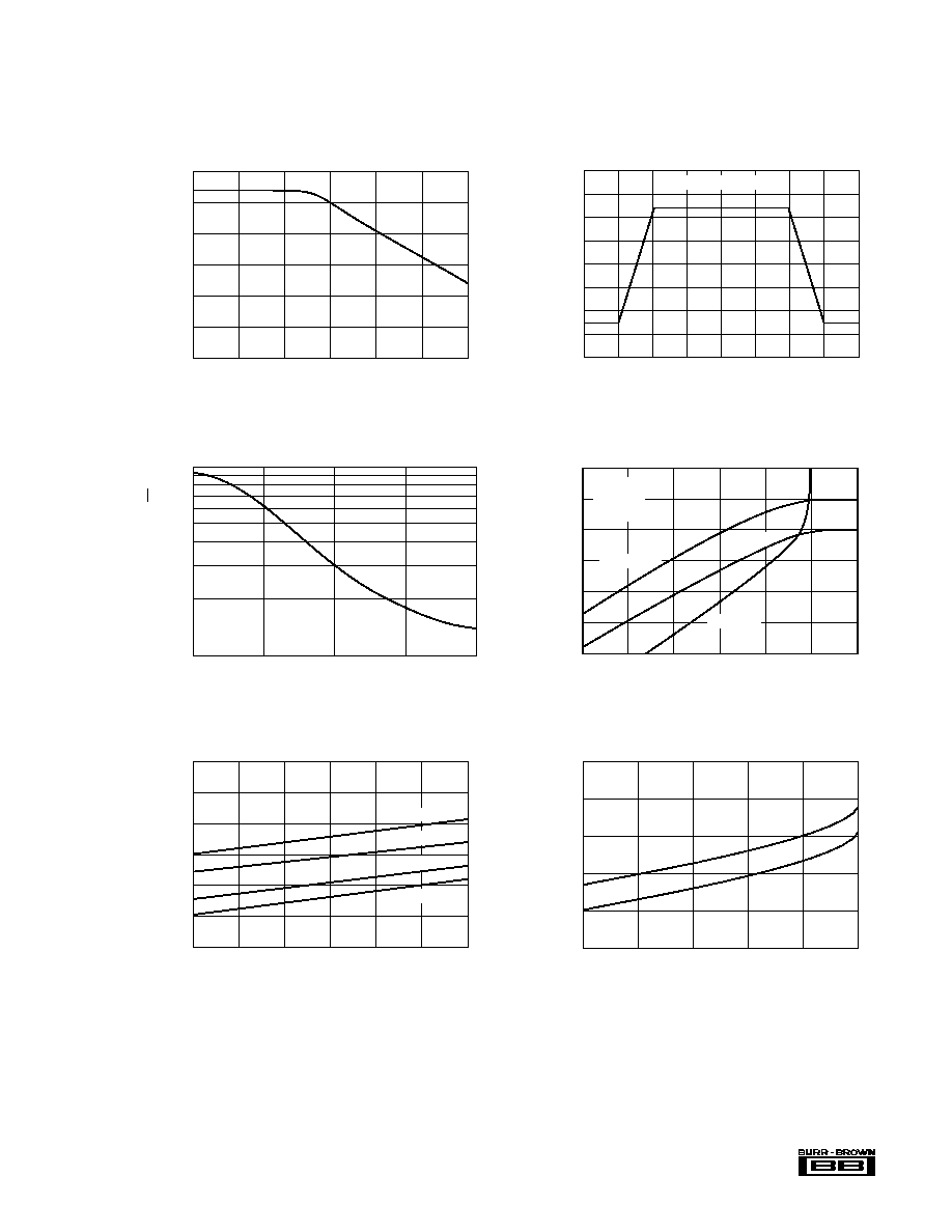
10
100
4.6
100
68
46
32
22
15
10
6.8
Output Voltage, V
O
(Vp-p)
Frequency, f (kHz)
POWER RESPONSE
|+V
S
| + |≠V
S
| = 100V
|+V
S
| + |≠V
S
| = 80V
|+V
S
| + |≠V
S
| = 30V
20
30
50
70
1
1k
10
100
10k
100k
1M
10M
≠210
0
≠30
≠60
≠90
≠120
≠150
≠180
Phase,
(degrees)
Frequency, f (Hz)
PHASE RESPONSE
1
1k
10
100
10k
100k
1M
10M
≠20
120
100
80
60
40
20
0
Open-Loop Gain, A (dB)
Frequency, f (Hz)
SMALL SIGNAL RESPONSE
≠50
25
≠25
0
50
75
100
125
0
17.5
15.0
12.5
10.0
7.5
5.0
2.5
Current Limit, I
LIM
(A)
CURRENT LIMIT
Case Temperature, T
C
(∞C)
R
CL
= 0.18
, R
VI
= 0
V
O
= 24V
V
O
= 0
V
O
= ≠24V
V
O
= 0
R
CL
= 0.06
, R
VI
=
≠50
25
≠25
0
50
75
100
125
0.4
2.5
2.2
1.9
1.6
1.3
1.0
0.7
Normalized Bias Current, I
B
BIAS CURRENT
Case Temperature, T
C
(∞C)
0
60
20
40
80
100
120
140
0
140
120
100
80
60
40
20
Internal Power Dissipation, P (W)
Case Temperature, T
C
(∞C)
POWER DERATING
SM
BM
TYPICAL PERFORMANCE CURVES
T
A
= 25
∞
C, V
S
=
±
40VDC, unless otherwise noted.
Æ
OPA512
5
0
15
1
6
5
4
3
2
Voltage Drop From Supply (V)
Output Current, I
O
(A)
OUTPUT VOLTAGE SWING
3
6
9
12
≠V
O
+V
O
40
100
0.4
1.6
1.4
1.2
1.0
0.8
0.6
Normalized, I
Q
Total Supply Voltage, V
S
(V)
QUIESCENT CURRENT
50
60
70
80
90
T
C
= +25∞C
T
C
= +85∞C
T
C
= +125∞C
T
C
= ≠25∞C
100
100k
0.003
3
1
0.3
0.1
0.03
0.01
Distortion (%)
Frequency, f (Hz)
HARMONIC DISTORTION
300
1k
3k
10k
30k
G = 10
V
S
= ±37V
R
L
= 4
P
O
= 100mW
P
O
= 120W
P
O
= 4W
0
100k
10
Input Noise Voltage, V
N
(nV/
Hz)
Frequency, f (Hz)
INPUT NOISE
100
1k
10k
20
30
40
50
70
100
0
12
≠8
8
6
4
2
0
≠2
≠4
≠6
Output Voltage, V
O
(V)
Time, t (µs)
PULSE RESPONSE
2
4
6
8
10
V
IN
= ±5V, t
R
= 100ns
1
1M
0
120
100
80
60
40
20
Common-Mode Rejection, CMR (dB)
Frequency, f (Hz)
COMMON-MODE REJECTION
10
100
1k
10k
100k
TYPICAL PERFORMANCE CURVES
(CONT)
T
A
= 25
∞
C, V
S
=
±
40VDC, unless otherwise noted.