 | ÐлекÑÑоннÑй компоненÑ: OPA600CM | СкаÑаÑÑ:  PDF PDF  ZIP ZIP |
Äîêóìåíòàöèÿ è îïèñàíèÿ www.docs.chipfind.ru
©
1986 Burr-Brown Corporation
PDS-672
Printed in U.S.A. March, 1992
Fast-Settling Wideband
OPERATIONAL AMPLIFIER
FEATURES
APPLICATIONS
q
FAST SETTLING: 80ns to
±
0.1%
100ns to
±
0.01%
q
FULL DIFFERENTIAL FET INPUT
q
25
°
C to +85
°
C AND
55
°
C to +125
°
C TEMPERATURE
RANGES
q
±
10V OUTPUT: 200mA
q
GAIN BANDWIDTH PRODUCT: 5GHz
q
VOLTAGE CONTROLLED OSCILLATOR
DRIVER
q
LARGE SIGNAL, WIDEBAND DRIVERS
q
HIGH SPEED D/A CONVERTER OUTPUT
AMPLIFIER
q
VIDEO PULSE AMPLIFIER
DESCRIPTION
the settling time for various gains and load conditions.
The OPA600 is useful in a broad range of video, high
speed test circuits and ECM applications. It is particu-
larly well suited to operate as a voltage controlled oscil-
lator (VCO) driver. It makes an excellent digital-to-ana-
log converter output amplifier. It is a workhorse in test
equipment where fast pulses, large signals,
and 50
drive are important. It is a good choice for
sample/holds, integrators, fast waveform generators, and
multiplexers.
The OPA600 is specified over the industrial temperature
range (OPA600BM, CM) and military temperature range
(OPA600SM, TM). The OPA600 is housed in a welded,
hermetic metal package.
The OPA600 is a wideband operational amplifier specifi-
cally designed for fast settling to
±
0.01% accuracy. It is
stable, easy to use, has good phase margin with minimum
overshoot, and it has excellent DC performance. It uti-
lizes an FET input stage to give low input bias current.
Its DC stability over temperature is outstanding. The slew
rate exceeds 400V/
µ
s. All of this combines to form an
outstanding amplifier for large and small signals.
High accuracy with fast settling time is achieved by using
a high open-loop gain which provides the accuracy at
high frequencies. The thermally balanced design main-
tains this accuracy without droop or thermal tail. Exter-
nal frequency compensation allows the user to optimize
OPA600
International Airport Industrial Park · Mailing Address: PO Box 11400 · Tucson, AZ 85734 · Street Address: 6730 S. Tucson Blvd. · Tucson, AZ 85706
Tel: (602) 746-1111 · Twx: 910-952-1111 · Cable: BBRCORP · Telex: 066-6491 · FAX: (602) 889-1510 · Immediate Product Info: (800) 548-6132
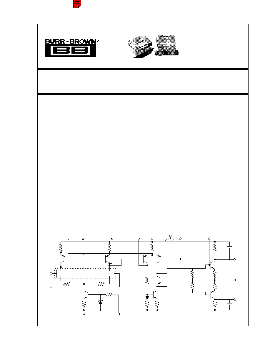
7
14
16
3
Fequency
Compensation
50
Current
Boost
50
8
9
11
12
5
4
15
2
100k
100k
100k
1
6
Output
Current
Boost
Common
+V
CC
Frequency
Compensation
Frequency
Compensation
Offset
Offset
+Input
Input
V
CC
Common
(Case)
13
Fequency
Compensation
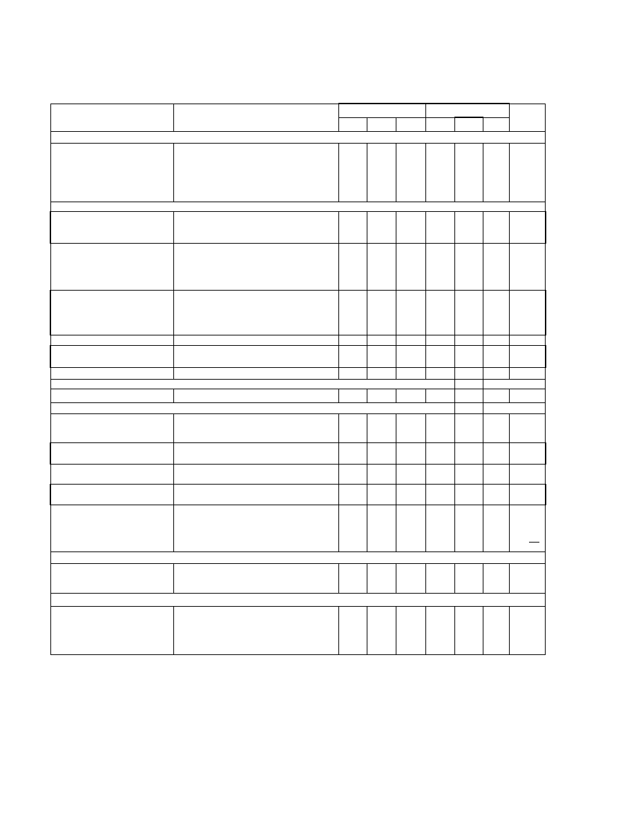
SPECIFICATIONS
ELECTRICAL
At V
CC
=
±
15VDC and T
A
= +25
°
C unless otherwise noted.
OPA600CM,TM
(1)
OPA600BM,SM
PARAMETER
CONDITIONS
MIN
TYP
MAX
MIN
TYP
MAX
UNITS
OUTPUT
Voltage
R
L
= 2k
±
10
*
V
R
L
= 50
(2)
±
9
*
V
Current
R
L
= 50
(2)
±
180
±
200
*
*
mA
Current Pulse
R
L
= 50
(3)
±
180
±
200
*
*
mA
Resistance
Open Loop DC
75
*
Short-Circuit Current
To COMMON Only, t
MAX
= 1s
(4)
250
300
*
*
mA
DYNAMIC RESPONSE
Settling Time
(5)
: to
±
0.01% (
±
1mV)
V
OUT
= 10V
100
125
*
*
ns
to
±
0.1% (
±
10mV)
V
OUT
= 10V
80
105
*
*
ns
to
±
1% (
±
100mV)
V
OUT
= 10V
70
95
*
*
ns
Gain-Bandwidth Product (open-loop)
C
C
= 0pF, G = 1V/V
150
*
MHz
C
C
= 0pF, G = 10V/V
500
*
MHz
C
C
= 0pF, G = 100V/V
1.5
*
GHz
C
C
= 0pF, G = 1000V/V
5
*
GHz
C
C
= 0pF, G = 10,000V/V
10
*
GHz
Bandwidth (3dB small signal)
(6)
G = +1V/V
125
*
MHz
G = 1V/V
90
*
MHz
G = 10V/V
95
*
MHz
G = 100V/V
20
*
MHz
G = 1000V/V
6
*
MHz
Full Power Bandwidth
V
OUT
=
±
5V, G = 1V/V, C
C
= 3.3pF, R
L
= 100
16
*
MHz
Slew Rate
V
OUT
=
±
5V, G = 1000V/V, C
C
= 0pF, R
L
= 100
500
*
V/
µ
s
V
OUT
=
±
5V,G = 1V/V
(4)
400
440
*
*
V/
µ
s
Phase Margin
G = 1V/V, C
C
= 3.3pF
40
*
Degrees
GAIN
Open-Loop Voltage Gain
f = DC, R
L
= 2k
, T
A
= +25
°
C
86
94
*
*
dB
INPUT
Offset Voltage
(7)
T
A
= +25
°
C
±
1
±
4
±
2
±
5
mV
T
A
= 25
°
C to +85
°
C
±
5
±
10
mV
T
A
= 55
°
C to +125
°
C
±
6
±
15
mV
Offset Voltage Drift
T
A
= 25
°
C to +85
°
C
±
20
±
80
µ
V/
°
C
T
A
= 55
°
C to +125
°
C
±
20
±
100
µ
V/
°
C
Bias Current
T
A
= +25
°
C
20
100
*
*
pA
T
A
= 25
°
C to +125
°
C
20
100
*
*
nA
Offset Current
T
A
= +25
°
C
20
*
pA
T
A
= 55
°
C to +125
°
C
20
*
nA
Power Supply Rejection Ratio
V
CC
=
±
15V,
±
1V
200
500
*
*
µ
V/V
Common-Mode Voltage Range
10
+7
*
*
V
Common-Mode Rejection Ratio
V
CM
= 5V to +5V
60
80
*
*
dB
Impedance
Differential and Common-Mode
10
11
|| 2
*
|| pF
Voltage Noise
10kHz Bandwidth
20
*
nV
Hz
POWER SUPPLY
Rated (V
CC
)
±
15
*
VDC
Operating Range
±
9
±
16
*
*
VDC
Quiescent Current
±
30
±
38
*
*
mA
TEMPERATURE RANGE (Ambient)
Operating: BM, CM
25
+85
*
*
°
C
SM, TM
55
+125
*
*
°
C
Storage
65
+150
*
*
°
C
JC
,(junction-to-case)
30
*
°
C/W
CA
, (case-to-ambient)
35
*
°
C/W
*Specification same as OPA600CM, TM.
NOTES: (1) BM, CM grades: 25
°
C to +85
°
C. SM, TM grades: 55
°
C to +125
°
C. (2) Pin 9 connected to +V
CC
, pin 7 connected to V
CC
. Observe power dissipation ratings.
(3) Pin 9 and 7 open. Single pulse t = 100ns. Observe power dissipation ratings. (4) Pin 9 and 7 open. See section on Current Boost. (5) G = 1V/V. Optimum settling
time and slew rate achieved by individually compensating each device. Refer to section on Compensation. (6) Frequency compensation as discussed in section on
Compensation. (7) Adjustable to zero.
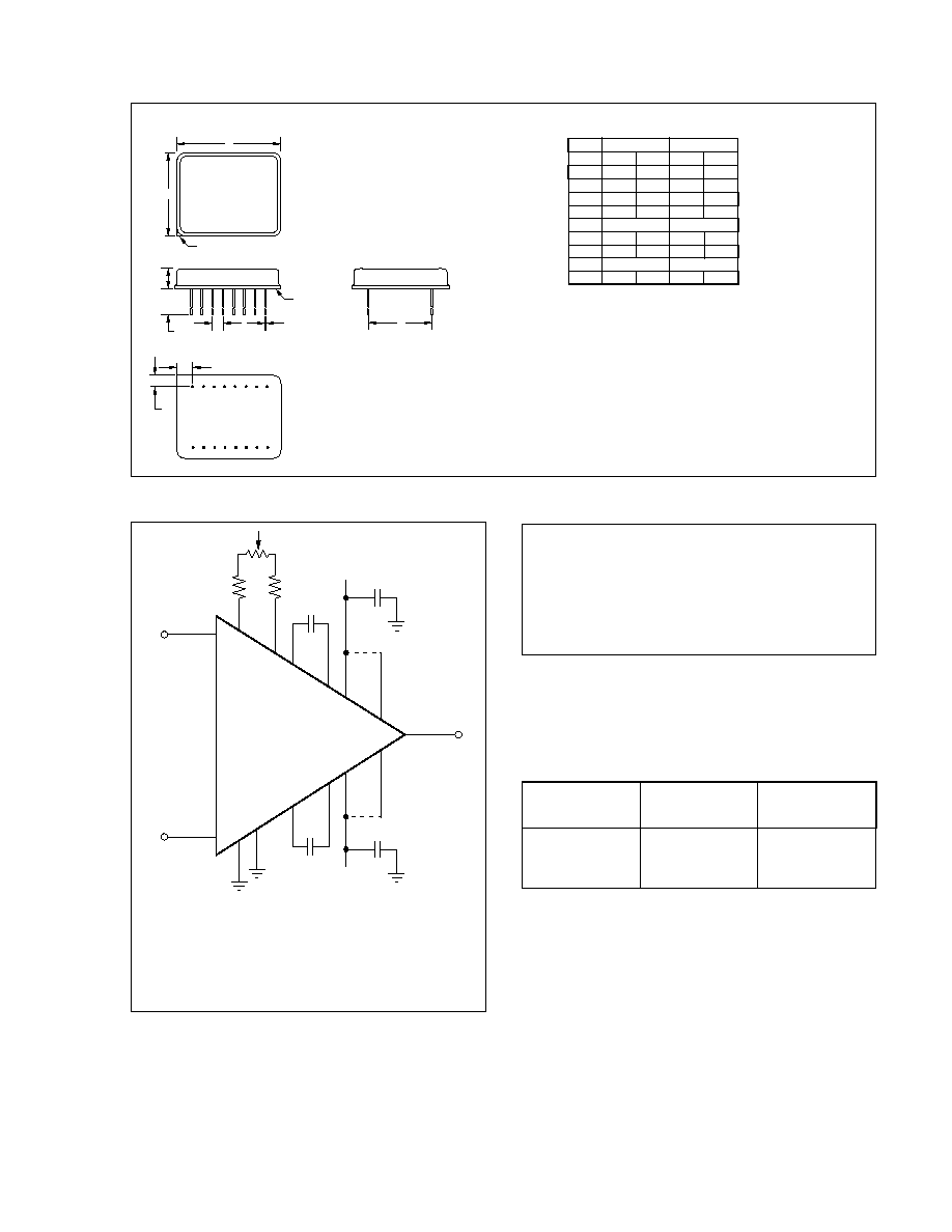
MECHANICAL
The information provided herein is believed to be reliable; however, BURR-BROWN assumes no responsibility for inaccuracies or omissions. BURR-BROWN
assumes no responsibility for the use of this information, and all use of such information shall be entirely at the user's own risk. Prices and specifications are subject
to change without notice. No patent rights or licenses to any of the circuits described herein are implied or granted to any third party. BURR-BROWN does not
authorize or warrant any BURR-BROWN product for use in life support devices and/or systems.
INCHES
MILLIMETERS
DIM
MIN
MAX
MIN
MAX
A
.963
.980
24.46
24.89
B
.760
.805
19.30
20.45
C
.175
.190
4.45
4.83
D
.014
.022
0.36
0.56
G
.100 BASIC
2.54 BASIC
H
.135
.155
3.43
3.94
K
.230
.270
5.84
6.86
L
.600 BASIC
15.24 BASIC
R
.095
.115
2.41
2.92
M Package -- 16-Pin
NOTE: Leads in true
position within 0.01"
(0.25mm) R at MMC at
seating plane.
Pin numbers shown
for reference only.
B
A
Denotes Pin 1
C
K
D
G
R
H
1
8
16
9
L
Seating
Plane
ABSOLUTE MAXIMUM RATINGS
(1)
Supply Voltage, +V
CC
to V
CC
.............................................................
±
17V
Power Dissipation, At T
CASE
+125
°
C
(2)
................................................ 1.6W
Input Voltage: Differential ....................................................................
±
V
CC
Common-Mode ............................................................
±
V
CC
Output Short Circuit Duration to Common ........................................... <5s
Temperature: pin (soldering, 20s) .................................................. +300
°
C
Junction
(1)
,T
J
........................................................... +175
°
C
Temperature Range: Storage ......................................... 65
°
C to +150
°
C
Operating (case) ........................... 55
°
C to +125
°
C
NOTES: (1) Stresses above those listed under "Absolute Maximum Ratings"
may cause permanent damage to the device. Exposure to absolute maximum
conditions for extended periods may affect device reliability. (2) Long term
operation at the maximum junction temperature will result in reduced product life.
Derate internal power dissipation to achieve high MTTF.
ORDERING INFORMATION
VOLTAGE
TEMPERATURE
OFFSET
MODEL
RANGE (
°
C)
DRIFT (
µ
V/
°
C)
OPA600BM
25 to +85
±
80
OPA600CM
25 to +85
±
20
OPA600SM
55 to +125
±
100
OPA600TM
25 to +125
±
20
CONNECTION DIAGRAM
NOTES: (1) Refer to Figure 4 for recommended frequency compensation.
(2) connect pin 9 to pin 12 and connect pin 7 to pin 6 for maximum output
current. See Application Information for further information. (3) Bypass
each power supply lead as close as possible to the amplifier pins. A 1
µ
F
CS13 tantalum capacitor is recommended. (4)There is no internal conenction.
An external connection may be made. (5) It is recommended that the
amplifier be mounted with the case in contact with a ground plane for good
thermal transfer and optimum AC performance.
Input
OPA600
C
2
C
1
V
CC
(3)
10k
16
3
2
11
14
15
12
9
8
7
6
5
4
1
+
Output
+Input
Common
(Case)
5k
5k
Current Boost
(2)
Current Boost
(2)
+V
CC
(3)
13
+V
CC
Frequency
Compensation
(1)
Offset Error
Null (optional)
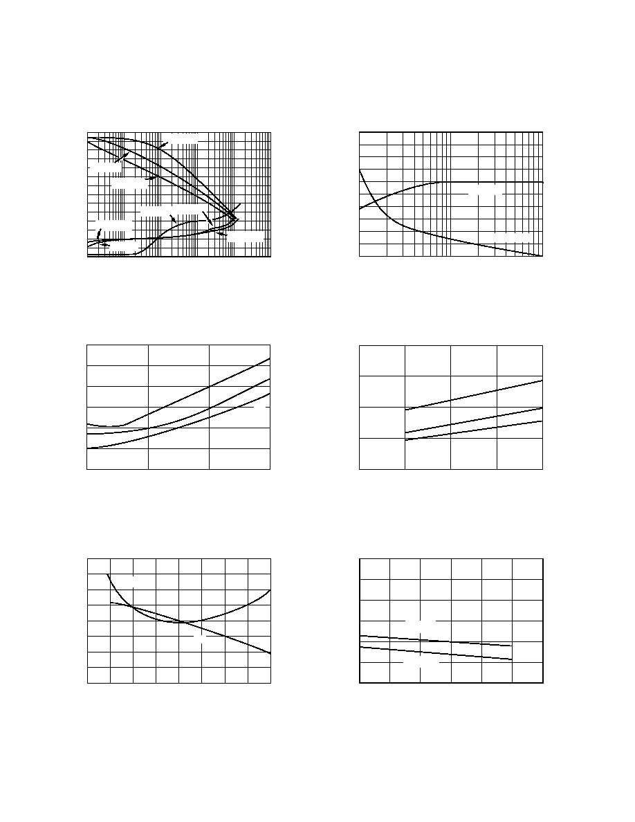
TYPICAL PERFORMANCE CURVES
Typical at T
A
= +25
°
C and
±
V
CC
= 15VDC, unless otherwise specified.
OUTPUT VOLTAGE vs OUTPUT CURRENT
30
25
20
15
10
5
0
Output Current (mA)
Output Voltage (V)
0
50
100
150
200
250
300
V
CC
= 15
V
CC
= ±12
BODE PLOT
100
90
80
70
60
50
40
30
20
10
0
10
20
30
40
Frequency (Hz)
Open-Loop Gain (dB)
10k
100k
1M
10M
100M
1000M
+100
+50
0
50
100
150
C
C
= 3.3pF
C
C
= 1pF
C
C
= 0pF
C
C
= 0pF
C
C
= 1pF
C
C
= 1pF
C
C
= 3.3pF
C
C
= 3.3pF
COMPENSATION AND SLEW RATE vs GAIN
10
8
6
4
2
0
Closed-Loop Gain (V/V) = 1 + R
F
/R
IN
Phase (Degrees)
Compensation Capacitance (pF)
1
10
100
700
600
500
400
300
200
Slew Rate (V/µs)
Compensation
Slew Rate
SETTLING TIME vs GAIN
300
250
200
150
100
50
0
Closed-Loop Gain (V/V) = 1 + R
F
/R
IN
Settling Time (ns)
1
10
100
1000
0.01%
0.1%
1%
V = 20V
SETTLING TIME AND
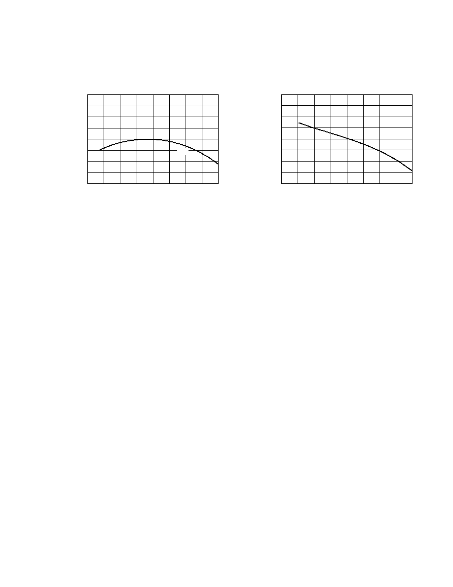
SLEW RATE vs TEMPERATURE
1.2
1.1
1.0
0.9
0.8
Temperature (°C)
Relative Value
75
50
25
0
25
50
75
100
125
t
S
t
S
(0.01%)
SR
SETTLING TIME
vs OUTPUT VOLTAGE CHANGE
200
150
100
50
0
Output Voltage Change (V)
Settling Time (ns)
0
5
10
15
20
G = 1V/V
0.01%
0.1%
1%
TYPICAL PERFORMANCE CURVES
(CONT)
Typical at T
A
= +25
°
C,
±
V
CC
= 15VDC unless otherwise specified.
INSTALLATION
AND OPERATION
WIRING PRECAUTIONS
The OPA600 is a wideband, high frequency operational
amplifier with a gain-bandwidth product exceeding 5GHz.
This capability can be realized by observing a few wiring
precautions and using high frequency layout techniques. In
general, all printed circuit board conductors should be wide
to provide low resistance, low impedance signal paths and
should be as short as possible. The entire physical circuit
should be as small as is practical. Stray capacitances should
be minimized, especially at high impedance nodes, such as
the input terminals of the amplifier and compensation pins.
Stray signal coupling from the output to the input should be
minimized. All circuit element leads should be as short as
possible and low values of resistance should be used. This
will give the best circuit performance as it will minimize the
time constants formed with the circuit capacitances and will
eliminate stray, unwanted tuned circuits.
Grounding is the most important application consideration
for the OPA600, as it is with all high frequency circuits.
Ultra-high frequency transistors are used in the design of the
OPA600 and oscillations at frequencies of 500MHz and
above can be stimulated if good grounding techniques are
not used. A ground plane is highly recommended. It should
connect all areas of the pattern side of the printed circuit that
are not otherwise used. The ground plane provides a low
resistance, low inductance common return path for all signal
and power returns. The ground plane also reduces stray
signal pickup.
Point-to-point wiring is not recommended. However, if
point-to-point wiring is used, a single-point ground should
be used. The input signal return, the load signal return and
the power supply common should all be connected at the
same physical point. This eliminates common current paths
or ground loops which can cause unwanted feedback.
Each power supply lead should be bypassed to ground as
near as possible to the amplifier pins. A 1
µ
F CS13 tantalum
capacitor is recommended. A parallel 0.01
µ
F ceramic may
be added if desired. This is especially important when
driving high current loads. Properly bypassed and modula-
tion-free power supply lines allow full amplifier output and
optimum settling time performance.
OPA600 circuit common is connected to pins 1 and 13; these
pins should be connected to the ground plane. The input
signal return, load return, and power supply common should
also be connected to the ground plane.
The case of the OPA600 is internally connected to circuit
common, and as indicated above, pins 1 and 13 should be
connected to the ground plane. Ideally, the case should be
mechanically connected to the ground plane for good ther-
mal transfer, but because this is difficult in practice, the
OPA600 should be fully inserted into the printed circuit
board with the case very close to the ground plane to make
the best possible thermal connection. If the case and ground
plane are physically connected or are in close thermal
proximity, the ground plane will provide heat sinking which
will reduce the case temperature rise. The minimum OPA600
pin length will minimize lead inductance, thereby maximiz-
ing performance.
BANDWIDTH
1.4
1.2
1.0
0.8
0.6
Temperature (°C)
Relative Value
75
50
25
0
25
50
75
100
125
G = 10V/V
OPEN-LOOP GAIN AND QUIESCENT
CURRENT vs TEMPERATURE
1.2
1.1
1.0
0.9
0.8
Temperature (°C)
Relative Value
75
50
25
0
25
50
75
100
125
I
Q
I
Q
A
VS