 | –≠–ª–µ–∫—Ç—Ä–æ–Ω–Ω—ã–π –∫–æ–º–ø–æ–Ω–µ–Ω—Ç: OPA623 | –°–∫–∞—á–∞—Ç—å:  PDF PDF  ZIP ZIP |

1
Æ
OPA623
©
1991 Burr-Brown Corporation
PDS-1132E
Printed in U.S.A. December, 1993
OPA623
OPA623
OPA623
Wide Bandwidth, Current-Feedback
OPERATIONAL AMPLIFIER
FEATURES
APPLICATIONS
q
BANDWIDTH: 350MHz, 2.8Vp-p
q
HIGH OUTPUT CURRENT:
±
70mA
q
SLEW RATE: 2100V/
µ
s, 5Vp-p
q
DIFFERENTIAL GAIN/PHASE: 0.12%/0.05
∞
q
LOW QUIESCENT CURRENT:
±
4mA
q
LOW INPUT BIAS CURRENT: 1.2
µ
A
q
RISE TIME: 1.9ns, 5Vp-p
q
SETTLING TIME: 9ns, 0.1%
q
BROADCAST/HDTV EQUIPMENT
q
HIGH-SPEED DIGITAL COMMUNICATIONS
q
PULSE/RF AMPLIFIERS
q
HIGH-SPEED ANALOG SIGNAL
PROCESSING
q
LINE DRIVING (50
, 75
)
q
DISTRIBUTION AMP
q
CRT OUTPUT STAGE DRIVER
q
ACTIVE FILTER
LARGE SIGNAL PULSE RESPONSE
Output Voltage - 5Vp-p, 5ns/DIV
Output voltage
+2.5V
OV
≠2.5V
The OPA623 operates from a
±
5V supply, is speci-
fied for the extended industrial temperature range
(≠40
∞
C to +85
∞
C), and is available in plastic SO-8
and 8-pin plastic DIP packages.
The OPA623 is a current-feedback operational ampli-
fier designed for precision wide-bandwidth systems
including high-resolution video, RF and IF circuitry,
and communications equipment.
The new circuit design, together with the complemen-
tary bipolar process, achieves performance pre-
viously unattainable in monolithic integrated circuit
technology.
The current-feedback op amp is optimized for wide
bandwidth, excellent pulse response, gain flatness,
low distortion, and operation at a low quiescent cur-
rent of
±
4mA.
It provides a 350MHz large-signal bandwidth at
2.8Vp-p output voltage, as well as a 2100V/
µ
s slew
rate. The gain flatness of 0.05dB over a 30MHz
bandwidth makes it suitable for HDTV designs. An-
other feature of the op amp is its high output current
of
±
70mA, enabling it to drive two back-terminated
75
cables when using the amplifier as a line driver in
video routers, distribution amplifiers, and analog and
digital communications equipment.
OPA623
R
2
R
1
300
R
IN
6
V
OUT
= 5.0Vp-p
300
180
≠V
CC
+V
CC
4
7
2
3
V
IN
= 2.5Vp-p
G = 1 + R
2
/R
1
= +2V/V
DESCRIPTION
Æ
International Airport Industrial Park ∑ Mailing Address: PO Box 11400, Tucson, AZ 85734 ∑ Street Address: 6730 S. Tucson Blvd., Tucson, AZ 85706 ∑ Tel: (520) 746-1111 ∑ Twx: 910-952-1111
Internet: http://www.burr-brown.com/ ∑ FAXLine: (800) 548-6133 (US/Canada Only) ∑ Cable: BBRCORP ∑ Telex: 066-6491 ∑ FAX: (520) 889-1510 ∑ Immediate Product Info: (800) 548-6132

2
Æ
OPA623
SPECIFICATIONS
DC-SPECIFICATION
OPA623AP, AU
PARAMETER
CONDITIONS
MIN
TYP
MAX
UNITS
INPUT OFFSET VOLTAGE
Initial
≠8
±
25
mV
vs Temperature
125
µ
V/
∞
C
vs Supply (tracking)
V
CC
=
±
4.5V to
±
5.5V
45
50
dB
vs Supply (non-tracking)
V
CC
= +4.5V to +5.5V
47
dB
vs Supply (non-tracking)
V
CC
= ≠4.5V to ≠5.5V
39
dB
+INPUT BIAS CURRENT
Initial
≠1.2
±
4
µ
A
vs Temperature
7
nA/
∞
C
≠INPUT BIAS CURRENT
Initial
+4.5
±
20
µ
A
vs Temperature
340
nA/
∞
C
INPUT IMPEDANCE
+Input
2.74 || 1
M
|| pF
INPUT NOISE
f = 100kHz to 100MHz
Voltage Noise Density
10
nV/
Hz
Signal-to-Noise Ratio
S/N = 0.7/(Vn ∑
5MHz)
89
dB
INPUT VOLTAGE RANGE
Common-Mode Input Range
±
3
±
3.2
V
Common-Mode Rejection
43
50
dB
RATED OUTPUT
Voltage Output
R
L
= 100
±
3
±
3.1
V
Output Current
±
70
mA
Closed-Loop Output Impedance
Gain = +2
0.12 || 1.5
|| pF
POWER SUPPLY
Rated Voltage
±
4.5
±
5.5
VDC
Derated Performance
±
4
±
6
VDC
Quiescent Current
I
O
= 0mA
±
3.5
±
4
±
4.5
mA
Rejection Ratio
45
50
dB
At V
CC
=
±
5VDC, I
Q
=
±
4mA, R
L
= 100
, R
IN
= 210
,
and T
AMB
= +25
∞
C, unless otherwise specified.
ELECTRICAL (FULL TEMPERATURE RANGE, ≠40
∞
C to +85
∞
C)
At V
CC
=
±
5VDC, I
Q
=
±
4mA, R
L
= 100
, and R
IN
= 210
,
unless otherwise specified.
INPUT OFFSET VOLTAGE
±
30
mV
BIAS CURRENT
+Input
≠1.5
±
5
µ
A
BIAS CURRENT
≠Input
27
±
50
µ
A
RATED OUTPUT
Voltage Output
R
L
= 100
±
3
±
3.1
V
POWER SUPPLY
Quiescent Current
I
O
= 0mA
±
2
±
4
±
7
mA
OPA623AP, AU
PARAMETER
CONDITIONS
MIN
TYP
MAX
UNITS
The information provided herein is believed to be reliable; however, BURR-BROWN assumes no responsibility for inaccuracies or omissions. BURR-BROWN
assumes no responsibility for the use of this information, and all use of such information shall be entirely at the user's own risk. Prices and specifications are subject
to change without notice. No patent rights or licenses to any of the circuits described herein are implied or granted to any third party. BURR-BROWN does not
authorize or warrant any BURR-BROWN product for use in life support devices and/or systems.

3
Æ
OPA623
OPA623AP, AU
PARAMETER
CONDITIONS
MIN
TYP
MAX
UNITS
SPECIFICATIONS
At V
CC
=
±
5VDC, I
Q
=
±
4mA, R
L
= 100
, R
IN
= 210
,
and T
AMB
= +25
∞
C, unless otherwise specified.
FREQUENCY DOMAIN
Large Signal
V
O
= 2.8Vp-p, Gain = +1V/V
340
MHz
Closed-Loop Bandwidth (≠3dB)
V
O
= 2.8Vp-p, Gain = +2V/V
350
MHz
V
O
= 2.8Vp-p, Gain = +5V/V
260
MHz
V
O
= 2.8Vp-p, Gain = +10V/V
210
MHz
V
O
= 2.8Vp-p, Gain = ≠1V/V
360
MHz
V
O
= 2.8Vp-p, Gain = ≠2V/V
330
MHz
V
O
= 5.0Vp-p, Gain = +2V/V
240
MHz
SMALL SIGNAL BANDWIDTH
V
O
= 0.2Vp-p, Gain = +2V/V
290
MHz
GROUP DELAY TIME
Pin 3 to Pin 6, Gain = +2V/V
1.2
ns
DIFFERENTIAL GAIN
G = +2V/V, f = 4.43MHz, R
L
= 150
V
O
= +1.4V
0.12
%
DIFFERENTIAL PHASE
G = +2V/V, f = 4.43MHz, R
L
= 150
V
O
= +1.4V
0.05
Degrees
HARMONIC DISTORTION
Gain = +2V/V
Second Harmonic
f = 10MHz, V
O
= 2.0Vp-p
≠56
dBc
Third Harmonic
≠59
dBc
Second Harmonic
f = 30MHz, V
O
= 2.0Vp-p
≠30
dBc
Third Harmonic
≠37
dBc
Second Harmonic
f = 50MHz, V
O
= 2.0Vp-p
≠30
dBc
Third Harmonic
≠33
dBc
GAIN FLATNESS PEAKING
Gain = +2V/V
V
O
= 2.0Vp-p, DC to 30MHz
0.05
dB
V
O
= 2.0Vp-p, DC to 100MHz
0.20
dB
TIME DOMAIN
Rise Time
Gain = +2V/V, 10% to 90%
V
O
= 2.0Vp-p
1.4
ns
V
O
= 5.0Vp-p
1.9
ns
Fall Time
Gain = +2V/V, 10% to 90%
V
O
= 2.0Vp-p
1.4
ns
V
O
= 5.0Vp-p
2.6
ns
SLEW RATE
Gain = +2V/V, Rise Time = 1ns
V
O
= 0.2Vp-p
140
V/
µ
s
V
O
= 5.0Vp-p
2100
V/
µ
s
SETTLING TIME
Gain = +2V/V, Rise Time = 2ns
9
ns
V
O
= 2V
p-p
, 0.1%
AC-SPECIFICATION
Power Supply Voltage .........................................................................
±
6V
Input Voltage
(1)
........................................................................
±
V
CC
±
0.7V
Operating Temperature ................................................... ≠40
∞
C to +85
∞
C
Storage Temperature ..................................................... ≠40
∞
C to +125
∞
C
Junction Temperature ................................................................... +150
∞
C
Lead Temperature (soldering, 10s) ............................................... +300
∞
C
NOTE: (1) Inputs are internally diode-clamped to
±
V
CC
.
ABSOLUTE MAXIMUM RATINGS
PACKAGE
DRAWING
TEMPERATURE
PRODUCT
PACKAGE
NUMBER
(1)
RANGE
OPA623AP
8-Pin Plastic DIP
006
≠40
∞
C to +85
∞
C
OPA623AU
SO-8 Surface Mount
182
≠40
∞
C to +85
∞
C
NOTE: (1) For detailed drawing and dimension table, please see end of data
sheet, or Appendix C of Burr-Brown IC Data Book.
PACKAGE/ORDERING INFORMATION
PIN CONFIGURATION
Top View
DIP/SO-8
NC
+V
CC
Out
8
7
6
NC
5
4
3
2
1
NC
≠In
+In
≠V
CC
ELECTROSTATIC
DISCHARGE SENSITIVITY
This integrated circuit can be damaged by ESD. Burr-Brown
recommends that all integrated circuits be handled with
appropriate precautions. Failure to observe proper handling and
installation procedures can cause damage.
ESD damage can range from subtle performance degradation to
complete device failure. Precision integrated circuits may be more
susceptible to damage because very small parametric changes
could cause the device not to meet its published specifications.

4
Æ
OPA623
INPUT PROTECTION
The need for protection from static damage has long been
recognized for MOSFET devices, but all semiconductor
devices deserve protection form this potentially damaging
source. The OPA623 incorporates on-chip ESD protection
diodes as shown in Figure 1. These diodes eliminate the
need for external protection diodes, which can add capaci-
tance and degrade AC performance.
As shown, all input pins of the OPA623 are internally
protected from ESD by a pair of back-to-back reverse-biased
diodes to either power supply. These diodes begin to con-
duct when the input voltage exceeds either power supply by
about 0.7V. This situation can occur when the amplifier
loses its power supplies while a signal source is still present.
The diodes can typically withstand a continuous current of
30mA without destruction. To ensure long-term reliability,
however, the diode current should be limited externally to
approximately 10mA whenever possible.
FIGURE 1. Internal ESD Protection.
+V
CC
≠V
CC
ESD Protection diodes internally
connected to all pins.
Internal
Circuitry
External
Pin
The internal protection diodes are designed to withstand
2.5kV (using the Human Body Model) and will provide
adequate ESD protection for most normal handling proce-
dures. However, static damage can cause subtle changes in
the amplifier input characteristics without necessarily de-
stroying the device. In precision amplifiers, such changes
may degrade offset and drift noticeably. For this reason,
static protection is strongly recommended when handling
the OPA623.

5
Æ
OPA623
TYPICAL PERFORMANCE CURVES
At V
CC
=
±
5VDC, R
L
= 100
, I
Q
=
±
4mA, R
IN
= 150
, and T
AMB
= +25
∞
C unless otherwise noted.
INPUT BIAS CURRENT vs TEMPERATURE
30
25
20
15
10
5
0
≠5
≠10
Input Bias Current (µA)
≠40
≠20
0
20
40
60
80
100
Temperature (∞C)
+Input
≠Input
OVERLOAD RECOVERY CHARACTERISTICS
Time (ns)
3
2.25
1.5
0.75
0
≠0.75
≠1.5
≠2.25
≠3
Input Voltage (V)
0
10
20
30
40
50
60
70
80
90
100
6
4.5
3
1.5
0
≠1.5
≠3
≠4.5
≠6
Output Voltage (V)
V
OUT
V
IN
G
CL
= +2V/V, V
IN
= 3.75Vp-p, R
L
= 100
, t
F
= t
R
= 1ns)
INPUT OFFSET VOLTAGE WARMUP
0
100
90
80
70
60
50
40
30
20
10
0
Time (Minutes)
1
2
3
4
5
6
7
8
9
10
Input Offset Voltage Change (µV)
AU
AP
QUIESCENT CURRENT WARMUP
100.5
100
99.5
99
98.5
98
97.5
97
96.5
96
Quiescent Current (% of final Value)
Time (minutes)
0
1
2
3
4
5
AP
AU
CLOSED-LOOP OFFSET VOLTAGE vs TEMPERATURE
0
≠2
≠4
≠6
≠8
≠10
≠12
≠14
≠16
Offset Voltage (mV)
≠40
≠20
0
20
40
60
80
100
Temperature (∞C)
QUIESCENT CURRENT vs TEMPERATURE
10
9
8
7
6
5
4
3
2
1
0
Quiescent Current (mA)
Temperature (∞C)
≠40
≠20
0
20
40
60
80
100
6
Æ
OPA623
TYPICAL PERFORMANCE CURVES
(CONT)
At V
CC
=
±
5VDC, R
L
= 100
, I
Q
=
±
4mA, R
IN
= 150
, and T
AMB
= +25
∞
C unless otherwise noted.
INPUT IMPEDANCE vs FREQUENCY
10M
1M
100k
10k
1k
100
Frequency (Hz)
1k
10k
100k
1M
10M
100M
1G
Input Impedance (
)
OPEN-LOOP GAIN vs FREQUENCY
Frequency (Hz)
Open-Loop Gain (dB)
60
50
40
30
20
10
0
≠10
≠20
≠30
≠40
300k
1M
10M
100M
1G
3G
OPA623
3
2
6
100
V
OUT
180
V
IN
+
≠
100k
1M
10M
100M
Frequency (Hz)
Output Impedance (
)
OUTPUT IMPEDANCE vs FREQUENCY
10k
51
OPA623
300
3
2
6
50
300
0dB
230
+
≠
100
10
1
0.1
1G
Frequency (Hz)
Delay Time (ns)
GROUP DELAY TIME
3
2
1
0
≠1
≠2
≠3
≠4
≠5
≠6
≠7
1M
10M
100M
300k
50
OPA623
3
2
6
50
V
IN
180
300
V
OUT
Group Delay Time
+
≠
300
SMALL SIGNAL PULSE RESPONSE
Time (ns)
160
120
80
40
0
≠40
≠80
≠120
≠160
Output Voltage (mV)
0
10
20
30
40
50
60
70
80
90
100
G
CL
= +2V/V, V
OUT
= 0.2Vp-p, t
RISE
= t
FALL
= 1ns (Generator)
SMALL SIGNAL PULSE RESPONSE
Time (ns)
160
120
80
40
0
≠40
≠80
≠120
≠160
Output Voltage (mV)
0
10
20
30
40
50
60
70
80
90
100
G
CL
= +10V/V, V
OUT
= 0.2Vp-p, t
RISE
= t
FALL
= 1ns(Generator)

7
Æ
OPA623
TYPICAL PERFORMANCE CURVES
(
CONT)
At V
CC
=
±
5VDC, R
L
= 100
, I
Q
=
±
4mA, R
IN
= 150
, and T
AMB
= +25
∞
C unless otherwise noted.
LARGE SIGNAL PULSE RESPONSE
Time (ns)
Output Voltage (V)
0
10
20
30
40
50
60
70
80
90
100
G
CL
= +2V/V, V
OUT
= 5Vp-p, t
RISE
= t
FALL
= 1ns (Generator)
4
3
2
1
0
≠1
≠2
≠3
≠4
LARGE SIGNAL PULSE RESPONSE
Time (ns)
4
3
2
1
0
≠1
≠2
≠3
≠4
Output Voltage (V)
0
10
20
30
40
50
60
70
80
90
100
G
CL
= +10V/V, V
OUT
= 5Vp-p, t
RISE
= t
FALL
= 1ns(Generator)
15
10
5
0
≠5
≠10
≠15
≠20
≠25
1M
10M
100M
1G
Frequency (Hz)
Output Voltage (Vp-p)
BANDWIDTH vs OUTPUT VOLTAGE
20
dB
300k
0.2Vp-p
1.4Vp-p
2.8Vp-p
5Vp-p
G
CL
= +1V/V
0.6Vp-p
3G
15
10
5
0
≠5
≠10
≠15
≠20
≠25
1M
10M
100M
1G
Frequency (Hz)
Output Voltage (Vp-p)
BANDWIDTH vs OUTPUT VOLTAGE
20
dB
300k
0.2Vp-p
1.4Vp-p
2.8Vp-p
5Vp-p
G
CL
= +2V/V
0.6Vp-p
3G
15
10
5
0
≠5
≠10
≠15
≠20
≠25
1M
10M
100M
3G
Frequency (Hz)
Output Voltage (Vp-p)
BANDWIDTH vs OUTPUT VOLTAGE
20
dB
300k
1G
5Vp-p
2.8Vp-p
1.4Vp-p
0.6Vp-p
0.2Vp-p
G
CL
= +10V/V
15
10
5
0
≠5
≠10
≠15
≠20
≠25
1M
10M
100M
1G
Frequency (Hz)
Output Voltage (Vp-p)
BANDWIDTH vs OUTPUT VOLTAGE
20
dB
300k
3G
G
CL
= ≠2V/V
0.2Vp-p
0.6Vp-p
1.4Vp-p
2.8Vp-p
5Vp-p

8
Æ
OPA623
0
≠10
≠20
≠30
≠40
≠50
≠60
≠70
≠80
≠90
Frequency (Hz)
HARMONIC DISTORTION vs FREQUENCY
1M
10M
100M
Harmonic Distortion (dBc)
3f
2f
TYPICAL PERFORMANCE CURVES
(CONT)
At V
CC
=
±
5VDC, R
L
= 100
, I
Q
=
±
4mA, R
IN
= 150
, and T
AMB
= +25
∞
C unless otherwise noted.
1M
10M
100M
1G
Frequency (Hz)
Gain (5dB/Div)
FREQUENCY RESPONSE vs C
LOAD
G
CL
= +2V/V, V
IN
= 1.4Vp-p
10pF
22pF
47pF
100k
2pF
51
DUT
50
R
2
C
L
R
1
3
2
6
R
1
300
270
240
120
R
2
300
270
240
120
C
L
2pF
10pF
22pF
47pF
3
2
1
0
≠1
≠2
≠3
≠4
≠5
1M
10M
100M
1G
Frequency (Hz)
Gain (dB)
GAIN FLATNESS
4
≠6
100k
G
CL
= +2V/V, V
IN
= 1.0Vp-p
≠3dB
AVERAGE SUPPLY CURRENT vs FREQUENCY
10k
100k
1M
10M
100M
1G
Frequency (Hz)
50
45
40
35
30
25
20
15
10
5
0
Average Supply Current I
Q
(mA)
Sine Curve
R
L
= 100
G = +2V/V
C
L
= 2pF
2.8Vp-p
1.4Vp-p
0.2Vp-p
5.0Vp-p
1M
10M
100M
3G
Gain (5dB/DIV)
FREQUENCY RESPONSE vs R
LOAD
100k
G
CL
= +2V/V, R
1
= R
2
= 300
, V
IN
= 1.0Vp-p
1G
50
100
200
500
Frequency (Hz)
SPECTRAL NOISE VOLTAGE DENSITY
100
10
1
Frequency (Hz)
Voltage Noise nV/
Hz
100
1k
10k
100k
1M
10M

9
Æ
OPA623
DISCUSSION OF
PERFORMANCE
Requiring very low quiescent power, the OPA623 achieves
its exceptional AC performance by using the current-feed-
back topology. This wide-band monolithic operational am-
plifier is designed for gain applications of up to 20V/V,
where power and cost are of primary concern.
Operating from a
±
5V supply, the OPA623 consumes only
40mW, yet maintains a 350MHz large-signal bandwidth at
V
OUT
= 2.8Vp-p and a 2100V/
µ
s slew rate. Benefiting
from the current-feedback architecture, the OPA623 offers
stable operation with no compensation capacitor, even at
unity gain.
With its low differential gain and phase errors of typically
0.12% and 0.05
∞
at 4.43MHz, the OPA623 meets the perfor-
mance and cost requirements of high-volume broadcast and
HDTV applications.
The OPA623's large-signal bandwidth, high slew rate,
excellent pulse response, and high drive capabilities are
features well-suited to wide-band RGB video applica-
tions, RF instruments, and even high-speed digital com-
munication systems.
For most circuit configurations, the OPA623 current-
feedback op amp can be treated like a conventional op
amp. As with a voltage-feedback op amp, the feedback
network connected to the inverting input controls the
closed-loop gain. But with a current-feedback op amp, the
impedance of the feedback network also controls the
open-loop gain and frequency response. Feedback resis-
tor values can be selected to provide nearly constant
closed-loop bandwidth over a wide range of gains and flat
gain adjustment vs frequency.
DESCRIPTION
A wide-band operational transconductance amplifier (OTA)
and an output buffer are the main blocks of a current-
feedback op amp. The simplified circuit diagram is illus-
trated in Figure 2. The OTA consists of a complementary
unity-gain amplifier and a subsequent current mirror. The
input buffer is connected across the inputs of the op amp.
The voltage at the high-impedance +In terminal is trans-
ferred to the ≠In terminal at a low impedance. The current
mirrors reflect any current flowing into or out of the +In
terminal by a fixed ratio to the high-impedance OTA output,
which is directly connected to the complementary output
buffer. It is designed to drive low-impedance transmission
FIGURE 2. Simplified Circuit Diagram.
+In
3
2
6
V
OUT
≠V
CC
= ≠5V
4
7
+V
CC
= +5V
OTA
BUFFER
Bias
Circuitry
≠In

10
Æ
OPA623
FIGURE 3. Non-Inverting Current-Feedback Op Amp Configuration.
B
1
≠V
CC
V
IN
+V
CC
R
IN
+In
≠In
R
1
R
2
Out
V
OUT
7
3
4
2
6
lines or loads. The buffer output is not current-limited or
protected.
As can be seen in Figure 3, the feedback in the form of a
current is applied through R
2
to the low-impedance inverting
input, and the size of R
2
||
R
1
determines the open-loop gain
of the op amp.
The hybrid model shown in Figure 4 describes the AC
behavior of a wide-band current-feedback op amp that is not
internally compensated. The open-loop frequency response,
which is illustrated in Figure 5 for various R
2
values, is
determined by two time constants. The elements R and C
between the current source output and the output buffer form
the dominant open-loop pole T
C
. The signal delay time T
D
modelled in the output buffer combines several small phase-
shifting time constants and delay times. They are distributed
throughout the amplifiers and are also present in the feed-
back loop. As shown in Figure 5, increasing R
2
|| R
1
leads to
a decreasing open-loop gain. The ratio of the two time
constants T
C
and T
D
also determines the product G
OL
∑ G
CL
for optimal closed-loop frequency response:
FIGURE 4. Hybrid Model OPA623.
≠1
R
2
R
1
g
m
+In
3
2
6
R
T
C
T
Out
T
D
≠In
provides a nearly constant closed-loop bandwidth, as shown
in Figure 6 for various gains with an optimal flat frequency
response. This behavior stands in contrast to op amps that
are internally compensated for stable unity-gain operation,
where the bandwidth is inversely proportional to the closed-
loop gain, sharply limiting the bandwidth and slew rate at
high output levels and gains.
In general, lower feedback resistors produce wider band-
width, more frequency response peaking, and more pulse
response overshooting. Higher feedback resistors results in
an overdamped response with little or no peaking and
overshooting.
Component pin and layout capacitances together with trace
and wire board inductances from a resonant IC circuit can
lead to oscillations of several hundreds of MHz. This very
high frequency oscillation leads to an excessive increase in
supply current which can destroy the device.
A resistor (100
to 250
) in series and close to the high-
impedance, non-inverting input damps the LC circuit and
generates a safe operation.
THERMAL CONSIDERATIONS
The OPA623 does not require a heat sink for operation in
most environments. The use of a heat sink, however, will
The two time constants T
C
and T
D
, however, are fixed by the
op amp design. But varying R
2
|| R
1
externally in the
feedback loop allows for variation of the open-loop gain
G
OL
versus the closed-loop gain G
CL
. This keeps the product
G
OL
* G
CL
constant, which is the theoretical condition for
optimally flat frequency response.
This variation may be beneficial when driving high capaci-
tive loads. Setting the open-loop gain externally also allows
the circuit to be optimized to a wide range of capacitive
loads, as shown in Figure 7 for a closed-loop gain of
+2V/V and a capacitive load of up to 47pF.
It should be noted here that higher open-loop gain (resulting
from lower feedback resistors) also yields lower distortion.
With external control of the open-loop characteristics of the
op amp, dynamic behavior can be tailored to individual
application requirements, and the open-loop gain selection
T
C
2T
D
+
G
OL
= G
CL
∑

11
Æ
OPA623
reduce the internal thermal rise, resulting in cooler, more
reliable operation. At extreme temperatures and under full
load conditions a heat sink is necessary. The internal power
dissipation is given by the equation P
D
= P
DQ
+ P
DL
, (P
DQ
is the quiescent power dissipation and P
DL
is the power
dissipation in the output stage due to the load). Although the
P
DQ
is very low (40mW at V
CC
=
±
5V), care should be taken
when a signal is applied. For high-speed op amps, a more
precise approach to determine power consumption is to
measure the average total quiescent current for several
typical load conditions. The power consumption of the
OPA623 is influenced by the kind of signal, the applied
signal frequency, the output voltage, load resistor, and the
repetition rate of the signal transitions. Figure 8 shows the
average supply current versus the frequency of an applied
sine wave for various output voltages. Figure 9 illustrates the
average supply current versus the repetition frequency of an
applied square wave signal.
FIGURE 5. Open-Loop Gain vs R
2
|| R
1
.
50
40
30
20
10
0
≠10
≠20
≠30
Frequency (Hz)
Open-Loop Gain (dB)
100k
1M
10M
100M
1G
300
150
27
1M
10M
100M
1G
Frequency (Hz)
Gain (5dB/Div)
FREQUENCY RESPONSE vs C
LOAD
G
CL
= +2V/V, V
IN
= 1.4Vp-p
10pF
22pF
47pF
100k
2pF
51
DUT
50
R
2
C
L
R
1
3
2
6
R
1
300
270
240
120
R
2
300
270
240
120
C
L
2pF
10pF
22pF
47pF
FIGURE 7. Frequency Response vs C
LOAD
.
10k
100k
1M
10M
100M
1G
Frequency (Hz)
50
45
40
35
30
25
20
15
10
5
0
Average Supply Current I
Q
(mA)
Sine Curve
R
L
= 100
G = +2V/V
C
L
= 2pF
5.0Vp-p
2.8Vp-p
1.4Vp-p
0.2Vp-p
FIGURE 8. Average Supply Current vs Frequency
(sinewave).
FIGURE 6. Optimum Frequency Response vs Closed-Loop
Gain.
20
15
10
5
0
≠5
≠10
≠15
≠20
≠25
≠30
Gain (5dB/DIV)
Frequency (Hz)
100k
1M
10M
100M
1G
+10V/V
+2V/V
+1V/V
≠1V/V
25
20
15
10
5
0
Average Supply Current I
Q
(mA)
10k
100k
1M
10M
100M
Frequency (Hz)
5.0Vp-p
2.8Vp-p
1.4Vp-p
0.2Vp-p
G = +2V/V
C
L
= 2pF
R
L
= 100
FIGURE 9. Average Supply Current vs Frequency
(squarewave).

12
Æ
OPA623
CIRCUIT LAYOUT
The high-frequency performance of the operational ampli-
fier OPA623 can be greatly affected by the physical layout
of the printed circuit board. The following tips are offered as
suggestions. Oscillations, ringing, poor bandwidth and set-
tling, and peaking are all typical problems that plague high-
speed components when they are used incorrectly.
∑ A resistor (100
to 250
) in series and close to the high-
impedance, noninverting input is necessary to reduce
peaking; this resistor prevents any very high-frequency
oscillations at the op amp input, which can lead to an
excessive increase in quiescent current.
∑ Bypass power supplies very close to the device pins. Use
tantalum chip capacitors (approximately 2.2
µ
F) with a
parallel 470pF ceramic chip capacitor. Surface-mount
types are recommended because of their low lead induc-
tance. Although the OPA623 operates at a low quiescent
current, high charging and discharging currents flow
during steep transitions.
∑ PC board traces for power lines should be wide to reduce
impedance and inductance.
∑ Make short low-inductance traces. The entire physical
circuit should be as small as possible.
∑ Use a low-impedance ground plane on the component
side to ensure that low-impedance ground is available
throughout the layout, however, do not extend the ground
plane under high-impedance nodes such as the amplifier's
input terminals, which are sensitive to stray capacitances.
∑ Sockets are not recommended because they add signifi-
cant inductance and parasitic capacitance.
∑ Use low-inductance, surface-mounted components. Cir-
cuits using all surface-mount components with the
OPA623AU will offer the best AC performance.
∑ Plug-in prototype boards and wire-wrap boards will not
function well. A clean layout using RF techniques is
essential--there are no shortcuts.
∑ Make the feedback trace as short as possible. The invert-
ing input is sensitive to stray capacitances that lead to
peaking in the frequency response. A stray capacitance at
the inverting input increases the gain at high frequencies.
FIGURE 10. Circuit Schematic for Non-inverting and Inverting Configuration. Refer to Table I for Resistor Values.
OPA623AP
OPA623AU
GAIN
GAIN
COMPONENT
≠2
≠1
+1
+2
+5
+10
≠2
≠1
+1
+2
+5
+10
R
i
150
150
200
180
100
100
150
150
270
180
100
100
R
1
390
390
360
300
300
130
390
390
470
300
300
160
R
2
--
--
--
300
75
15
--
--
--
300
76
18
R
N1
200
390
--
--
--
--
200
390
--
--
--
--
R
N2
68
56
--
--
--
--
68
56
--
--
--
--
Typical
Bandwidth (MHz)
V
OUT
= 0.2Vp-p
200
--
320
290
--
170
200
--
320
290
--
170
V
OUT
= 2.8Vp-p
330
360
340
350
260
210
330
360
340
350
260
210
TABLE I. Recommended Component Values.
Non Inverting
R
O
50
OPA623
R
3
50
3
2
6
R
i
R
1
Out
In≠
R
N2
4
7
R
2
In+
Inverting
R
O
50
OPA623
3
2
6
R
i
R
1
Out
4
7
R
N1
+5V
Gnd
≠5V
C2
470pF
C4
10nF
C6
2.2µF
C1
470pF
C3
10nF
C5
2.2µF
7
4

13
Æ
OPA623
APPLICATIONS INFORMATION
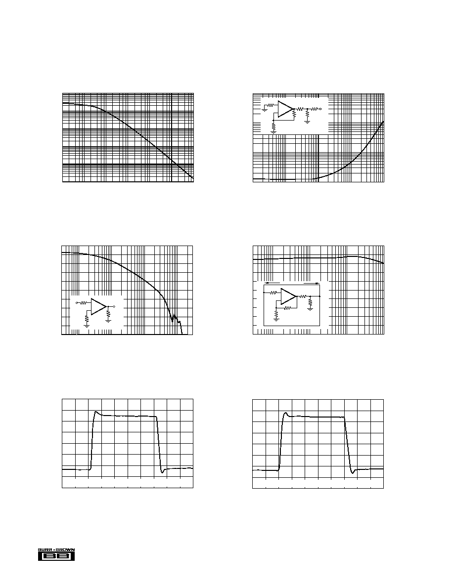
The precise pulse response and high slew rate enables the
OPA623 to be used in digital communication systems.
Figure 12 shows the circuit schematic of an output amplifier
with a gain of +2V/V, which can drive a 75
coaxial cable
with a high-speed data stream of 140Mbit/s. Figure 13, for
a binary 0, and Figure 14, for a binary 1, shows the pulse
masks of the CCITT recommendation G.703 and the corre-
sponding pulse responses of the OPA623. The signal code at
the file rate of 139.264Mbit/s is CMI, the signal amplitude
is 1Vp-p with
±
11dB amplitude limits. Naturally, the OPA623
can also be used for HDB3 encoded 34Mbit/s,155Mbit/s,
STM-1, and 155Mbit/s B-ISDN transmission systems.
FIGURE 12. Driver Amplifier for a Digital 140Mbit/s
Transmission system.
FIGURE 13. Mask of a Pulse Corresponding to a Binary 0 per CCITT Recommendation G.703.
0.60
0.55
0.50
0.45
0.40
0.05
≠0.05
≠0.40
≠0.45
≠0.50
≠0.55
≠0.60
V
1ns
0.1ns
0.1ns
Nominal
zero level
(2)
= Note 1.
Negative
transitions
Positive transition
at mid-unit interval
1ns
1ns
1ns
1.795ns
1.795ns
T = 7.18ns
1.795ns
1ns
1ns
1.795ns
Nominal
Pulse
0.1ns
0.1ns
0.35ns
0.35ns
NOTE: (1) The maximum "steady state" amplitude should not exceed the 0.55V limit. Overshoots and other transients are permitted to fall
into the dotted area, bounded by the amplitude levels 0.55V and 0.6V, provided that they do not exceed the steady state level by more
than 0.05V. The possibility of relaxing the amount by which the overshoot may exceed the steady state level is under study.
(2) For all measurements using these masks, the signal should be AC coupled, using a capacitor of not less than 0.01µF, to the input of
the oscilloscope used for measurements.
The nominal zero level for both masks should be aligned with the oscilloscope trace with no input signal. With the signal then applied, the
vertical position of the trace can be adjusted with the objective of meeting the limits of the masks. Any such adjustment should be the
same for both masks and should not exceed
±
0.05V. This may be checked by removing the input signal again and verifying that the trace
lies within
±
0.05V of the nominal zero level of masks.
(3) Each pulse in a coded pulse sequence should meet the limits of the relevant mask, irrespective of the state of the preceding and
succeeding pulses. For actual verification, if a 139264kHz timing signal associated with the source of the interface signal is available, its
use as a timing reference for an oscilloscope is preferred. Otherwise, compliance with the relevant mask may be tested by means of all-0s
and all-1s signals, respectively. (In practice, the signal may contain frame alignment bits per Rec. G.751.)
(4) For the purpose of these masks, the rise time and decay time should be measured between ≠0.4V and 0.4V, and should not exceed
2ns.
OPA623
R
2
R
1
300
R
IN
6
V
OUT
300
180
≠V
CC
+V
CC
4
7
2
3
≠In
+In
V
IN
G = 1 + R
2
/R
1
= +2V/V

14
Æ
OPA623
FIGURE 14. Mask of a Pulse Corresponding to a Binary 1 per CCITT Recommendation G.703.
0.60
0.55
0.50
0.45
0.40
0.05
≠0.05
≠0.40
≠0.45
≠0.50
≠0.55
≠0.60
V
1ns
0.1ns
Nominal
zero level
(2)
= Note 1.
Negative
transition
Positive transition
1ns
1ns
1.795ns
T = 7.18ns
1.795ns
3.59ns
1.35ns
1.35ns
3.59ns
1ns
0.5ns
Nominal
Pulse
0.5ns
0.1ns
NOTE: (1) The maximum "steady state" amplitude should not exceed the 0.55V limit. Overshoots and other transients are permitted to
fall into the dotted area, bounded by the amplitude levels 0.55V and 0.6V, provided that they do not exceed the steady state level by
more than 0.05V. The possibility of relaxing the amount by which the overshoot may exceed the steady state level is under study.
(2) For all measurements using these masks, the signal should be AC coupled, using a capacitor of not less than 0.01µF, to the input of
the oscilloscope used for measurements.
The nominal zero level for both masks should be aligned with the oscilloscope trace with no input signal. With the signal then applied,
the vertical position of the trace can be adjusted with the objective of meeting the limits of the masks. Any such adjustment should be
the same for both masks and should not exceed
±
0.05V. This may be checked by removing the input signal again and verifying that the
trace lies within
±
0.05V of the nominal zero level of masks.
(3) Each pulse in a coded pulse sequence should meet the limits of the relevant mask, irrespective of the state of the preceding and
succeeding pulses. For actual verification, if a 139264kHz timing signal associated with the source of the interface signal is available, its
use as a timing reference for an oscilloscope is preferred. Otherwise, compliance with the relevant mask may be tested by means of all-
0s and all-1s signals, respectively. (In practice, the signal may contain frame alignment bits per Rec. G.751.)
(4) For the purpose of these masks, the rise time and decay time should be measured between ≠0.4V and 0.4V, and should not exceed
2ns.
(5) The inverse pulse will have the same characteristics. Note that the timing tolerance at the zero level of the negative and positive
transitions are ±0.1ns and ±0.5n, respectively.
15
Æ
OPA623
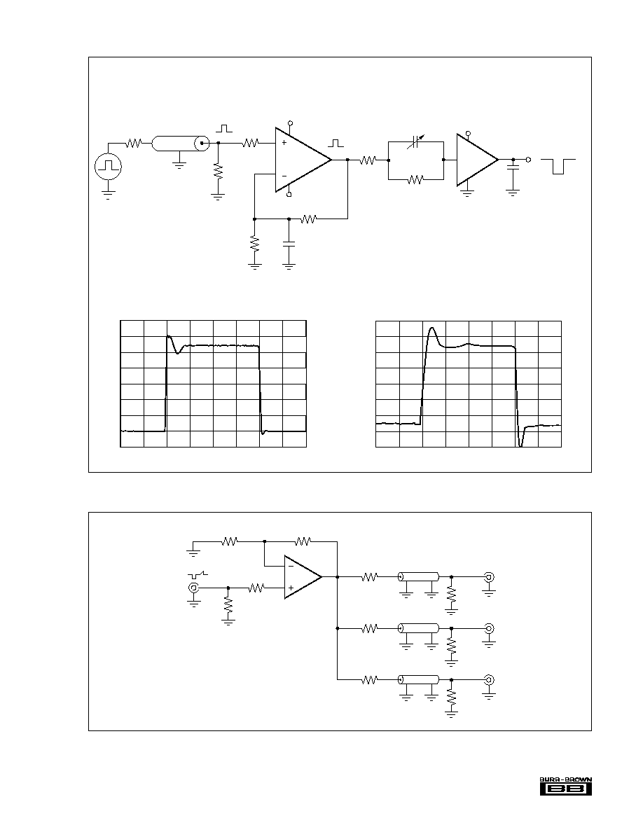
330
75
OPA623
330
75
V
OUT
75
75
V
OUT
75
75
V
OUT
75
2
6
3
High output current drive capability (6Vp-p
into 50
) allows three back-terminated 75
transmission lines to be simutaleously driven.
Video
Input
75
Transmission Line
150
FIGURE 15. Video Amplifier for High Resolution Monitor (1600
x
1200 pixel).
FIGURE 16. Video Distribution Amplifier.
OPA623
t
RISE
= 3.0ns
t
FALL
= 2.3ns
50Vp-p
12pF
9
+80V; 60mA
287
50pF
t
RISE
= 1.85ns
t
FALL
= 1.95ns
24
4Vp-p
6
7
+5V
3
2
4
≠5V
470
6.8pF
120
50
150
50
0.8Vp-p
0
t
RISE
= 0.7ns
t
FALL
= 0.7ns
Pulse
Generator
CR3425
1
V
OUT
C
LOAD
V
OUT
OPA623 4Vp-p
10ns/div
750mV/div
V
OUT
CR3425 50Vp≠p
10ns/div
10V/div