 | –≠–ª–µ–∫—Ç—Ä–æ–Ω–Ω—ã–π –∫–æ–º–ø–æ–Ω–µ–Ω—Ç: OPA63xU | –°–∫–∞—á–∞—Ç—å:  PDF PDF  ZIP ZIP |
R
4
R
2
R
3
R
7
R
11
R
12
R
13
Out
J
2
3
4
7
6
5
8
2
R
1
R
6
IN
J
1
R
5
C
4
C
6
C
5
C
7
1
GND
+V
S
≠V
S
P
1
C
3
C
2
+
L
2
L
1
C
1
+
R
8
R
9
V
L
J
4
R
10
V
H
/DIS/DIS
J
3
1
2
3
4
8
7
6
5
NC
≠In
+In
≠V
S
NC
+V
S
Output
NC
PRODUCT
PIN #2
PIN #5
PIN #8
OPA63xU
--
--
DIS
OPA64xU
--
≠V
S
(optional)
+V
S
(optional)
OPA628U
--
≠V
S
+V
S
OPA680U
--
--
DIS
OPA681U
--
--
DIS
OPA682U
R
G
--
DIS
OPA686U
--
--
DNC
(1)
OPA688U
--
V
L
V
H
OPA689U
--
V
L
V
H
NOTE: (1) DNC means do not connect.
Æ
© 1998 Burr-Brown Corporation
LI-513A
Printed in U.S.A. November, 1999
DEM-OPA68xU
EVALUATION FIXTURE
DESCRIPTION
The DEM-OPA68xU demonstration board is an
unpopulated printed circuit board (PCB) for Burr-
Brown's high speed single op amps available in SO-8
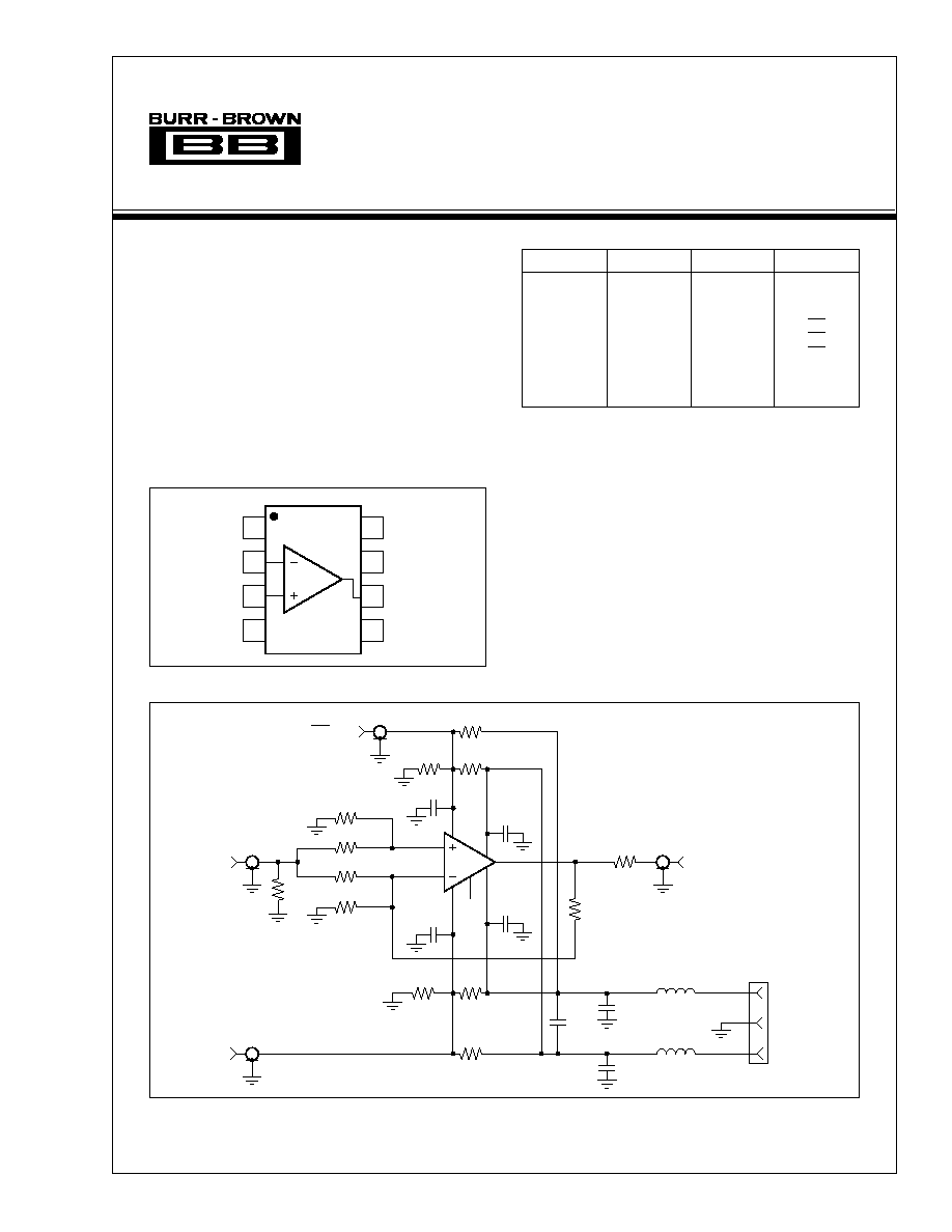
packages. Figure 1 shows the pin out used for most of
these op amps. Table I lists the exceptions to this pin-out
that are also supported by this board. For more informa-
tion on these op amps, and good PCB layout techniques,
see the individual data sheets.
The ordering number for this board is MKT-351. Limit
of 5 per customer.
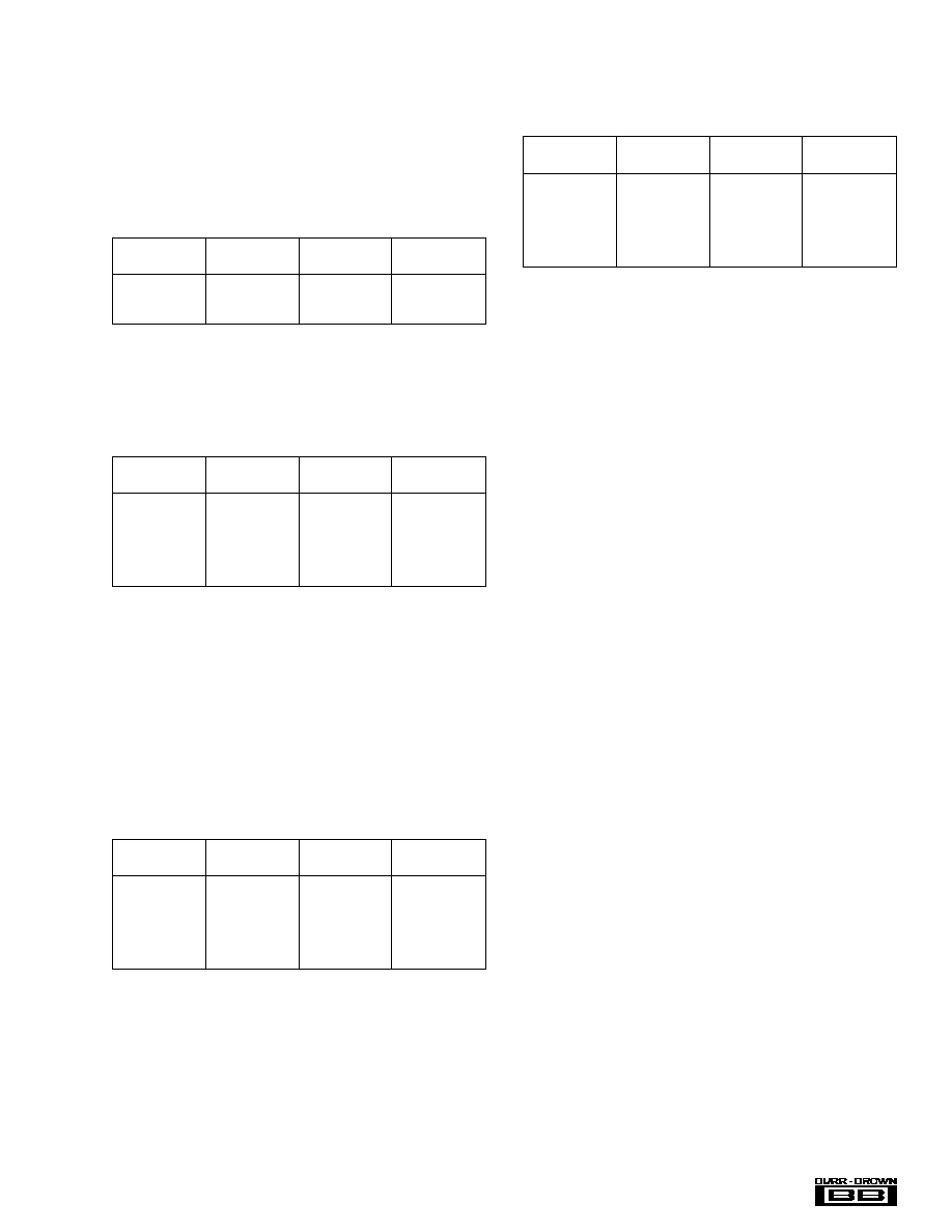
FIGURE 2. Circuit Schematic for DEM-OPA68xU.
Top View
SO-8
FIGURE 1. Pin Configuration for OPA6xxU.
TABLE I. Supported Exceptions to Pinout in Figure 1.
CIRCUIT
The circuit schematic in Figure 2 shows the connec-
tions for all possible components. Each model will
only use some of the components.
COMPONENTS
Components that have RF performance similar to the
ones in Table II may be substituted. C
1
and C
2
need a
larger voltage rating for
±
15V dual supplies.
International Airport Industrial Park ∑ Mailing Address: PO Box 11400, Tucson, AZ 85734 ∑ Street Address: 6730 S. Tucson Blvd., Tucson, AZ 85706 ∑ Tel: (520) 746-1111
Twx: 910-952-1111 ∑ Internet: http://www.burr-brown.com/ ∑ Cable: BBRCORP ∑ Telex: 066-6491 ∑ FAX: (520) 889-1510 ∑ Immediate Product Info: (800) 548-6132

2
Æ
DEM-OPA68xU
PART
DESCRIPTION
C
1
, C
2
Tantalum Chip Capacitor, SMD EIA size 3528, 20V
C
3
- C
7
Multi-Layer Ceramic Chip Cap., SMD 1206, 50V
J
1
- J
4
SMA or SMB Board Jack (Amphenol 901-144-8)
L
1
, L
2
EMI-Suppression Ferrite Chip, SMD 1206
(Steward LI 1206 B 900 R)
P
1
Terminal Block, 3.5mm centers
(On-Shore Technology ED555/3DS)
R
1
- R
13
Metal Film Chip Resistor, SMD 1206, 1/8W
TABLE II. Component Descriptions.
R
1
and R
7
set the I/O impedance, R
2
- R
6
set the gain, and C
1
- C
5
are supply bypass capacitors. C
3
is optional; it adds a
bypass between the supplies, which improves distortion
performance for some models. L
1
and L
2
are ferrite chips
that can reduce interactions with the power supply at high
frequencies. If not desired, they can be replaced with 0
resistors. R
8
- R
13
, C
6
and C
7
are optional components that
support op amps with special functions (see Table I).
For single supply operation, do not connect L
2
; otherwise,
the ≠V
S
input to P
1
would be at ground potential.
Standard Current-Feedback Op Amps--These op amps
have the pinout shown in Figure 1. Table III shows typical
values used for these parts. To select component values for
your op amp (especially R
6
), consult its data sheet.
DUAL SUPPLY
DUAL SUPPLY
SINGLE SUPPLY
COMPONENT
(G = +2)
(G = ≠1)
(G = +1)
R
1
49.9
57.6
49.9
R
2
10.0
Open
10.0
R
3
Open
10.0
Open
R
4
Open
402
Open
R
5
402
Open
Open
R
6
402
402
402
R
7
49.9
49.9
49.9
R
8
- R
13
Open
Open
Open
C
1
2.2
µ
F
2.2
µ
F
2.2
µ
F
C
2
2.2
µ
F
2.2
µ
F
Open
C
3
0.01
µ
F
0.01
µ
F
Open
C
4
0.1
µ
F
0.1
µ
F
0
C
5
0.1
µ
F
0.1
µ
F
0.1
µ
F
C
6
, C
7
Open
Open
Open
NOTE: The values and gains shown will not work for all current-feedback op
amps. See the data sheet to select proper values. The I/O impedances are 50
.
DUAL SUPPLY
DUAL SUPPLY
SINGLE SUPPLY
COMPONENT
(G = +2)
(G = ≠1)
(G = +1)
R
1
49.9
57.6
49.9
R
2
178
Open
0
R
3
Open
210
Open
R
4
Open
402
Open
R
5
402
Open
Open
R
6
402
402
24.9
R
7
49.9
49.9
49.9
R
8
- R
13
Open
Open
Open
C
1
2.2
µ
F
2.2
µ
F
2.2
µ
F
C
2
2.2
µ
F
2.2
µ
F
Open
C
3
0.01
µ
F
0.01
µ
F
Open
C
4
0.1
µ
F
0.1
µ
F
0
C
5
0.1
µ
F
0.1
µ
F
0.1
µ
F
C
6
, C
7
Open
Open
Open
NOTE: The values and gains shown will not work for all voltage-feedback op
amps. See the individual op amp data sheet to select proper values. The I/O
impedances are 50
.
TABLE IV. Standard Voltage-Feedback Op Amps.
TABLE V. OPA628U and OPA64xU Changes.
DUAL SUPPLY
DUAL SUPPLY
SINGLE SUPPLY
COMPONENT
(G = )+2
(G = ≠1)
(G = +1)
R
8
,
R
11
0
0
0
C
1
4.7
µ
F
4.7
µ
F
4.7
µ
F
C
2
4.7
µ
F
4.7
µ
F
Open
C
4
,
C
6
0.1
µ
F
0.1
µ
F
0
C
5
,
C
7
0.1
µ
F
0.1
µ
F
0.1
µ
F
OPA63xU--Pin 8 disables the output when high (OPA632
and OPA635). Table VII shows different ways to set up pin
8's voltage using R
8
, R
9
and C
7
. Use Table IV for the other
components, except for the changes shown in Table VI; note
these are all single supply configurations.
SINGLE SUPPLY SINGLE SUPPLY SINGLE SUPPLY
COMPONENT
(G = +2)
(G = ≠1)
(G = +1)
C
4
0
0
0
TABLE VI. OPA63xU Changes.
TABLE III. Standard Current-Feedback Op Amps.
Standard Voltage-Feedback Op Amps--These op amps
have the pinout shown in Figure 1. Table IV shows typical
values used for these parts. To select component values for
your op amp, consult its data sheet.
OPA628U and OPA64xU--These op amps have additional
supply pins (see Table I) to improve distortion. Use the
values in Table IV, except for the changes shown in Table
V (the OPA64xP family will function without these changes,
but with reduced distortion performance).
CONFIGURATION
R
8
C
9
External Source
Open
49.9
On
Open
0
Off
0
Open
CONFIGURATION
R
8
R
9
C
7
External Source
Open
49.9
Open
On
Open
Open
0.1
µ
F
Off
Open
0
Open
TABLE VII. Disable Pin--OPA632U and OPA635U.
TABLE VIII. Disable Pin--OPA68xU.
OPA680U--Pin 8 disables the output when low. Table VIII
shows different ways to set up pin 8's voltage using R
8
, R
9
and C
7
. Use Table IV for the other components.
3
Æ
DEM-OPA68xU
OPA681U--Pin 8 disables the output when low. Table VIII
shows different ways to set up pin 8's voltage using R
8
, R
9
and C
7
. Use Table III for the other components.
OPA682U--The OPA682U uses internal resistors to set the
gain at +1, +2, or ≠1. Pin 8 disables the output when low.
Table VIII shows different ways to set up pin 8's voltage
using R
8
, R
9
and C
7
. Use Table III for the other components,
except for the changes shown in Table IX.
OPA689U--This VLATM is the high gain-stable version of
the OPA688U. Set up this op amp the same as the OPA688U,
except for the changes shown in Table XII.
DUAL SUPPLY
DUAL SUPPLY
SINGLE SUPPLY
COMPONENT
(G = +2)
(G = ≠1)
(G = +1)
R
4
Open
0
Open
R
5
0
Open
Open
R
6
Open
Open
Open
TABLE IX. OPA682U Changes.
OPA686U--Use Table X for the higher gains needed by
this part, and Table IV for the other component values. Extra
care is needed to ensure pin 8 is not connected (see Table I).
DUAL SUPPLY
DUAL SUPPLY
SINGLE SUPPLY
COMPONENT
(G = +10)
(G = ≠10)
(G = +20)
R
1
49.9
Open
49.9
R
2
20.0
Open
10.0
R
3
Open
10.0
Open
R
4
Open
49.9
Open
R
5
49.9
Open
26.1
R
6
453
499
499
TABLE X. OPA686U Changes.
OPA688U--This VLATM (Voltage Limiting Amplifier) has
two inputs (V
H
and V
L
in Table I), which limit the output
voltage swing. Table XI shows different ways to set up pin
5's and pin 8's voltages using R
8
- R
13
and C
5
- C
7
. Use
Table IV for the other components.
Note that this board would require modification for the
single-supply circuit shown in the OPA688 data sheet. In
dual supply applications, using R
10
instead of R
8
makes V
H
negative, and using R
13
instead of R
11
makes V
L
positive.
DUAL SUPPLY
DUAL SUPPLY
SINGLE SUPPLY
COMPONENT
(G = +2)
(G = ≠1)
(G = +1)
R
8
3.01k
3.01k
549
R
9
1.91k
1.91k
1.58k
R
11
3.01k
3.01k
Open
R
12
1.91k
1.91k
549
R
13
Open
Open
1.58k
C
5
- C
7
0.1
µ
F
0.1
µ
F
0.1
µ
F
TABLE XI. Limiting Pins--OPA68xU.
DUAL SUPPLY
DUAL SUPPLY
SINGLE SUPPLY
COMPONENT
(G = +6)
(G = ≠6)
(G = +6)
R
1
49.9
82.5
49.9
R
2
100
Open
100
R
3
Open
130
Open
R
4
Open
124
Open
R
5
150
Open
150
R
6
750
750
750
TABLE XII. OPA689U Changes.
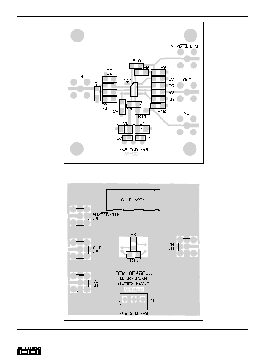
BOARD LAYOUT
This demonstration board is a two layer PCB. It uses a
ground plane on the bottom and signal and power traces on
the top. The ground plane has been opened up around op
amp pins sensitive to capacitive loading. Power supply
traces are laid out to keep current loop areas to a minimum.
The SMA (or SMB) connectors may be mounted either
vertically or horizontally.
The location and type of capacitors used for power-supply
bypassing are crucial to high frequency amplifiers. The
tantalum capacitors, C
1
and C
2
, do not need to be as close to
pins 7 and 4 on your PCB, and may be shared with other
amplifiers.
See the individual op amp data sheet for more information
on proper board layout techniques, and component selec-
tion.
MEASUREMENT TIPS
This demonstration board and the component values shown
are designed to operate in a 50
environment. Most data
sheet plots are obtained this way. Change the component
values for different input and output impedance levels.
Do not use high impedance probes; they represent a heavy
capacitive load to the op amps, and will alter their response.
Instead, use low impedance (
500
) probes with adequate
bandwidth. The probe input capacitance and resistance set
an upper limit on the measurement bandwidth. If a high
impedance probe must be used, place a 100
resistor on the
probe tip to isolate its capacitance from the circuit.
4
Æ
DEM-OPA68xU
FIGURE 3. DEM-OPA68xU Demonstration Board Layout; (a) Component Side Silkscreen and Metal, (b) Ground Plane Side
Silkscreen and Metal (bottom view).
(a)
(b)