 | ÐлекÑÑоннÑй компоненÑ: OPA685U | СкаÑаÑÑ:  PDF PDF  ZIP ZIP |
Äîêóìåíòàöèÿ è îïèñàíèÿ www.docs.chipfind.ru
Ultra-Wideband, Current-Feedback
OPERATIONAL AMPLIFIER With Disable
TM
DESCRIPTION
The OPA685 is a very high bandwidth, current-feed-
back op amp that combines exceptional 4200V/
µ
s slew
rate and low input voltage noise to deliver a precision
low cost, high dynamic range Intermediate Frequency
(IF) amplifier. Optimized for high gain operation, the
OPA685 is ideally suited to buffering Surface Acoustic
Wave (SAW) filters in an IF strip or delivering high
output power at low distortion for cable modem up-
stream line drivers. Even higher bandwidth at lower
gains gives a 900MHz video line driver for high
resolution workstation graphics.
The OPA685's low 12.9mA supply current is pre-
cisely trimmed at +25
°
C. This trim, along with a low
temperature drift, guarantees low system power over-
OPA685
®
FEATURES
q
GAIN = +2 BANDWIDTH (900MHz)
q
GAIN = +8 BANDWIDTH (420MHz)
q
OUTPUT VOLTAGE SWING:
±
3.6V
q
ULTRA-HIGH SLEW RATE: 4200V/
µ
s
q
3RD-ORDER INTERCEPT: > 40dBm (f < 50MHz)
q
LOW POWER: 129mW
q
LOW DISABLED POWER: 3mW
APPLICATIONS
q
LOW COST PRECISION IF AMPLIFIER
q
CABLE MODEM UPSTREAM DRIVER
q
BROADBAND VIDEO LINE DRIVER
q
VERY WIDEBAND ADC BUFFER
q
PORTABLE INSTRUMENTS
q
ACTIVE FILTERS
q
ARB WAVEFORM OUTPUT DRIVER
OPA685 RELATED PRODUCTS
SINGLES
DUALS
OPA658
OPA2658
OPA681
OPA2681
OPA682
OPA2682
©
1999 Burr-Brown Corporation
PDS-1499A
Printed in U.S.A. April, 1999
International Airport Industrial Park · Mailing Address: PO Box 11400, Tucson, AZ 85734 · Street Address: 6730 S. Tucson Blvd., Tucson, AZ 85706 · Tel: (520) 746-1111
Twx: 910-952-1111 · Internet: http://www.burr-brown.com/ · Cable: BBRCORP · Telex: 066-6491 · FAX: (520) 889-1510 · Immediate Product Info: (800) 548-6132
temperature. System power may be further reduced
using the optional disable control pin. Leaving this pin
open, or holding it HIGH, gives normal operation. If
pulled LOW, the OPA685 supply current drops to less
than 320
µ
A. This power-savings feature, along with
exceptional single +5V operation, and ultra-small
SOT23-6 packaging, make the OPA685 ideal for por-
table communications requirements.
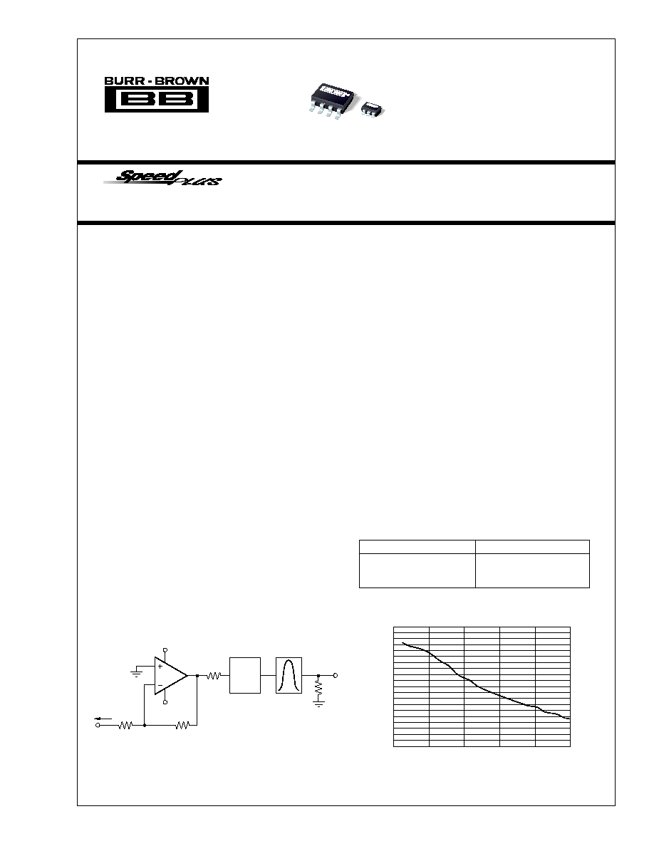
Low Distortion, 12dB Gain SAW Driver
OPA685
OPA685
For most current data sheet and other product
information, visit www.burr-brown.com
OPA685
SAW
Filter
+5V
5V
Matching
Network
50
Source
50
50
400
50
50
40
30
20
10
Center Frequency (MHz)
0
50
150
250
200
100
TWO-TONE, 3rd-ORDER
INTERMODULATION INTERCEPT
Output Intercept (dBm)
2
®
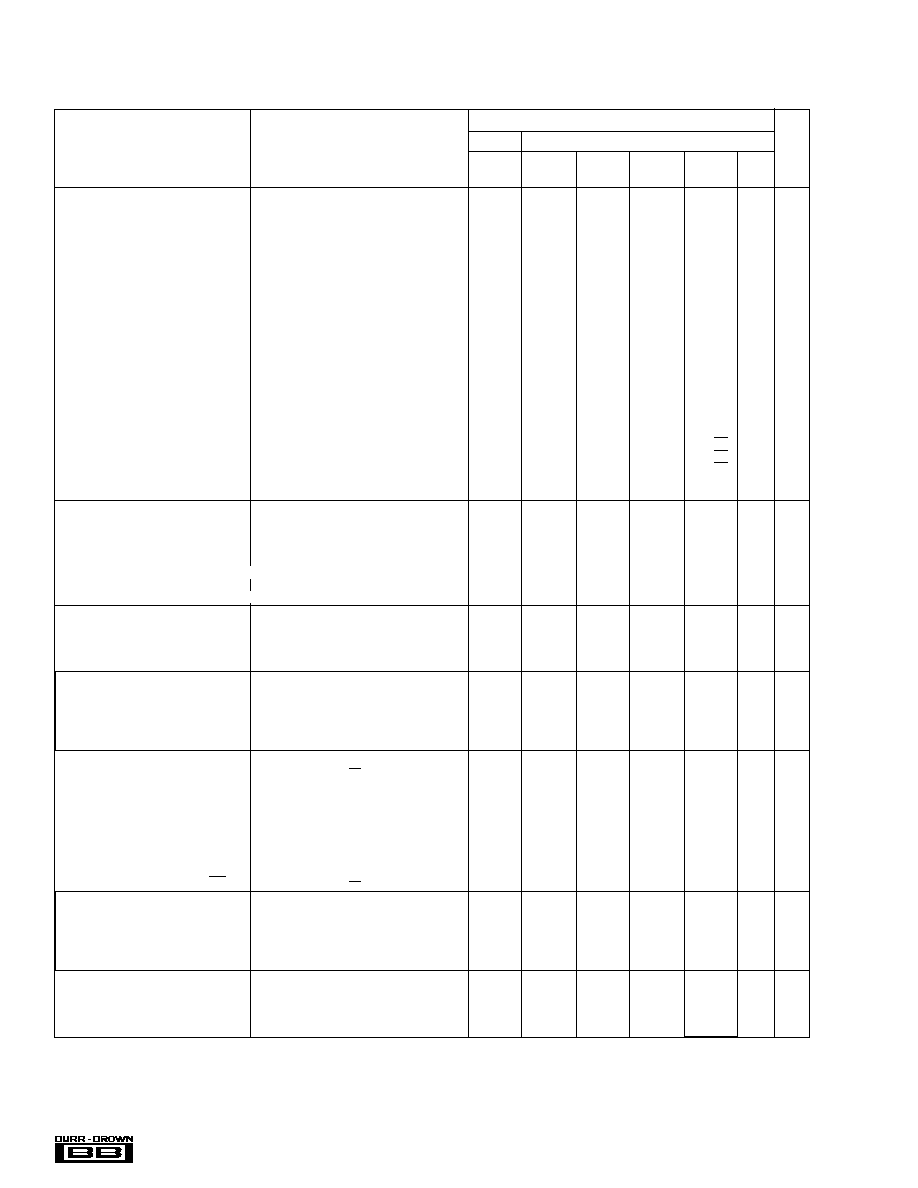
OPA685
SPECIFICATIONS: V
S
=
±
5V
R
F
= 402
, R
L
= 100
, and G = +8
,
(Figure 1 for AC performance only), unless otherwise noted.
OPA685U, N
TYP
GUARANTEED
0
°
C to
40
°
C to
MIN/
TEST
PARAMETER
CONDITIONS
+25
°
C
+25
°
C
(2)
70
°
C
(3)
+85
°
C
(3)
UNITS
MAX
LEVEL
(1)
AC PERFORMANCE (Figure 1)
Small-Signal Bandwidth (V
O
= 0.5Vp-p)
G = +1, R
F
= 523
1200
MHz
typ
C
G = +2, R
F
= 511
900
MHz
typ
C
G = +8, R
F
= 402
420
360
350
320
MHz
min
B
G = +16, R
F
= 249
340
MHz
typ
C
Bandwidth for 0.1dB Gain Flatness
G = +2, V
O
= 0.5Vp-p, R
F
=523
350
150
80
70
MHz
min
B
Peaking at a Gain of +1
R
F
= 523
, V
O
= 0.5Vp-p
3
4.5
5
6.0
dB
max
B
Large Signal Bandwidth
G = +8, V
O
= 4Vp-p
350
MHz
typ
C
Slew Rate
G = 8, V
O
= 4V Step
4200
3000
2500
2200
V/
µ
s
min
B
G = +8, V
O
= 4V Step
2900
2400
2400
2100
V/
µ
s
min
B
Rise/Fall Time
G = +8, V
O
= 0.5V Step
0.7
ns
typ
C
G = +8, V
O
= 4V Step
1.0
ns
typ
C
Settling Time to 0.02%
G = +8, V
O
= 2V Step
4
ns
typ
C
0.1%
G = +8, V
O
= 2V Step
3
ns
typ
C
Harmonic Distortion
G = +8, f = 10MHz, V
O
= 2Vp-p
2nd Harmonic
R
L
= 100
66
59
56
53
dBc
max
B
R
L
500
75
69
66
63
dBc
max
B
3rd Harmonic
R
L
= 100
90
83
77
74
dBc
max
B
R
L
500
84
78
76
75
dBc
max
B
Input Voltage Noise
f > 1MHz
1.7
1.8
2.2
2.3
nV/
Hz
max
B
Non-Inverting Input Current Noise
f > 1MHz
13
15
15
15
pA/
Hz
max
B
Inverting Input Current Noise
f > 1MHz
19
22
22
22
pA/
Hz
max
B
Differential Gain
G = +2, NTSC, V
O
= 1.4Vp, R
L
= 150
0.10
%
typ
C
Differential Phase
G = +2, NTSC, V
O
= 1.4Vp, R
L
= 150
0.01
deg
typ
C
DC PERFORMANCE
(4)
Open-Loop Transimpedance Gain (Z
OL
)
V
O
= 0V, R
L
= 100
42
26
24
23
k
min
A
Input Offset Voltage
V
CM
= 0V
±
1.7
±
3.5
±
5
±
7
mV
max
A
Average Offset Voltage Drift
V
CM
= 0V
+35
+40
µ
V/
°
C
max
B
Non-Inverting Input Bias Current
V
CM
= 0V
+56
+90
±
100
±
130
µ
A
max
A
Average Non-Inverting Input Bias Current Drift
V
CM
= 0V
530
570
nA/
°
C
max
B
Inverting Input Bias Current
V
CM
= 0V
±
10
±
100
±
120
±
150
µ
A
max
A
Average Inverting Input Bias Current Drift
V
CM
= 0V
500
560
nA
°
/C
max
B
INPUT
Common-Mode Input Range
(5)
(CMIR)
±
3.4
±
3.2
±
3.1
±
3.0
V
min
A
Common-Mode Rejection Ratio (CMRR)
V
CM
= 0V
54
49
48
48
dB
min
A
Non-Inverting Input Impedance
87 || 2
k
|| pF
typ
C
Inverting Input Resistance (R
I
)
Open-Loop
19
typ
C
OUTPUT
Voltage Output Swing
No Load
±
4.1
±
3.9
±
3.8
±
3.8
V
min
A
100
Load
±
3.6
±
3.3
±
3.2
±
3.1
V
min
A
Current Output, Sourcing
V
O
= 0
+130
+90
+75
+70
mA
min
A
Current Output, Sinking
V
O
= 0
90
60
50
45
mA
min
A
Closed-Loop Output Impedance
G = +8, f = 100kHz
0.2
typ
C
DISABLE (Disabled Low)
Power Down Supply Current (+V
S
)
V
DIS
= 0
320
µ
A
typ
C
Disable Time
100
ns
typ
C
Enable Time
100
ns
typ
C
Off Isolation
G = +8, 10MHz
70
dB
typ
C
Output Capacitance in Disable
3
pF
typ
C
Turn On Glitch
G = +2, R
L
= 150
, V
IN
= 0
±
160
mV
typ
C
Turn Off Glitch
G = +2, R
L
= 150
, V
IN
= 0
±
20
mV
typ
C
Enable Voltage
3.3
3.5
3.6
3.7
V
min
A
Disable Voltage
1.8
1.7
1.6
1.5
V
max
A
Control Pin Input Bias Current (DIS)
V
DIS
= 0
115
160
160
160
µ
A
max
A
POWER SUPPLY
Specified Operating Voltage
±
5
V
typ
C
Maximum Operating Voltage Range
±
6
±
6
±
6
V
max
A
Max Quiescent Current
V
S
=
±
5V
12.9
13.5
13.5
13.5
mA
max
A
Min Quiescent Current
V
S
=
±
5V
12.9
12.5
11.9
11.2
mA
min
A
Power Supply Rejection Ratio (PSRR)
Input Referred
55
49
47
46
dB
typ
A
TEMPERATURE RANGE
Specification: U, N
40 to +85
°
C
typ
C
Thermal Resistance,
JA
Junction-to-Ambient
U
SO-8
125
°
C/W
typ
C
N
SOT23-6
150
°
C/W
typ
C
NOTES: (1) Test levels: (A) 100% tested at 25
°
C. Over temperature limits by characterization and simulation. (B) Limits set by characterization and simulation.
(C) Typical value only for information. (2) Junction temperature = ambient for 25
°
C guaranteed specifications. (3) Junction temperature = ambient at low temperature
limit: junction temperature = ambient +23
°
C at high temperature limit for over temperature guaranteed specifications. (4) Current is considered positive out-of-node.
V
CM
is the input common-mode voltage. (5) Tested < 3dB below minimum specified CMRR at
±
CMIR limits.
3
®
OPA685
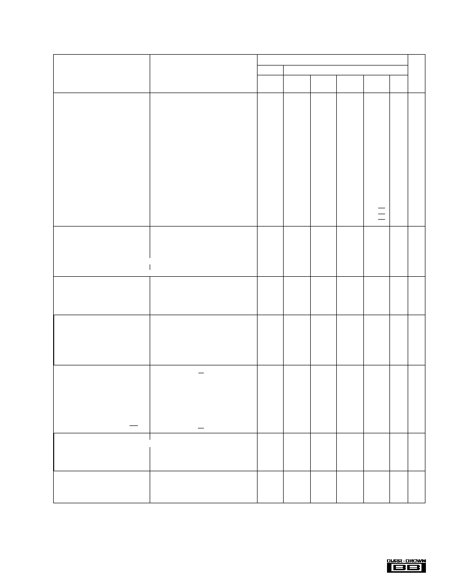
SPECIFICATIONS: V
S
= +5V
R
F
= 348
, R
L
= 100
to V
S
/2, and G = +8
,
(Figure 3 for AC performance only), unless otherwise noted.
OPA685U, N
TYP
GUARANTEED
0
°
C to
40
°
C to
MIN/
TEST
PARAMETER
CONDITIONS
+25
°
C
+25
°
C
(2)
70
°
C
(3)
+85
°
C
(3)
UNITS
MAX
LEVEL
(1)
AC PERFORMANCE (Figure 3)
Small-Signal Bandwidth (V
O
= 0.5Vp-p)
G = +1, R
F
= 511
600
MHz
typ
C
G = +2, R
F
= 487
450
MHz
min
B
G = +8, R
F
= 348
350
240
220
200
MHz
typ
C
G = +16, R
F
= 162
250
MHz
typ
C
Bandwidth for 0.1dB Gain Flatness
G = +2, V
O
< 0.5Vp-p, R
F
= 487
140
80
70
60
MHz
min
B
Peaking at a Gain of +1
R
F
= 511
, V
O
< 0.5Vp-p
0.4
1.0
1.5
1.5
dB
max
B
Large Signal Bandwidth
G = +8, V
O
= 2Vp-p
350
MHz
typ
C
Slew Rate
G = +8, 2V Step
1900
1300
1200
1100
V/
µ
s
min
B
Rise/Fall Time
G = +8, V
O
= 0.5V Step
0.8
ns
typ
C
G = +8, V
O
= 2V Step
1.0
ns
typ
C
Settling Time to 0.02%
G = +8, V
O
= 2V Step
9
ns
typ
C
0.1%
G = +8, V
O
= 2V Step
7
ns
typ
C
Harmonic Distortion
G = +8, f = 10MHz, V
O
= 2Vp-p
2nd Harmonic
R
L
= 100
to V
S
/ 2
60
54
53
52
dBc
max
B
R
L
500
to V
S
/2
68
60
59
58
dBc
max
B
3rd Harmonic
R
L
= 100
to V
S
/ 2
58
51
50
50
dBc
max
B
R
L
500
to V
S
/2
60
55
54
54
dBc
max
B
Input Voltage Noise
f > 1MHz
1.7
1.8
2.2
2.2
nV/
Hz
max
B
Non-Inverting Input Current Noise
f > 1MHz
13
15
15
15
pA/
Hz
max
B
Inverting Input Current Noise
f > 1MHz
19
22
22
22
pA/
Hz
max
B
DC PERFORMANCE
(4)
Open-Loop Transimpedance Gain (Z
OL
)
V
O
= V
S
/2, R
L
= 100
to V
S
/2
40
25
23
20
k
min
A
Input Offset Voltage
V
CM
= V
S
/2
±
1
±
3
±
3.5
±
4.0
mV
max
A
Average Offset Voltage Drift
V
CM
= V
S
/2
12
15
µ
V/
°
C
max
B
Non-Inverting Input Bias Current
V
CM
= V
S
/2
+40
+110
±
120
±
150
µ
A
max
A
Average Non-Inverting Input Bias Current Drift
V
CM
= V
S
/2
550
650
nA/
°
C
max
B
Inverting Input Bias Current
V
CM
= V
S
/2
±
50
±
100
±
120
±
150
µ
A
max
A
Average Inverting Input Bias Current Drift
V
CM
= V
S
/2
550
650
nA /
°
C
max
B
INPUT
Least Positive Input Voltage
(5)
1.7
1.8
1.9
2.0
V
max
A
Most Positive Input Voltage
(5)
3.3
3.2
3.1
3.0
V
min
A
Common-Mode Rejection Ratio (CMRR)
V
CM
= V
S
/2
54
48
47
47
dB
min
A
Non-Inverting Input Impedance
87 || 2
k
|| pF
typ
C
Inverting Input Resistance (R
I
)
Open-Loop
23
typ
C
OUTPUT
Most Positive Output Voltage
No Load
4.1
3.9
3.7
3.5
V
min
A
R
L
= 100
to V
S
/2
4.0
3.8
3.6
3.4
V
min
A
Least Positive Output Voltage
No Load
0.9
1.1
1.3
1.5
V
max
A
R
L
= 100
to V
S
/2
1.0
1.2
1.4
1.6
V
max
A
Current Output, Sourcing
V
O
= V
S
/2
90
62
60
58
mA
min
A
Current Output, Sinking
V
O
= V
S
/2
70
45
40
38
mA
min
A
Closed-Loop Output Impedance
G = +2, f = 100kHz
0.3
typ
C
DISABLE (Disable Low)
Power Down Supply Current (+V
S
)
V
DIS
= 0
270
µ
A
typ
C
Disable Time
150
ns
typ
C
Enable Time
150
ns
typ
C
Off Isolation
G = +8, 10MHz
70
dB
typ
C
Output Capacitance in Disable
3
pF
typ
C
Turn On Glitch
G = +2, R
L
= 150
, V
IN
= V
S
/2
±
160
mV
typ
C
Turn Off Glitch
G = +2, R
L
= 150
, V
IN
= V
S
/2
±
20
mV
typ
C
Enable Voltage
3.3
3.5
3.6
3.7
V
min
A
Disable Voltage
1.8
1.7
1.6
1.5
V
max
A
Control Pin Input Bias Current (DIS)
V
DIS
= 0
100
µ
A
typ
C
POWER SUPPLY
Specified Single-Supply Operating Voltage
5
V
typ
C
Max Single-Supply Operating Voltage
12
12
12
V
max
A
Max Quiescent Current
V
S
= +5V
10.7
11.3
11.3
11.3
mA
max
A
Min Quiescent Current
V
S
= +5V
10.7
9.0
8.3
8.1
mA
min
A
Power Supply Rejection Ratio (PSRR)
Input Referred
54
51
49
48
dB
min
A
TEMPERATURE RANGE
Specification: U, N
40 to +85
°
C
typ
C
Thermal Resistance,
JA
Junction-to-Ambient
U
SO-8
125
°
C/W
typ
C
N
SOT23-6
150
°
C/W
typ
C
NOTES: (1) Test levels: (A) 100% tested at 25
°
C. Over temperature limits by characterization and simulation. (B) Limits set by characterization and simulation.
(C) Typical value only for information. (2) Junction temperature = ambient for 25
°
C guaranteed specifications. (3) Junction temperature = ambient at low temperature
limit: junction temperature = ambient +23
°
C at high temperature limit for over temperature guaranteed specifications. (4) Current is considered positive out-of-node.
V
CM
is the input common-mode voltage. (5) Tested < 3dB below minimum specified CMRR at
±
CMIR limits.

4
®
OPA685
ABSOLUTE MAXIMUM RATINGS
Power Supply ..............................................................................
±
6.5VDC
Internal Power Dissipation ................................ See Thermal Information
Differential Input Voltage ..................................................................
±
1.2V
Input Voltage Range ............................................................................
±
V
S
Storage Temperature Range: U, N ................................ 40
°
C to +125
°
C
Lead Temperature (soldering, 10s) .............................................. +300
°
C
Junction Temperature (T
J
) ........................................................... +175
°
C
The information provided herein is believed to be reliable; however, BURR-BROWN assumes no responsibility for inaccuracies or omissions. BURR-BROWN assumes
no responsibility for the use of this information, and all use of such information shall be entirely at the user's own risk. Prices and specifications are subject to change
without notice. No patent rights or licenses to any of the circuits described herein are implied or granted to any third party. BURR-BROWN does not authorize or warrant
any BURR-BROWN product for use in life support devices and/or systems.
PACKAGE
SPECIFIED
DRAWING
TEMPERATURE
PACKAGE
ORDERING
TRANSPORT
PRODUCT
PACKAGE
NUMBER
(1)
RANGE
MARKING
NUMBER
MEDIA
OPA685U
SO-8 Surface Mount
182
40
°
C to +85
°
C
OPA685U
OPA685U
Rails
"
"
"
"
"
OPA685U/2K5
Tape and Reel
OPA685N
SOT23-6
332
40
°
C to +85
°
C
A85
OPA685N/250
Tape and Reel
"
"
"
"
"
OPA685N/3K
Tape and Reel
NOTES: (1) For detailed drawing and dimension table, please see end of data sheet, or Appendix C of Burr-Brown IC Data Book. (2) Models with a slash (/) are available
only as Tape and Reel in the quantity indicated after the slash (e.g. /3K indicates 3000 devices per reel). Ordering 3000 pieces of the OPA685N/3K will get a single
3000-piece Tape and Reel. For detailed Tape and Reel mechanical information, refer to Appendix B of the Burr-Brown IC Data Book.
PACKAGE/ORDERING INFORMATION
ELECTROSTATIC
DISCHARGE SENSITIVITY
Electrostatic discharge can cause damage ranging from perfor-
mance degradation to complete device failure. Burr-Brown Corpo-
ration recommends that all integrated circuits be handled and stored
using appropriate ESD protection methods.
ESD damage can range from subtle performance degradation to
complete device failure. Precision integrated circuits may be more
susceptible to damage because very small parametric changes
could cause the device not to meet published specifications.
PIN CONFIGURATIONS
Top View
SO-8
NC = No Connection
Top View
SOT23-6
1
2
3
4
8
7
6
5
NC
Inverting Input
Non-Inverting Input
V
S
DIS
+V
S
Output
NC
1
2
3
6
5
4
Output
V
S
Non-Inverting Input
+V
S
DIS
Inverting Input
1
2
3
6
5
4
A85
Pin Orientation/Package Marking
5
®
OPA685
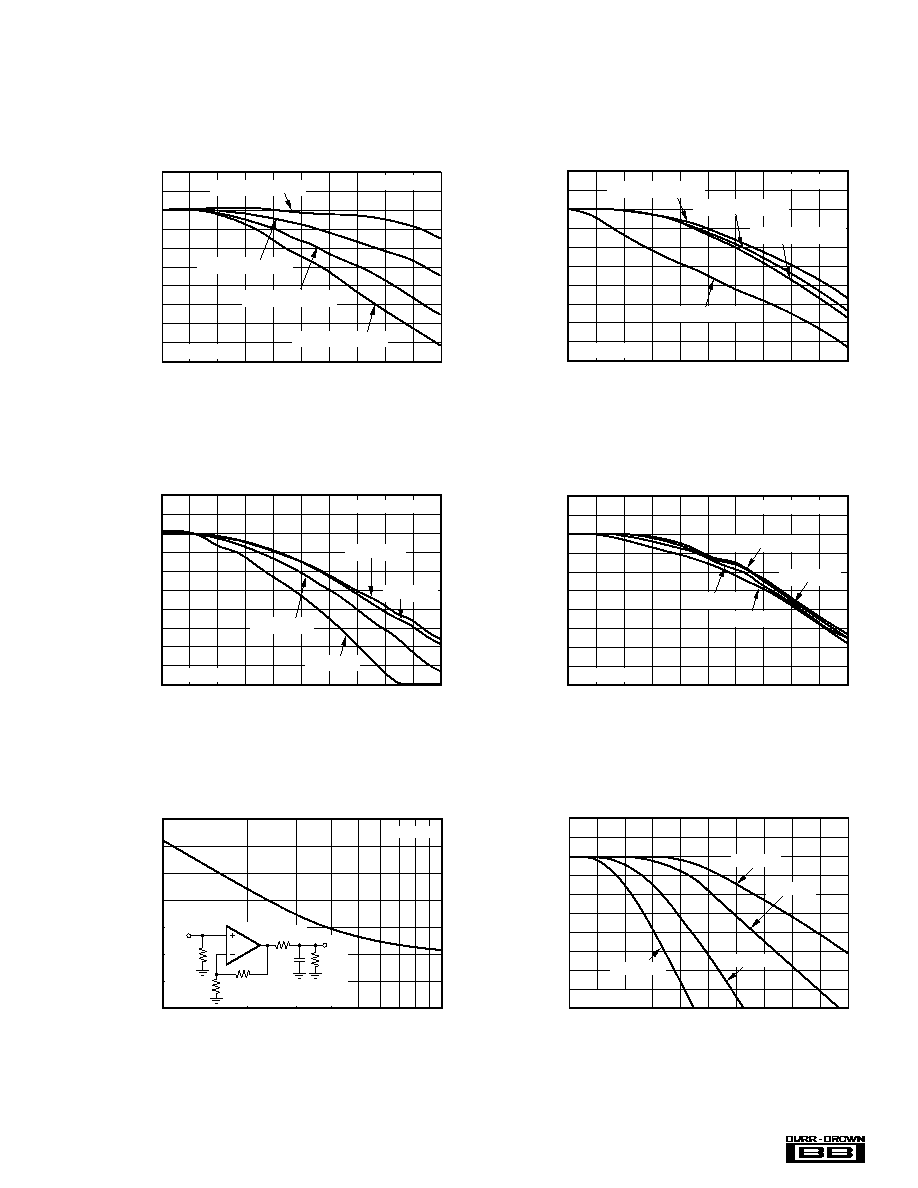
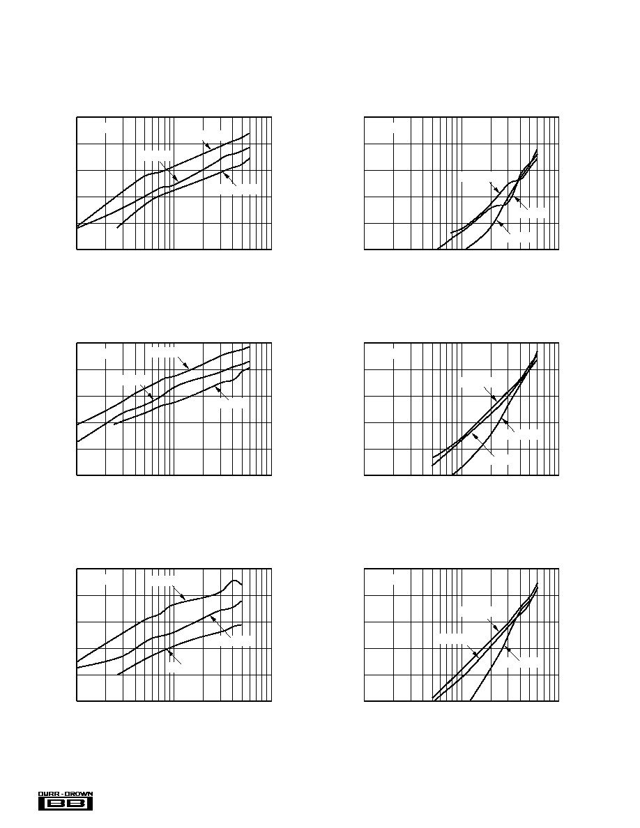
TYPICAL PERFORMANCE CURVES: V
S
=
±
5V
G = +8, R
F
= 402
, and R
L
= 100
, unless otherwise noted.
6
3
0
3
6
9
12
15
18
21
24
Frequency (100MHz/div)
0
1GHz
500MHz
NON-INVERTING SMALL-SIGNAL
FREQUENCY RESPONSE
Normalized Gain (3dB/div)
G = +16, R
F
= 249
G = +8, R
F
= 402
See Figure 1
G = +2, R
F
= 511
V
O
= 500mVp-p
G = +4, R
F
= 475
24
21
18
15
12
9
6
3
0
3
6
Frequency (100MHz/div)
0
1GHz
500MHz
INVERTING LARGE-SIGNAL
FREQUENCY RESPONSE
Gain (3dB/div)
V
O
= 4Vp-p
V
O
= 7Vp-p
G = 8, R
F
= 442
V
O
= 1Vp-p
V
O
= 2Vp-p
See Figure 2
70
60
50
40
30
20
10
0
10
100
G = +8
OPA685
R
S
V
I
C
L
V
O
402
56.2
1k
is optional
50
1k
RECOMMENDED R
S
vs CAPACITIVE LOAD
Capacitive Load (pF)
R
S
(
)
21
18
15
12
9
6
3
0
3
0
250 MHz
500 MHz
Frequency (50MHz/div)
Gain-to-Capacitive Load (3dB/div)
FREQUENCY RESPONSE vs CAPACITIVE LOAD
C
L
= 10pF
C
L
= 20pF
C
L
= 47pF
C
L
= 100pF
Optimized R
S
24
21
18
15
12
9
6
3
0
3
6
Frequency (100MHz/div)
0
1GHz
500MHz
NON-INVERTING LARGE-SIGNAL
FREQUENCY RESPONSE
Gain (3dB/div)
V
O
= 7Vp-p
V
O
= 2Vp-p
V
O
= 4Vp-p
G = +8, R
F
= 402
See Figure 1
V
O
= 1Vp-p
6
3
0
3
6
9
12
15
18
21
23
Frequency (100MHz/div)
0
1GHz
500MHz
INVERTING SMALL-SIGNAL
FREQUENCY RESPONSE
Normalized Gain (3dB/div)
G = 16, R
F
= 806
G = 2, R
F
= 499
V
O
= 500mVp-p
G = 2, R
F
= 499
G = 4, R
F
= 475
G = 8, R
F
= 442
See Figure 2
6
®
OPA685
TYPICAL PERFORMANCE CURVES: V
S
=
±
5V
(CONT)
G = +8, R
F
= 402
, and R
L
= 100
, unless otherwise noted. See Figure 1.
50
60
70
80
90
100
10MHz 2nd HARMONIC DISTORTION
vs OUTPUT VOLTAGE
Output Voltage (Vp-p)
0.1
1
10
2nd Harmonic Distortion (dBc)
R
L
= 500
R
L
= 100
R
L
= 200
G = +8V/V
50
60
70
80
90
100
10MHz 3rd HARMONIC DISTORTION
vs OUTPUT VOLTAGE
Output Voltage (Vp-p)
0.1
1
10
3rd Harmonic Distortion (dBc)
R
L
= 500
R
L
= 100
R
L
= 200
G = +8V/V
50
60
70
80
90
100
20MHz 2nd HARMONIC DISTORTION
vs OUTPUT VOLTAGE
Output Voltage (Vp-p)
0.1
1
10
2nd Harmonic Distortion (dBc)
R
L
= 500
R
L
= 200
G = +8V/V
R
L
= 100
50
60
70
80
90
100
20MHz 3rd HARMONIC DISTORTION
vs OUTPUT VOLTAGE
Output Voltage (Vp-p)
0.1
1
10
3rd Harmonic Distortion (dBc)
R
L
= 500
R
L
= 100
R
L
= 200
G = +8V/V
40
50
60
70
80
90
50MHz 2nd HARMONIC DISTORTION
vs OUTPUT VOLTAGE
Output Voltage (Vp-p)
0.1
1
10
2nd Harmonic Distortion (dBc)
R
L
= 500
R
L
= 200
R
L
= 100
G = +8V/V
40
50
60
70
80
90
50MHz 3rd HARMONIC DISTORTION
vs OUTPUT VOLTAGE
Output Voltage (Vp-p)
0.1
1
10
3rd Harmonic Distortion (dBc)
R
L
= 100
R
L
= 200
G = +8V/V
R
L
= 500
7
®
OPA685
TYPICAL PERFORMANCE CURVES: V
S
=
±
5V
(CONT)
G = +8, R
F
= 402
, and R
L
= 100
, unless otherwise noted. See Figure 1.
40
50
60
70
80
90
2nd HARMONIC DISTORTION
vs FREQUENCY
Frequency (MHz)
1
10
100
2nd Harmonic Distortion (dBc)
G = +2,
R
F
= 511
G = +4,
R
F
= 475
G = +8
R
F
= 402
G = +16
R
F
= 249
V
O
= 2Vp-p
R
L
= 100
40
50
60
70
80
90
3rd HARMONIC DISTORTION
vs FREQUENCY
Frequency (MHz)
1
10
100
3rd Harmonic Distortion (dBc)
G = +4
R
F
= 475
G = +16
R
F
= 249
V
O
= 2Vp-p
R
L
= 100
G = +8
R
F
= 402
G = +2
R
F
= 511
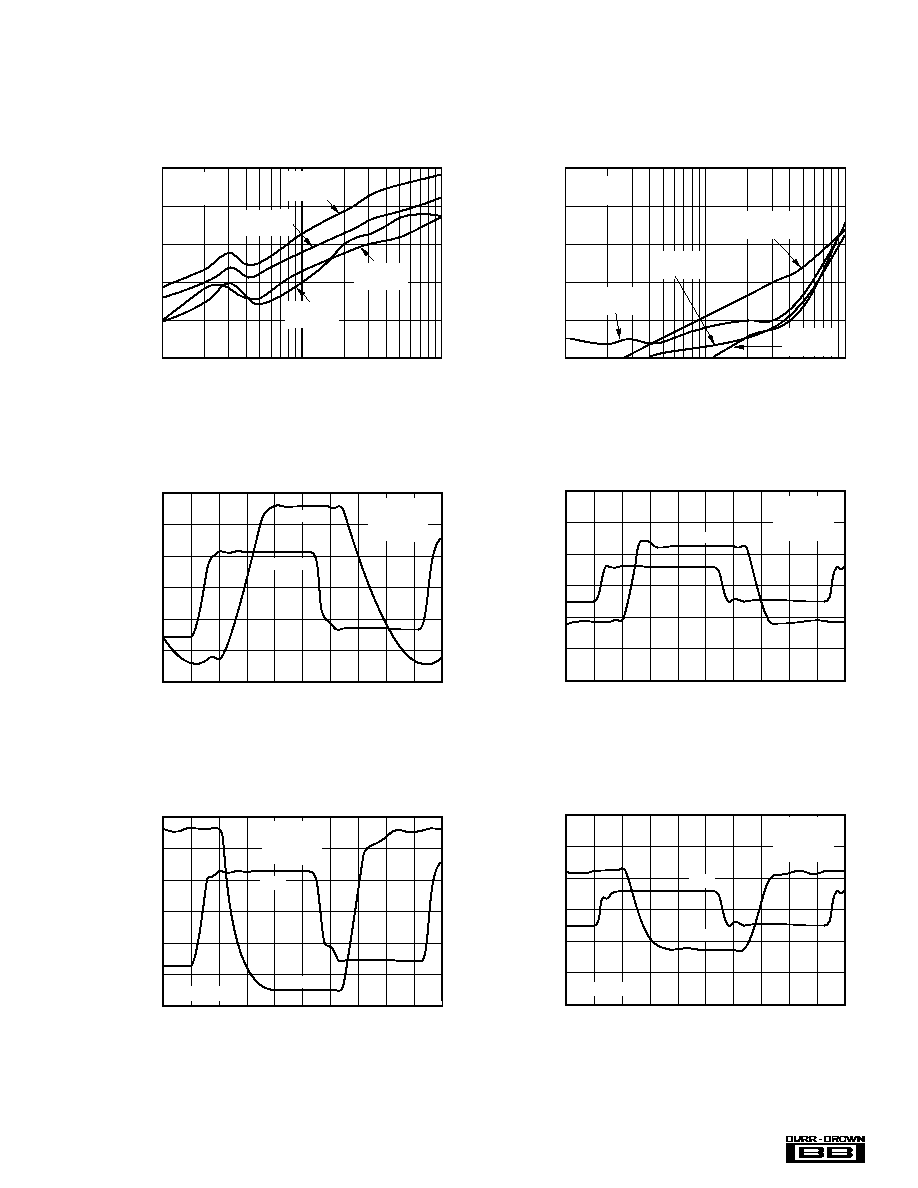
NON-INVERTING LARGE-SIGNAL PULSE RESPONSE
Time (1ns/div)
800mV/div
G = +2
R
F
= 511
V
O
= 4Vp-p
Output
Input
2400
1600
800
0
800
1600
2400
NON-INVERTING SMALL-SIGNAL PULSE RESPONSE
Time (1ns/div)
400mV/div
1200
800
400
0
400
800
1200
Output
Input
G = +2
R
F
= 511
V
O
= 1Vp-p
INVERTING LARGE-SIGNAL PULSE RESPONSE
Time (1ns/div)
800mV/div
Input
2400
1600
800
0
800
1600
2400
Output
See Figure 2
G = 8
R
F
= 442
V
O
= 4Vp-p
INVERTING SMALL-SIGNAL PULSE RESPONSE
Time (1ns/div)
400mV/div
1200
800
400
0
400
800
1200
G = 8
R
F
= 442
V
O
= 1Vp-p
Output
Input
See Figure 2
8
®
OPA685
TYPICAL PERFORMANCE CURVES: V
S
=
±
5V
(CONT)
G = +8, R
F
= 402
, and R
L
= 100
, unless otherwise noted.
15
20
25
30
35
40
45
50
55
60
65
ISOLATION CHARACTERISTICS vs FREQUENCY
Frequency (Hz)
10M
100M
1G
Isolation (dB)
G = 8 (see Figure 2)
Reverse Isolation (S
12
)
G = +8 (see Figure 1)
Disabled Isolation (S
21
)
G = +8 (see Figure 1)
Reverse Isolation (S
12
)
20
15
10
5
Gain to Matched Load (dB)
6
12
8
9.5
11
NOISE FIGURE vs GAIN
Noise Figure (dB)
Non-Inverting Gain with
50
Input Match
Non-Inverting Gain with
1:2 Input Transformer
(see Figure 5)
See Tables I, II, III
R
S
= 50
T
A
= +25
°
C
Optimized R
F
Inverting Gain with
50
Input Match
100
10
1
INPUT VOLTAGE AND CURRENT NOISE DENSITY
Frequency (Hz)
100
1k
10k
100k
1M
10M
Current Noise (pA/
Hz)
Voltage Noise (nV/
Hz)
Non-Inverting Input Current Noise
Inverting Input Current Noise
13pA/
Hz
19pA/
Hz
Input Voltage Noise
1.7nV/
Hz
5
10
15
20
25
30
35
40
45
50
55
INPUT RETURN LOSS vs FREQUENCY (S
11
)
Frequency (Hz)
10M
100M
1G
Return Loss (5dB/div)
G = +8
(see Figure 1)
G = 8
(see Figure 2)
VSWR < 1.2:1
5
10
15
20
25
30
35
40
45
50
55
OUTPUT RETURN LOSS vs FREQUENCY (S
22
)
Frequency (Hz)
10M
100M
1G
Return Loss (5dB/div)
G =
±
8
Without
Trim Cap
With
Trim Cap
VSWR < 1.2:1
OPA685
50
3.3pF
S
22
Trim Cap
50
40
30
20
10
Center Frequency (MHz)
0
50
150
250
200
100
TWO-TONE, 3rd-ORDER
INTERMODULATION INTERCEPT
Output Intercept (dBm)
OPA685
P
I
P
O
402
50
50
50
56.2
G = 12dB to matched load.
OPA685
P
I
P
O
402
50
50
50
G = 12dB to matched load.
G = +8
G = 8
9
®
OPA685
TYPICAL PERFORMANCE CURVES: V
S
=
±
5V
(CONT)
G = +8, R
F
= 402
, and R
L
= 100
, unless otherwise noted.
0.2
0.18
0.16
0.14
0.12
0.1
0.08
0.06
0.04
0.02
0.
Number of Video Loads
1
2
3
4
COMPOSITE VIDEO dG/d
dG/d
(%/
°
)
dG, Positive Video
d
, Negative Video
d
, Positive Video
dG, Negative Video
G = +2
R
F
= 511
6.1
6.0
5.9
+1.0
+0.5
0
0.5
1.0
0
100
200
Frequency (20MHz/div)
Gain (0.1dB/div)
Phase (0.5
°
/div)
GAIN FLATNESS AND DEVIATION FROM
LINEAR PHASE vs FREQUENCY
Deviation from Linear Phase
Right Scale
Gain
Left Scale
G = +2
R
L
= 100
R
F
= 523
60
55
50
45
40
35
30
25
20
10
2
10
3
10
4
10
5
10
6
10
7
10
8
CMRR AND PSRR vs FREQUENCY
Frequency (Hz)
Rejection Ratio (dB)
+PSRR
PSRR
CMRR
95
85
75
65
55
45
35
OPEN-LOOP TRANSIMPEDANCE GAIN/PHASE
Frequency (Hz)
100k
1M
10M
100M
1G
10G
Log Transimpedance Gain (10dB
/div)
0
40
80
120
160
200
240
Open-Loop Phase (40
°
/div)
| Z
OL
|
Z
OL
15
12
9
6
3
0
150
120
90
60
30
0
40
10
20
50
80
110
140
SUPPLY AND OUTPUT CURRENT vs TEMPERATURE
Temperature (C)
Supply Current (mA)
Output Current (mA)
Supply Current
Sourcing Output Current
Sinking Output Current
5
4
3
2
1
0
1
2
3
4
5
100
80
60
40
20
0
20
40
60
80
100
40
20
0
20
40
60
80
100
120
140
TYPICAL DC DRIFT OVER TEMPERATURE
Ambient Temperature (
°
C)
Input Of
fset V
oltage (mV)
Input Bias Current (
µ
A)
Inverting Input
Bias Current
Non-Inverting Input
Bias Current
V
IO
10
®
OPA685
TYPICAL PERFORMANCE CURVES: V
S
=
±
5V
(CONT)
G = +8, R
F
= 402
, and R
L
= 100
, unless otherwise noted.
OUTPUT VOLTAGE AND CURRENT LIMITATIONS
5
4
3
2
1
0
1
2
3
4
5
I
O
(mA)
100
80
40
20
60
0
20
40
60
80
100
V
O
(Volts)
100
Load Line
Output Current Limit
Output Current Limit
200
Load Line
500
Load Line
10
1
0.1
10k
100k
1M
10M
100M
CLOSED-LOOP OUTPUT IMPEDANCE
Frequency (Hz)
Output Impedance (
)
OPA685
402
56.2
50
Z
O
11
®
OPA685
TYPICAL PERFORMANCE CURVES: V
S
= +5V
G = +8, R
F
= 348
, and R
L
= 100
, unless otherwise noted.
70
60
50
40
30
20
10
0
RECOMMENDED R
S
vs CAPACITIVE LOAD
Capacitive Load (pF)
10
100
R
S
(
)
OPA685
348
35.7
52.3
2.5k
2.5k
1k
V
I
+5V
0.1
µ
F
1k
load is optional
V
O
R
S
C
L
0.1
µ
F
24
21
18
15
12
9
6
3
0
3
6
Frequency (50MHz/div)
0
500MHz
250MHz
FREQUENCY RESPONSE vs CAPACITIVE LOAD
Gain-to-Capacitive Load (3dB/div)
C
L
= 10pF
C
L
= 100pF
Optimized R
S
C
L
= 20pF
C
L
= 47pF
6
3
0
3
6
9
12
15
18
21
24
Frequency (100MHz/div)
0
1GHz
500MHz
NON-INVERTING SMALL-SIGNAL
FREQUENCY RESPONSE
Normalized Gain (3dB/div)
G = +8, R
F
= 348
G = +4, R
F
= 442
G = +16, R
F
= 162
See Figure 3
G = +2, R
F
= 487
V
O
= 500mVp-p
NON-INVERTING PULSE RESPONSE
Time (2ns/div)
Input/Output Votlage (400mV/div)
1.6
1.2
0.8
0.4
0
0.4
0.8
1.2
1.6
G = +8
R
L
= 100
R
F
= 348
Output
Input
See Figure 3
V
O
=2Vp-p
6
3
0
3
6
9
12
15
18
21
24
Frequency (100MHz/div)
0
1GHz
500MHz
INVERTING SMALL-SIGNAL
FREQUENCY RESPONSE
Normalized Gain (3dB/div)
G = 2, R
F
= 464
G = 16, R
F
= 806
G = 8, R
F
= 402
G = 4, R
F
= 432
See Figure 4
V
O
= 500mVp-p
INVERTING PULSE RESPONSE
Time (2ns/div)
Input/Output Votlage (400mV/div)
1.6
1.2
0.8
0.4
0
0.4
0.8
1.2
1.6
G = 8
R
L
= 100
R
F
= 402
Output
Input
See Figure 4
V
O
= 2Vp-p

12
®
OPA685
TYPCIAL PERFORMANCE CURVES: V
S
= +5V
(CONT)
G = +8, R
F
= 348
, and R
L
= 100
, unless otherwise noted.
40
45
50
55
60
65
70
75
2nd HARMONIC DISTORTION vs FREQUENCY
Frequency (MHz)
1
10
100
2nd Harmonic Distortion (dBc)
R
L
= 500
R
L
=100
R
L
= 200
G = +8
V
O
= 2Vp-p
See Figure 3
40
45
50
55
60
65
70
75
80
3rd HARMONIC DISTORTION vs FREQUENCY
Frequency (MHz)
1
10
100
3rd Harmonic Distortion (dBc)
R
L
= 500
R
L
= 100
R
L
= 200
G = +8
V
O
= 2Vp-p
See Figure 3
40
35
30
25
20
15
Center Frequency (MHz)
0
50
150
200
100
TWO-TONE, 3rd-ORDER
INTERMODULATION INTERCEPT
Output Intercept (dBm)
G = 8
(see Figure 4)
G = +8
(see Figure 3)
6.2
6.1
6.0
5.9
1.0
0.5
0
0.5
1.0
Frequency (20MHz/div)
0
200MHz
100MHz
GAIN FLATNESS AND DEVIATION FROM
LINEAR PHASE vs FREQUENCY
Gain (0.1dB/div)
Phase (0.5
°
/div)
Deviation from Linear Phase
Right Scale
Gain
Left Scale
G = +2
R
L
= 100
R
F
= 475
40
45
50
55
60
65
70
75
2nd HARMONIC DISTORTION vs FREQUENCY
Frequency (MHz)
1
10
100
2nd Harmonic Distortion (dBc)
G = +16
R
F
= 162
G = +8
R
F
= 348
G = +2
R
F
= 487
G = +4
R
F
= 442
See Figure 3
R
L
= 100
V
O
= 2Vp-p
40
45
50
55
60
65
70
75
3rd HARMONIC DISTORTION vs FREQUENCY
Frequency (MHz)
1
10
100
3rd Harmonic Distortion (dBc)
R
L
= 100
V
O
= 2Vp-p
G = +16
R
F
= 162
G = +8
R
F
= 348
G = +2
R
F
= 487
G = +4
R
F
= 442
See Figure 3
13
®
OPA685
APPLICATIONS INFORMATION
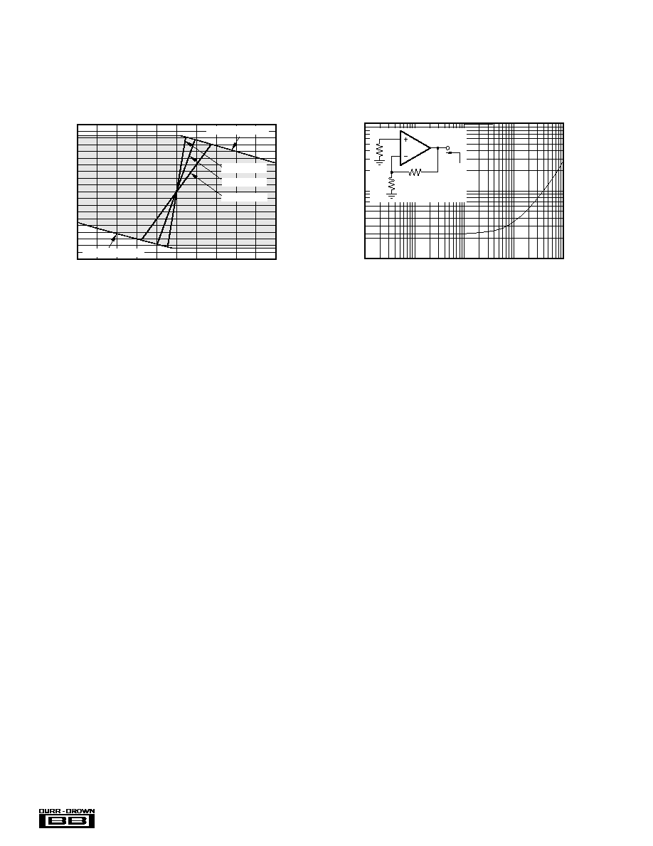
WIDEBAND CURRENT-FEEDBACK OPERATION
The OPA685 gives a new level of performance in wideband
current-feedback op amps. Nearly constant AC performance
over a wide gain range, along with 4200V/
µ
s slew rate,
offers a lower power, lower cost solution for high intercept
IF amplifier requirements. While optimized at a gain of 8V/
V (12dB to a matched 50
load) to give 400MHz band-
width, application from gains of 1 to 100 can be supported.
As a video line driver (gain of +2), the bandwidth extends to
900MHz, with a slew rate to support the highest pixel rates.
At gains above 20, the signal bandwidth starts to decrease
but still exceeds 50MHz up to a gain of 80V/V (32dB to a
matched 50
load). Single +5V supply operation is also
supported with similar bandwidths, but reduced output power
capability. For lower speed (< 250MHz) requirements at
higher output power, consider the OPA681.
Figure 1 shows the DC-coupled, gain of +8V/V, dual power
supply circuit used as the basis of the
±
5V Specifications
and Typical Performance Curves. For test purposes, the
input impedance is set to 50
with a resistor to ground and
the output impedance is set to 50
with a series output
resistor. Voltage swings reported in the specifications are
taken directly at the input and output pins, while load power
(dBm) is defined at a matched 50
load. For the circuit of
Figure 1, the total effective load will be 100
|| 458
= 82
.
The disable control line (DIS) is typically left open to
guarantee normal amplifier operation. One optional compo-
nent is included in Figure 1. In addition to the usual power
supply de-coupling capacitors to ground, a 0.1
µ
F capacitor
is included between the two power supply pins. In practical
PC board layouts, this optional capacitor will typically
improve the 2nd harmonic distortion performance by 3dB to
6dB for bipolar supply operation.
Figure 2 shows the DC-coupled, gain of 8V/V, dual power
supply circuit used as the basis of the Inverting Typical
Performance Curves. Inverting operation offers several per-
formance benefits. Since there is no common-mode signal
across the input stage, the slew rate for inverting operation
is higher and the distortion performance is slightly im-
proved. An additional input resistor, R
T
, is included in
Figure 2 to set the input impedance equal to 50
. The
parallel combination of R
T
and R
G
set the input impedance.
Both the non-inverting and inverting applications of Figures
1 and 2 will benefit from optimizing the feedback resistor
value for bandwidth (see the discussion in Setting Resistor
Values to Optimize Bandwidth). As the gain increases for
the inverting configuration, a point will be reached where
R
G
will equal 50
; R
T
is removed with the input match set
by R
G
only. With R
G
fixed to achieve an input match of
50
, to increase gain, R
F
is simply increased to get higher
gain. This will, however, quickly reduce the achievable
bandwidth as shown by the inverting gain of 16 frequency
response in the Typical Performance Curves. For gains >
12V/V (15.5dB at the matched load), non-inverting opera-
tion will give a higher bandwidth.
FIGURE 1. DC-Coupled, G = +8V/V, Bipolar Supply
Specifications and Test Circuit.
FIGURE 2. DC-Coupled, G = 8V/V, Bipolar Supply
Specifications and Test Circuit.
OPA685
+5V
DIS
5V
50
Load
50
50
V
I
50
Source
R
G
56.2
R
F
402
+
6.8
µ
F
0.1
µ
F
+
6.8
µ
F
0.1
µ
F
0.1
µ
F
OPA685
+5V
+V
S
V
S
DIS
5V
50
Load
50
20
R
T
562
R
G
54.9
+
6.8
µ
F
0.1
µ
F
+
6.8
µ
F
0.1
µ
F
0.1
µ
F
V
I
50
Source
R
F
442
14
®
OPA685
Figure 3 shows the ACcoupled, single +5V supply, gain of
+8V/V circuit configuration used as the basis for the +5V
only Specifications and Typical Performance Curves. The
key requirement of broadband single-supply operation is
maintaining input and output signal swings within the speci-
fied useable voltage ranges. The circuit in Figure 3 estab-
lishes an input midpoint bias using a simple resistive divider
from the +5V supply (two 806
resistors) to the non-
inverting input. The input signal is then AC-coupled into this
midpoint voltage bias. The input voltage can swing to within
1.7V of either supply pin, giving a 1.4Vp-p input signal
range centered around the +5V supply midpoint. The input
impedance matching resistor (57.6
) used in Figure 3 is
adjusted to give a 50
input match when the parallel
combination of the biasing divider network is included. The
gain resistor (R
G
) is AC-coupled, giving the circuit a DC
gain of +1, which puts the input DC bias voltage (2.5V) at
the output as well. The feedback resistor value has been
adjusted from the bipolar supply condition to re-optimize for
a flat frequency response in +5V only, gain of +8, operation
(see Setting Resistor Values to Optimize Bandwidth section
of this data sheet). On a single +5V supply, the output
voltage can swing to within 1.4V of either supply pin while
delivering more than 70mA output current, giving a 2.2V
output swing into 100
(5dBm maximum at the matched
load). The circuit of Figure 3 shows a blocking capacitor
driving into a 50
output resistor, then into a 50
load.
Alternatively, the blocking capacitor could be removed if
the load is tied to a supply midpoint, or to ground if the DC
current required by the load is acceptable.
Figure 4 shows the AC-coupled, single +5V supply, gain of
8V/V circuit configuration used as the basis for the +5V
only Typical Performance Curves. In this case, the midpoint
DC bias on the non-inverting input is also decoupled with an
additional 0.1
µ
F decoupling capacitor. This reduces the
source impedance at higher frequencies for the non-invert-
ing input bias current noise. This 2.5V bias on the non-
inverting input pin also appears on the inverting input pin
and, since R
G
is DC-blocked by the input capacitor, will also
appear at the output pin. One advantage to inverting opera-
tion is that since there is no signal swing across the input
stage, higher slew rates and operation at even lower supply
voltages is possible. To retain a 1Vp-p output capability,
operation down to a +3V supply is allowed. At a +3V
supply, the input common-mode range is 0V, but for the
inverting configuration of a current feedback amplifier,
wideband operation is retained even with the input stage
saturated. The circuit in Figure 4 can be operated down to a
3V supply with > 200MHz, 1Vp-p output.
FIGURE 3. AC-Coupled, G = +8V/V, Single-Supply Specifications and Test Circuit.
FIGURE 4. AC-Coupled, G = 8V/V, Single-Supply Specifications and Test Circuit.
OPA685
+5V
+V
S
DIS
50
Load
50
R
G
50
806
806
57.6
0.1
µ
F
+
6.8
µ
F
0.1
µ
F
0.1
µ
F
0.1
µ
F
V
I
V
O
50
Source
R
F
348
OPA685
+5V
+V
S
DIS
50
Load
50
R
G
50
806
806
20
0.1
µ
F
0.1
µ
F
0.1
µ
F
V
O
V
I
R
F
400
+
6.8
µ
F
0.1
µ
F

15
®
OPA685
RF SPECIFICATIONS AND
APPLICATIONS
The ultra-high full power bandwidth and 3rd-order intercept
of the OPA685 may be used to good advantage in IF
amplifier applications. Additional benefits in using a
wideband op amp such as the OPA685 include extremely
good (and independent) I/O impedance matching as well as
very high reverse isolation. A designer accustomed to using
fixed-gain RF amplifiers will get almost perfect gain accu-
racy, much higher I/O return loss, and 3rd-order intercept
points exceeding 40dBm (up to 50MHz) using only 12mA
supply current for the OPA685. Using the considerable
design freedom given by adjusting the external resistors, the
OPA685 can replace a wide range of fixed-gain RF ampli-
fiers with a single part. To understand in RF amplifier terms
how to take advantage of this, first consider the four `S'
parameters (this will be done using the example circuits of
Figures 1 and 2 on
±
5V supplies. However, similar results
can be obtained on a single +5V supply).
INPUT RETURN LOSS (S
11
)
This is a measure of how closely (over frequency) the input
impedance matches the source impedance. This is relatively
independent of gain setting for both the non-inverting and
inverting configurations. The Typical Performance Curves
show the magnitude of S
11
through 1GHz for the circuits of
Figures 1 and 2 (non-inverting gain of +8 and inverting gain
of 8 operation, respectively). Non-inverting operation of-
fers better matching to higher frequencies with the only
deviation due to the parasitic input capacitance of the non-
inverting input. The non-inverting input match is set simply
by the resistor to ground on the non-inverting input since the
amplifier itself shows a very high input impedance. Invert-
ing operation is also very good, but S
11
rises more quickly
due to loop gain roll-off effects appearing at the inverting
node. The inverting mode input match is set by the parallel
combination of R
G
and R
T
in Figure 2 since the inverting
amplifier node may be considered a virtual ground. A good
fixed-gain RF amplifier would have an input Voltage Stand-
ing Wave Ratio (VSWR) < 1.2:1. This corresponds to an S
11
of 21dB. The OPA685 exceeds this performance through
100MHz for the inverting mode of operation and through
250MHz for the non-inverting.
OUTPUT RETURN LOSS (S
22
)
This is a measure of how closely (over frequency) the output
impedance matches the load impedance. This is relatively
independent of gain for both non-inverting and inverting
operation. To first-order, the output matching impedance is
simply set by adding a series resistor to the low impedance
output of the op amp. Since the op amp itself shows a very
low output impedance which increases with frequency, an
improvement in the output match can be obtained by adding
a small equalizing capacitor across this output resistor. The
Typical Performance Curves show the measured S
22
with
and without this 3.3pF capacitor across the 50
output
resistor. Again, a very good match for a fixed-gain RF
amplifier would be a VSWR of 1.2:1. Looking at the Typical
Performance Curves for S
22
and where it rises above 21dB,
the OPA685 exceeds this level of performance through
100MHz without the equalizing capacitor and through
250MHz with it.
FORWARD GAIN (S
21
)
In all high-speed amplifier data sheets, this is referred to as
the small-signal gain which is plotted over frequency. The
difference between non-inverting and inverting operation is
that the phase of S
21
starts out at 0
°
for the non-inverting and
180
°
for the inverting. This initial phase shift for inverting
mode is inconsequential to most IF strip applications. The
phase of OPA685 is shown in the Typical Performance
Curves as a part of the gain flatness curve. It is very linear
with frequency and may be accurately modeled as a constant
time delay through the amplifier.
The Typical Performance Curves for the OPA685 show S
21
over a range of signal gains where the external resistors have
been adjusted to re-optimize flatness at each gain setting.
Since this is a current-feedback op amp, the signal bandwidth
can be held relatively constant as the desired gain setting is
changed. The "Non-Inverting Small-Signal Frequency Re-
sponse" curve shows some change in bandwidth versus gain
(due to parasitic capacitive effects on the inverting node)
with very little variation for inverting operation.
Signal gains are most often referred to as V/V in op amp data
sheets. This is the voltage gain from input to output and is
set by external resistor ratios. Since the output impedance is
set by a physical series resistor, the voltage gain to the
matched load is cut in half by this resistor divider (Figures
1 and 2). The log gain to the matched load for the non-
inverting circuit of Figure 1 is:
(1)
The log gain to the matched load for the inverting circuit of
Figure 2 is:
(2)
The specific resistor values used in Figures 1 and 2 give both
a maximally flat bandwidth and a log gain to the matched
load of 12dB. The design tables at the end of this section
summarize the required resistor values over a range of
desired gains for the circuits of Figures 1 and 2.
As the desired signal gain increases, the achievable band-
width will decrease. In the non-inverting case, it decreases
relatively quickly, as shown in the Typical Performance
Curves. The inverting configuration holds almost constant
bandwidth (with correctly selected external resistor values)
until R
G
reduces to 50
and remains at that value to satisfy
the input impedance matching requirement. Further increases
in gain are achieved by increasing R
F
, shown in Figure 2.
The bandwidth then decreases rapidly as shown by the gain
of 16V/V plot in the Typical Performance Curves.
G
R
R
dB
F
G
+
=
+
20
1
2
1
log
G
R
R
dB
F
G
log
=
20
1
2

16
®
OPA685
REVERSE ISOLATION (S
12
)
This is a measure of how much power injected into the
output matching resistor appears at the input. This is rarely
specified for an op amp because it is so good. Op amps are
very nearly uni-directional signal devices. The Typical Per-
formance Curves show this performance in the "Isolation
Characteristics vs Frequency" curve. Below 300MHz, the
non-inverting configuration of Figure 1 gives much better
isolation than the inverting of Figure 2. However, both are
well below 40dB isolation through 350MHz. Shown also on
this plot is the forward isolation for S
21
when the OPA685
is disabled. This also stays under 40dB up to 700MHz. This
specification is not shown for the inverting mode since the
signal will couple directly through the external resistors
when the amplifier is disabled for the circuit of Figure 2. If
off-isolation is a concern, the non-inverting configuration
would be preferred.
DYNAMIC RANGE LIMITS
The next consideration for RF amplifier applications are
what limits to dynamic range may be defined. Typical fixed-
gain RF amplifiers include:
1dB compression (a measure of maximum output power)
2-tone, 3rd order, output intermodulation intercept (a mea-
sure of achievable Spurious Free Dynamic Range, SFDR)
Noise Figure (NF, a measure of degradation in signal-to-
noise ratio in passing through the amplifier)
1dB Compression
The 1dB compression power is defined as the output power
at which the actual power is 1dB less than the input power
plus the log gain. In classic RF amplifiers, this is typically
10dB less than the 3rd-order intercept. This does not hold for
op amps since their intercepts are considerably improved by
loop gain and exceed the 1dB compression by much more
than 10dB. A simple estimate for 1dB compression for the
OPA685 is the maximum non-slew limited output voltage
swing available at the matched load converted into power
with 1dB added to satisfy the definition. For the OPA685 on
±
5V supplies, the output will deliver
±
3.6V at the output pin,
or
±
1.80V at the matched load. The conversion from Vp-p
to power (for a sine wave) is:
(3)
Converting this 3.6Vp-p swing at the load to dBm gives
15.1dBm. Adding 1dB to this (to satisfy the definition) gives
a 1dB compression of 16.1dBm for the OPA685 operating
on
±
5V supplies. This will be a good estimate for frequen-
cies that require less than the full slew rate of the OPA685.
The maximum frequency of operation given an available
slew rate and desired peak output swing (at the output pin)
for a sine wave is:
( 4)
Using the 4200V/
µ
s slew rate available in the inverting
mode of operation and the 3.6V peak output swing at the
output pin, gives a maximum frequency of 186MHz. This is
the maximum frequency where the 1dB compression would
be 16.1dBm at the matched load. Higher useable bandwidths
are possible at lower output power, as shown in the large-
signal bandwidth curves. As those curves show, 7Vp-p
outputs are possible with almost perfect frequency response
flatness through 100MHz for both non-inverting or inverting
operation.
Two-Tone, 3rd-Order Output Intermodulation Intercept (OP3)
In narrowband IF strips, each amplifier typically feeds into
a bandpass filter that attenuates most harmonic distortion
terms. The most troublesome remaining distortion is the
3rd-order, 2-tone intermodulations that can fall very close in
frequency to the desired signals and cannot be filtered out.
If two test frequencies are defined at f
O
+
f and f
O
f, the
3rd-order intermodulation distortion products will fall at f
O
+ 3
f and f
O
3
f. If the two test power (P
T
) levels are
equal, the OPA685 will produce 3rd-order products (P
S
) that
are at these frequencies and at a power level below the test
power levels given by:
(5)
The "Two-Tone, 3rd-Order Intermodulation Intercept" curve
shown in the Typical Performance Curves shows a very
high intercept at low frequencies, that decreases with in-
creasing frequency. This intercept is defined at the matched
load to allow direct comparison with fixed-gain RF ampli-
fiers. To produce a 2Vp-p total, 2-tone envelope at the
matched load, each power level must be 4dBm at the
matched load (1Vp-p). Using Equation 5 and the perfor-
mance curve for inverting operation, at 50MHz (41.5dBm
intercept), the 3rd-order spurious will be 2 · (41.5-4) =
75dB below these 4dBm test tones. This is exceptionally
low distortion for an amplifier that only uses 12mA supply
current. Considerable improvement from this level of per-
formance is also possible if the output drives directly into
the lighter load of an ADC input (see Differential ADC
Driver section of this data sheet).
This very high intercept versus quiescent power is achieved
by the high loop gain of the OPA685. This loop gain does,
however, decrease with frequency giving the decreasing
output intercept performance shown in the Typical Perfor-
mance Curves. Application as an IF amplifier through
200MHz is possible with output intercepts exceeding 21dBm
at 200MHz. Intercept performance will vary slightly with
gain setting decreasing at higher gains (than the 8V/V or
12dB gain used in the Typical Performance Curves) and
increasing at lower gains.
NOISE FIGURE
All fixed-gain RF amplifiers show good Noise Figure (typi-
cally < 5dB). For broadband RF amplifiers, this is achieved
by a low noise input transistor and an input match set by
feedback. This feedback greatly reduces the Noise Figure
P
P
OP
P
T
S
T
=
(
)
2
3
f
Slew Rate
V
MAX
p
=
2
P
dBm
V
O
(
)
log
.
=
(
)
10
2 2
0 001 50
2
p-p
17
®
OPA685
for fixed-gain RF amplifiers, but also makes the input match
dependent on load and the output match dependent on the
source impedance at the input.
The Noise Figure for an op amp is always higher than for
fixed-gain RF amplifiers due to their more complex internal
circuits (giving higher input noise voltage and current terms)
and the fact that, for simple circuits, the input match is set
resistively. What is gained is an almost perfect I/O imped-
ance match, much better load isolation, and very high 3rd
order intercepts versus quiescent power. This higher Noise
Figure can be acceptable if the OPA685 has enough gain
preceding it in the IF chain.
Op amp Noise Figure equations include at least 6 terms (see
the Noise Performance section of this data sheet) due to the
external resistors. As a point of reference, the circuit of
Figure 1 has an input Noise Figure of 14dB, while the
inverting configuration of Figure 2 has an input Noise
Figure of 11dB. At higher gains, it is typical for the inverting
Noise Figure to be slightly better than for an equivalent gain
non-inverting configuration. One easy way to improve the
Noise Figure for the non-inverting configuration of the
OPA685 is to include a 1:2 step-up transformer at the input
(Figure 5).
FIGURE 5. IF Amplifier with Improved Noise Figure.
The transformer provides a noiseless voltage gain at the
expense of higher source impedance for the OPA685's non-
inverting input current noise. The input impedance is still set
to 50
by the 200
resistor on the transformer secondary.
Using a 1:2 step-up will cut the required amplifier gain in
half for any particular desired overall gain.
The following tables summarize the recommended resistor
values and resulting Noise Figures over desired gain setting
for three circuit options for the OPA685 operated as a
precision IF amplifier. In each case, R
F
and R
G
are adjusted
for both best bandwidth and to get the required gain.
Table I.
Non-inverting circuit of Figure 1
Table II. Non-inverting circuit of Figure 5 with a 1:2 input
step up transformer
Table III. Inverting circuit of Figure 2
GAIN TO LOAD
R
F
R
G
NOISE
(dB)
(
)
(
)
FIGURE
6
478
159
17.20
7
468
134
16.55
8
458
113
15.95
9
446
96
15.40
10
433
81
14.91
11
419
68
14.47
12
402
57
14.09
13
384
48
13.76
14
363
40
13.23
15
340
33
13.23
16
314
27
13.03
17
284
21
12.86
18
252
16
12.72
19
215
12
12.60
20
174
9
12.51
TABLE I. Non-Inverting Wideband Op Amp (Figure 1).
GAIN TO LOAD
R
F
R
G
NOISE
(dB)
(
)
(
)
FIGURE
6
516
518
16.34
7
511
412
15.54
8
506
334
14.78
9
500
275
14.07
10
493
228
13.40
11
486
190
12.78
12
478
160
12.21
13
469
135
11.70
14
458
114
11.25
15
447
96
10.85
16
434
81
10.15
17
419
69
10.21
18
403
58
9.96
19
384
48
9.74
20
364
40
9.57
TABLE II. Non-Inverting with a 1:2 Input Step-Up Trans-
former (Figure 5).
GAIN TO LOAD
OPTIMUM
R
G
INPUT
NOISE
(dB)
R
F
(
)
(
)
MATCH R
T
FIGURE
6
463.27
116
87
16.94
7
454.61
101
98
16.06
8
444.91
88
114
15.16
9
434.07
77
142
14.23
10
421.95
66
199
13.24
11
408.42
57
380
12.16
12
398.11
50
Infinite
11.03
13
446.68
50
Infinite
10.92
14
501.19
50
Infinite
10.83
15
562.34
50
Infinite
10.75
16
630.96
50
Infinite
10.67
17
707.95
50
Infinite
10.61
18
794.33
50
Infinite
10.55
19
891.25
50
Infinite
10.49
20
1000.00
50
Infinite
10.45
TABLE III. Inverting Wideband RF Amplifier (Figure 2).
In all cases, exact computed values for resistors are shown.
Choose standard resistor values which are closest to those in
the tables for implementation.
OPA685
+5V
DIS
5V
50
Load
Supply decoupling
not shown.
50
R
G
200
V
I
V
O
R
F
50
Source
1:2
18
®
OPA685
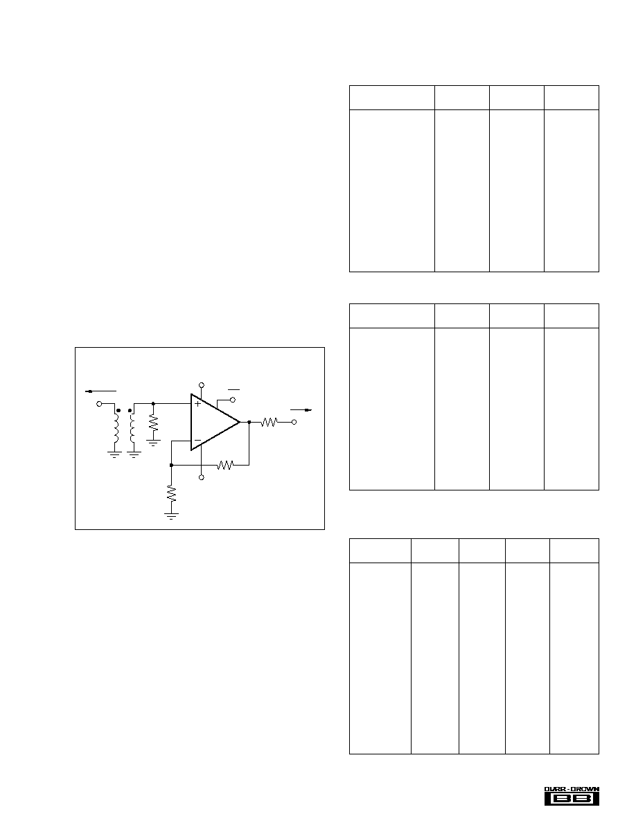
SAW FILTER BUFFER
One common requirement in an IF strip is to buffer the output
of a mixer with enough gain to recover the insertion loss of
a narrowband SAW filter. The front page of this data sheet
shows a recommended circuit using the OPA685. Operating
in the inverting mode at a voltage gain of 8V/V, this circuit
provides a 50
input match using the gain set resistor, has
the feedback optimized for maximum bandwidth (450MHz
in this case), and drives through a 50
output resistor into the
matching network at the input of the SAW filter. If the SAW
filter gives a 12dB insertion loss, a net gain of 0dB to the 50
load at the output of the SAW (which could be the input
impedance of the next IF amplifier or mixer) will be deliv-
ered in the passband of the SAW filter. Using the OPA685 in
this application will isolate the first mixer from the imped-
ance of the SAW filter and provide very low 3rd-order, 2-
tone spurious levels at the carrier frequency. Inverting opera-
tion as shown on the front page will give the broadest
bandwidth up to a gain of 12V/V (15.6dB). Non-inverting
operation will give higher bandwidth at gain settings higher
than this, but will give a slight reduction in intercept and
Noise Figure performance.
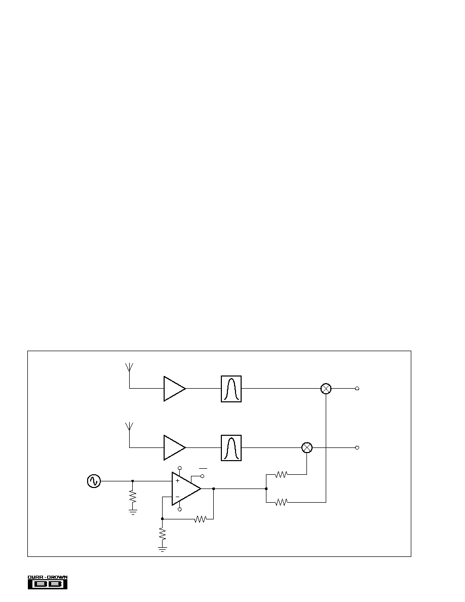
LO BUFFER AMPLIFIER
The OPA685 may also be used to buffer the Local Oscillator
(LO) from the mixer(s). Operating at a voltage gain of +2,
the OPA685 will provide almost perfect load isolation for
the LO with a net gain of 0dB to the mixer. Applications
through 1GHz LOs may be considered, but best operation
would be for LOs < 500MHz at a gain of +2. Gain could also
be easily provided by the OPA685 to drive higher power
levels into the mixer. One unique option in using the OPA685
as an LO buffer is shown in Figure 6. Since the OPA685 can
FIGURE 6. Dual Output LO Buffer.
drive multiple output loads, two identical LO signals may be
delivered to the mixers in a diversity receiver simply by
tapping the output off through two series 50
output resis-
tors. This circuit is set up for a voltage gain of +2V/V to the
output pin for a gain of +1V/V (0dB) to the mixers, but could
easily be adjusted to deliver higher gains as well.
WIDEBAND CABLE DRIVING
APPLICATIONS
The high slew rate and bandwidth of the OPA685 can be
used to meet the most demanding cable driving applications.
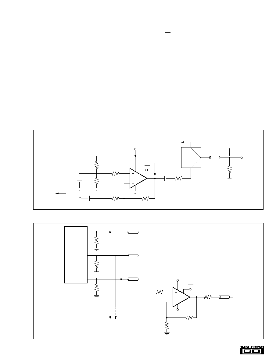
CABLE MODEM RETURN PATH DRIVER
The standard cable modem upstream driver is typically
required to drive high power over a 5MHz to 65MHz
bandwith while delivering < 50dBc distortion. Highly inte-
grated solutions (including programmable gain stages) often
fall short of this target due to high losses from the amplifier
output to the line. The higher gain operating capability of the
OPA685, along with its very high slew rate, provides a low-
cost solution for delivering this signal with the required
spurious free dynamic range. Figure 7 shows one example of
using the OPA685 as an upstream driver for a cable modem
return path. In this case, the input impedance of the driver is
set to 75
by the gain resistor (R
G
). The required input level
from the adjustable gain stage is significantly reduced by the
15.5dB gain provided by the OPA685. In this example, the
physical 75
output matching resistor, along with the 3dB
loss in the diplexer, will attenuate the output swing by 9dB
on the line. In this example, a single +12V supply was used
to achieve the lowest harmonic distortion for the 6Vp-p
OPA685
R
F
511
R
G
511
50
50
LO
50
LNA
Diversity Receiver
Antenna
Antenna
IF1
IF2
Bandpass
Filter
Bandpass
Filter
LNA
5V
+5V
DIS
Power supply decoupling not shown.
19
®
OPA685
output pin voltage through 65MHz. Measured performance
for this example gave 600MHz small-signal bandwidth and
< 54dBc distortion through 65MHz for a 6Vp-p output pin
voltage swing.
An alternative to this circuit, giving even lower distortion,
is a differential driver using two OPA685s driving into an
output transformer. This can be used either to double the
available line power, or to improve distortion by cutting the
required output swing in half for each stage. The channel
disable required by the MCNS specification should be
implemented by using the PGA disable feature. The MCNS
disable specification requires that an output impedance
match be maintained with the signal channel shut off. The
disable feature of the OPA685 is intended principally for
power savings and puts the output and inverting input pins
into a high impedance mode--this will not maintain the
required output impedance matching. Turning off the signal
at the input of Figure 7, while keeping the OPA685 active,
will maintain the impedance matching while putting very
FIGURE 7. Cable Modem Upstream Driver.
little noise on the line. The line noise in disable for the
circuit of Figure 7 (with the PGA source turned off, but still
presenting a 75
source impedance) will be a very low
4nV/
Hz (157dBm/Hz) due to the low input noise of the
OPA685.
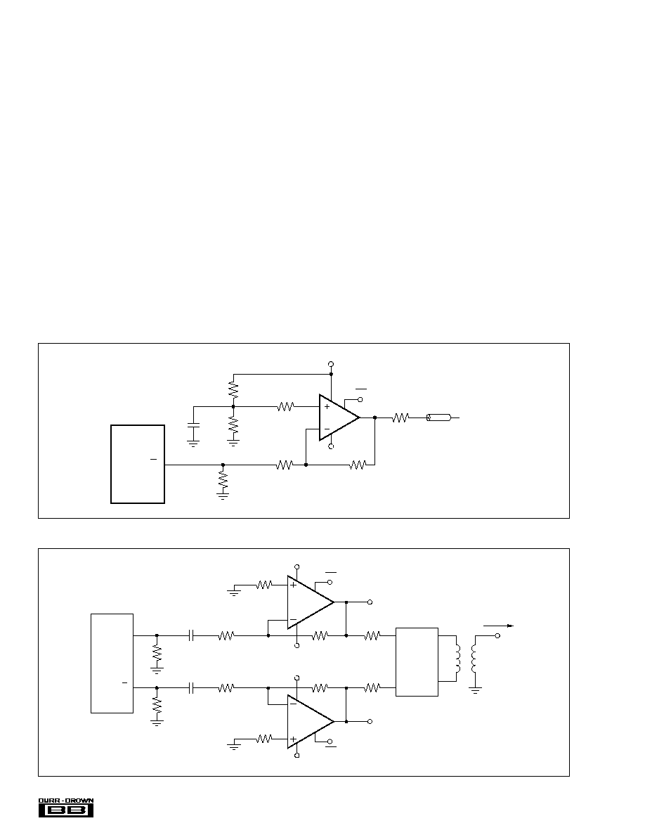
RGB VIDEO LINE DRIVER
The extremely high bandwidth of the OPA685 operating at
a gain of +2 will support the fastest RAMDAC outputs for
applications such as auxiliary monitor driving. As a general
rule, the required full power bandwidth for the amplifier
must be at least one-half the pixel rate. With its non-
inverting gain of +2, slew rate of 1900V/
µ
s, and a 1.4Vp-p
output pin voltage swing for standard RGB video levels, the
OPA685 will give a bandwidth of 400MHz, which will then
support up to 800MHz pixel rates. Figure 8 shows an
example where three OPA685s provide an auxiliary monitor
output for a high resolution RGB RAMDAC.
FIGURE 8. Gain of +2 High Resolution RGB Monitor Output.
OPA685
R
F
450
R
G
75
75
6k
6k
20
75
Diplexer
3dB
Receive Channel
Supply decoupling
not shown
67dBmV
+12V
PGA Output
58dBmV
0.1
µ
F
0.01
µ
F
0.1
µ
F
51.5dBmV
DIS
OPA685
75
75
511
R
F
511
20
+5V
Blue
5V
75
Green
RAMDAC
75
Red
Addtional
OPA685
Stages
DIS
Power supply decoupling not shown.
20
®
OPA685
An alternative circuit that will take advantage of the higher
inverting slew rate of the OPA685 (4200V/
µ
s), takes the
complementary current output from the RAMDAC and
converts it to positive video to give a very high full power
bandwidth RGB line driver. This will give sharper pixel
edges than the circuit of Figure 8. Most high-speed DACs
are current-steering designs where there is both an output
current signal that is used for the video, and a complemen-
tary output that is typically discarded into a matching resis-
tor. The complementary current output can be used as an
auxiliary output if it is inverted as shown in Figure 9.
In the circuit of Figure 9, the complementary current output
is terminated by an equivalent 75
impedance (the parallel
combination of R
T
and R
G
) that also provides a current
division to reduce the signal current through the feedback
resistor, R
F
. This allows R
F
to be increased to a value which
will hold a flat frequency response. Since the complemen-
tary current output is essentially an inverted video signal,
this circuit sets up a white video level at the output of the
OPA685 for zero DAC output current (using the 0.77V DC
bias on the non-inverting input), then inverts the comple-
mentary output current to produce a signal that ranges from
this 1.4V at zero output current down to 0V at maximum
output current level (assuming a 20mA maximum output
current). This will give a very wideband (> 400MHz) video
signal capability.
ARBITRARY WAVEFORM DRIVER
The OPA685 may be used as the output stage for moderate
output power Arbitrary Waveform Driver applications. Driv-
ing out through a series 50
matching resistor into a 50
matched load will allow up to a 3.6Vp-p swing at the
matched load (15dBm) when operating the OPA685 on a
±
5V power supply. This level of power is available for gains
of either
±
8 with a flat response through 100MHz. When
interfacing directly from a complementary current output
DAC, consider the circuit of Figure 9, modified for the peak
output currents of the particular DAC being considered.
Where purely AC-coupled output signals are required from
a complementary current output DAC, consider a push-pull
output stage using the circuit of Figure 10. The resistor
values here have been calculated for a 20mA peak output
current DAC which produces up to a 5Vp-p swing at the
matched load (18dBm). This approach will give higher
power at the load with much lower 2nd harmonic distortion.
FIGURE 9. High Resolution RGB Driver Using DAC Complementary Output Current.
FIGURE 10. High Power, Wideband AC-Coupled ARB Driver.
OPA685
+5V
5V
+5V
5V
464
66.5
0.01
µ
F
200
20
50
OPA685
464
66.5
0.01
µ
F
200
50
DAC
20mA Peak Output
Differential
Filter
I
O
I
O
50
Source
1.4:1
±
3.5V
±
3.5V
Power supply decoupling not shown.
20
DIS
DIS
OPA685
75
R
F
500
R
G
536
R
T
86.6
+5V
Power supply decoupling not shown.
5V
RAMDAC
768
4.22
0.77V
I
O
20
0.1
µ
F
DIS
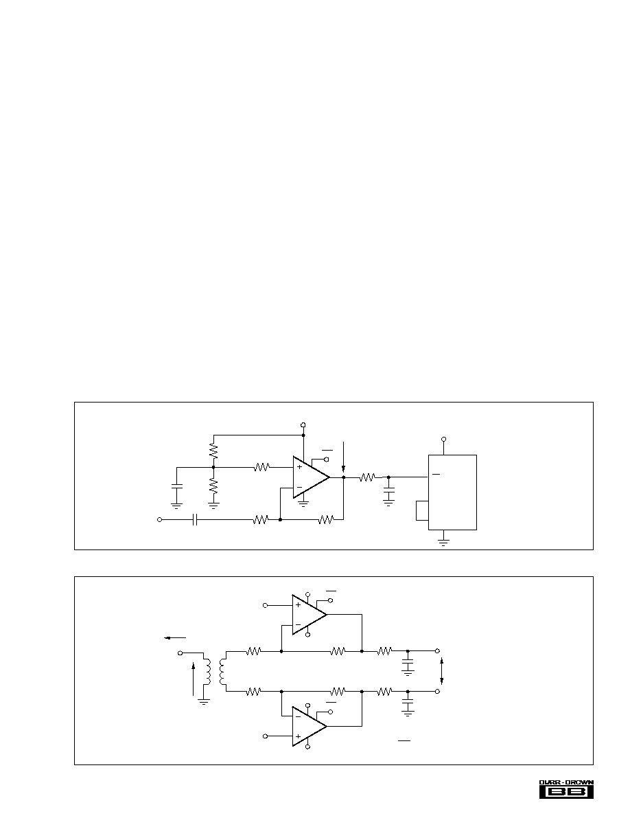
21
®
OPA685
For a 20mA peak output current DAC, the mid-scale current
of 10mA will give a 2V DC output common-mode operating
voltage due to the 200
resistor to ground at their outputs. The
total AC impedance at each output is 50
, giving a
±
0.5V
swing around this 2V common-mode voltage for the DAC.
These resistors also act as a current divider sending 75% of the
DAC output current through the feedback resistor (464
). The
blocking capacitor references the OPA685 output voltage to
ground, and turns the unipolar DAC output current into a
bipolar swing of 0.75 · 20mA · 464
= 7Vp-p at each
amplifier output. Each output is exactly 180
°
out-of-phase
from the other, producing double 7Vp-p into the matching
resistors. To limit the peak output current and improve distor-
tion, the circuit of Figure 10 is set up with a 1.4:1 step-down
transformer. This reflects the 50
load to be 100
at the
primary side of the transformer. For the maximum 14Vp-p
swing across the outputs of the two amplifiers, the matching
resistors will drop this to 7Vp-p at the input of the transformer,
then down to 5Vp-p maximum at the 50
load at the output
of the transformer.
HIGH-SPEED ADC INPUT DRIVERS
The OPA685 is ideally suited to the demanding input drive
requirements of emerging ultra high-speed and high perfor-
mance ADCs. As a single amplifier stage, 10-bit converters
through 100MSPS may be driven, while 8-bit converters
may be driven with input frequencies in excess of 100MHz.
Emerging differential input ADCs can also benefit from a
purely differential input interface using two OPA685s to get
a significant improvement in even-order harmonics along
with a somewhat improved 3rd-order harmonic suppression.
SINGLE-ENDED ADC INPUT INTERFACE
Figure 11 shows an example single +5V supply ADC driver
where the AC gain is set to 8V/V. The converter is shown
with both an inverting and non-inverting input. The inverting
input is used here to make the overall channel non-inverting.
The Typical Performance Curves for the non-inverting gain
of +8 show very flat frequency response for +5V only
operation when driving into the 20pF load capacitor shown in
Figure 11. The inverting configuration of Figure 11 was
selected for higher slew rate and lower distortion perfor-
mance. It will give > 300MHz bandwidth at this gain of 8.
Harmonic distortion for a 2Vp-p output signal will be <
50dBc through 50MHz.
DIFFERENTIAL ADC DRIVER
For applications requiring the lowest harmonic distortion
through very high frequencies, a balanced differential cir-
cuit using the OPA685 offers the best performance. Figure
12 shows an example of this approach where an input step-
up transformer is used to convert to a differential signal and
improve the Noise Figure.
FIGURE 11. Single Supply, Wideband ADC Driver.
FIGURE 12. Very Wideband Differential ADC Driver.
OPA685
42.2
V
O
= 2.5V
DC
8V
I
400
50
+5V
Power supply decoupling
not shown.
+5V
ADC
2k
2k
IN
20
0.1
µ
F
20pF
IN
CM
V
I
DIS
+5V
5V
OPA685
22pF
22pF
+5V
5V
600
OPA685
1:2
50
Source
Noise
Figure
11.8dB
V
CM
V
CM
600
100
100
43.2
Power supply decoupling
not shown.
43.2
V
I
V
O
ADC Input
V
O
V
I
= 12V/V (21.6dB)
DIS
DIS
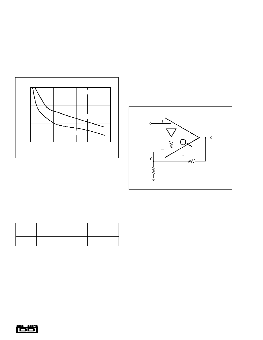
22
®
OPA685
The non-inverting inputs may be used to set the output DC
operating voltage independently of the signal path gain.
Measured single and 2-tone distortion results for the circuit
of Figure 12 are shown in Figure 13, where the outputs are
set to a +2.5V common-mode operating voltage to allow
direct coupling into a differential input, single +5V supply
ADC. This plot shows the SFDR for the worst harmonic
over frequency. The balanced differential structure of Figure
12 significantly improves SFDR at low frequencies while
holding the performance above 65dBc for a 1Vp-p output
through 60MHz.
85
80
75
70
65
60
55
5
15
25
35
45
55
65
75
Frequency (MHz)
Single and 2-T
one SFDR (dBc)
V
CM
= +2.5V
V
O
= 1Vp-p
V
O
= 2Vp-p
FIGURE 13. Measured SFDR for Differential ADC Driver
(Figure 12).
DESIGN-IN TOOLS
DEMONSTRATION BOARDS
Two PC boards are available to assist in the initial evaluation
of circuit performance using the OPA685 in its two package
styles. Both of these are available free as an unpopulated PC
board delivered with descriptive documentation. The sum-
mary information for these boards is shown below.
BOARD
LITERATURE
PART
REQUEST
PRODUCT
PACKAGE
NUMBER
NUMBER
OPA685U
SO-8
DEM-OPA68xU
MKT-351
OPA681N
SOT23-6
DEM-OPA6xxN
MKT-348
Contact the Burr-Brown applications support line to request
any of these boards.
OPERATING SUGGESTIONS
SETTING RESISTOR VALUES TO OPTIMIZE BAND-
WIDTH
A current-feedback op amp like the OPA685 can hold an
almost constant bandwidth over signal gain settings with the
proper adjustment of the external resistor values. This is
shown in the Typical Performance Curves. The small-signal
bandwidth decreases only slightly with increasing gain.
These curves also show that the feedback resistor has been
changed for each gain setting. The resistor "values" on the
inverting side of the circuit for a current-feedback op amp
can be treated as frequency response compensation elements
while their "ratios" set the signal gain. Figure 14 shows the
analysis circuit for the OPA685 small-signal frequency re-
sponse.
FIGURE 14. Current-Feedback Transfer Function Analysis
Circuit.
R
F
V
O
R
G
R
I
Z
(S)
i
ERR
i
ERR
V
I
The key elements of this current feedback op amp model are:
Buffer gain from the non-inverting input to the invert-
ing input
R
I
Buffer output impedance
i
ERR
Feedback error current signal
Z(s)
Frequency dependent open-loop transimpedance
gain from i
ERR
to V
O
The buffer gain is typically very close to 1.00 and is
normally neglected from signal gain considerations. It will,
however, set the CMRR for a single op amp differential
amplifier configuration. For the buffer gain
<
1.0, the
CMRR = 20 · log (1
).
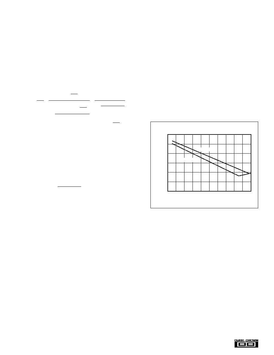
23
®
OPA685
R
I
, the buffer output impedance, is a critical portion of the
bandwidth control equation. For the OPA685, it is typically
about 19
for
±
5V operation and 23
for single +5V operation.
A current-feedback op amp senses an error current in the
inverting node (as opposed to a differential input error
voltage for a voltage-feedback op amp) and passes this on to
the output through an internal frequency dependent
transimpedance gain. The Typical Performance Curves show
this open-loop transimpedance response. This is analogous
to the open-loop voltage gain curve for a voltage-feedback
op amp. Developing the transfer function for the circuit of
Figure 14 gives Equation 6:
(6)
This is written in a loop gain analysis format where the
errors arising from a non-infinite open-loop gain are shown
in the denominator. If Z(s) were infinite over all frequen-
cies, the denominator of Equation 6 would reduce to 1 and
the ideal desired signal gain shown in the numerator would
be achieved. The fraction in the denominator of Equation 6
determines the frequency response. Equation 7 shows this as
the loop gain equation:
(7)
If 20 · log(R
F
+ NG · R
I
) were superimposed of the open-
loop transimpedance plot, the difference between the two
would be the loop gain at a given frequency. Eventually,
Z(s) rolls off to equal the denominator of Equation 7, at
which point the loop gain has reduced to 1 (and the curves
have intersected). This point of equality is where the
amplifier's closed-loop frequency response given by Equa-
tion 6 will start to roll off, and is exactly analogous to the
frequency at which the noise gain equals the open-loop
voltage gain for a voltage-feedback op amp. The difference
here is that the total impedance in the denominator of
Equation 7 may be controlled separately from the desired
signal gain (or NG).
The OPA685 is internally compensated to give a maximally
flat frequency response for R
F
= 402
at NG = 8 on
±
5V
supplies. Evaluating the denominator of Equation 7 (which
is the feedback transimpedance) gives an optimal target of
554
. As the signal gain changes, the contribution of the
NG · R
I
term in the feedback transimpedance will change,
but the total can be held constant by adjusting R
F
. Equation
8 gives an approximate equation for optimum R
F
over signal
gain:
(8)
V
O
V
I
=
1
+
R
F
R
G
1
+
R
F
+
R
I
1
+
R
F
R
G
Z
(S)
=
NG
1
+
R
F
+
R
I
NG
Z
(S)
NG
=
1
+
R
F
R
G
Z
(S)
R
F
+
R
I
NG
=
Loop Gain
As the desired signal gain increases, this equation will
eventually predict a negative R
F
. A somewhat subjective
limit to this adjustment can also be set by holding R
G
to a
minimum value of 10
. Lower values will load both the
buffer stage at the input and the output stage if R
F
gets too
low, actually decreasing the bandwidth. Figure 15 shows the
recommended R
F
versus NG for both
±
5V and a single +5V
operation. The optimum target feedback impedance for +5V
operation used in Equation 8 is 532
,
while the typical
buffer output impedance is 23
. The values for R
F
versus
gain shown here are approximately equal to the values used
to generate the Typical Performance Curves. In some cases,
the values used differ slightly from that shown here in that
the values used in the Typical Performance Curves are also
correcting for board parasitics not considered in the simpli-
fied analysis leading to Equation 8. The values shown in
Figure 15 give a good starting point for design where
bandwidth optimization is desired.
FIGURE 15. Recommended Feedback Resistor vs Noise
Gain.
The total impedance presented to the inverting input may be
used to adjust the closed-loop signal bandwidth. Inserting a
series resistor between the inverting input and the summing
junction will increase the feedback impedance (denominator
of Equation 7), decreasing the bandwidth. The internal
buffer output impedance for the OPA685 is slightly influ-
enced by the source impedance looking out of the non-
inverting input terminal. High source resistors will have the
effect of increasing R
I
, decreasing the bandwidth. For those
single-supply applications which develop a midpoint bias at
the non-inverting input through high valued resistors, the
decoupling capacitor is essential for power supply ripple
rejection, non-inverting input noise current shunting, and
minimizing the high frequency value for R
I
in Figure 14.
Inverting feedback optimization is somewhat complicated
by the impedance matching requirement at the input, as
shown in Figure 2. The resistor values shown in Table III
should be used in this case.
R
NG R
F
I
=
554
600
500
400
300
200
100
0
0
2
4
6
8
10
12
14
16
18
20
Noise Gain (V/V)
Feedback Resistor (
)
V
S
= +5V
V
S
=
±
5V

24
®
OPA685
OUTPUT CURRENT AND VOLTAGE
The OPA685 provides output voltage and current capabili-
ties that are consistent with driving doubly-terminated 50
lines. For a 100
load at the gain of +8 (see Figure 1), the
total load is the parallel combination of the 100
load and
the 456
total feedback network impedance. This 82
load
will require no more than 40mA output current to support
the
±
3.3V minimum output voltage swing specified for
100
loads. This is well under the minimum +90/60mA
guaranteed specifications.
The specifications described above, though familiar in the
industry, consider voltage and current limits separately. In
many applications, it is the voltage
·
current or V-I product,
which is more relevant to circuit operation. Refer to the
"Output Voltage and Current Limitations" plot in the Typi-
cal Performance Curves. The X and Y axes of this graph
show the zero-voltage output current limit and the zero-
current output voltage limit, respectively. The four quad-
rants provide a more detailed view of the OPA685's output
drive capabilities. Superimposing resistor load lines onto the
plot shows the available output voltage and current for
specific loads.
The minimum specified output voltage and current over-
temperature are set by worst-case simulations at the cold
temperature extreme. Only at cold startup will the output
current and voltage decrease to the numbers shown in the
guaranteed tables. As the output transistors deliver power,
their junction temperatures will increase, decreasing their
V
BE
s (increasing the available output voltage swing) and
increasing their current gains (increasing the available out-
put current). In steady-state operation, the available output
voltage and current will always be greater than that shown
in the over-temperature specifications since the output stage
junction temperatures will be higher than the minimum
specified operating ambient.
To maintain maximum output stage linearity, no output
short-circuit protection is provided. This will not normally
be a problem since most applications include a series match-
ing resistor at the output that will limit the internal power
dissipation if the output side of this resistor is shorted to
ground. However, shorting the output pin directly to the
adjacent positive power supply pin will, in most cases,
destroy the amplifier. If additional short-circuit protection is
required, consider a small series resistor in the power supply
leads. This will, under heavy output loads, reduce the
available output voltage swing. A 5
series resistor in each
power supply lead will limit the internal power dissipation
to less than 1W for an output short circuit while decreasing
the available output voltage swing only 0.25V for up to
50mA desired load currents. Always place the 0.1
µ
F power
supply decoupling capacitors directly on the supply pins
after these supply current-limiting resistors.
DRIVING CAPACITIVE LOADS
One of the most demanding, and yet very common, load
conditions for an op amp is capacitive loading. Often, the
capacitive load is the input of an A/D converter--including
additional external capacitance which may be recommended
to improve A/D linearity. A high speed, high open-loop gain
amplifier like the OPA685 can be very susceptible to de-
creased stability and closed-loop response peaking when a
capacitive load is placed directly on the output pin. When
the amplifier's open-loop output resistance is considered,
this capacitive load introduces an additional pole in the
signal path that can decrease the phase margin. Several
external solutions to this problem have been suggested.
When the primary considerations are frequency response
flatness, pulse response fidelity and/or distortion, the sim-
plest and most effective solution is to isolate the capacitive
load from the feedback loop by inserting a series isolation
resistor between the amplifier output and the capacitive
load. This does not eliminate the pole from the loop re-
sponse, but rather shifts it and adds a zero at a higher
frequency. The additional zero acts to cancel the phase lag
from the capacitive load pole, thus increasing the phase
margin and improving stability.
The Typical Performance Curves show the recommended
R
S
versus capacitive load and the resulting frequency re-
sponse at the load. Parasitic capacitive loads greater than
2pF can begin to degrade the performance of the OPA685.
Long PC board traces, unmatched cables, and connections to
multiple devices can easily cause this value to be exceeded.
Always consider this effect carefully and add the recom-
mended series resistor as close as possible to the OPA685
output pin (see Board Layout Guidelines).
DISTORTION PERFORMANCE
The OPA685 provides good distortion performance into a
100
load on
±
5V supplies. Relative to alternative solu-
tions, the OPA685 holds much lower distortion at higher
frequencies (> 20MHz) than alternative solutions. Gener-
ally, until the fundamental signal reaches very high fre-
quency or power levels, the 2nd harmonic will dominate the
distortion with a negligible 3rd harmonic component. Focus-
ing then on the 2nd harmonic, increasing the load impedance
improves distortion directly. Remember, the total load in-
cludes the feedback network. In the non-inverting configu-
ration (Figure 1), this is the sum of R
F
+ R
G
, while in the
inverting configuration, it is just R
F
. Also, providing an
additional supply decoupling capacitor (0.1
µ
F) between the
supply pins (for bipolar operation) improves the 2nd order
distortion slightly (3dB to 6dB).
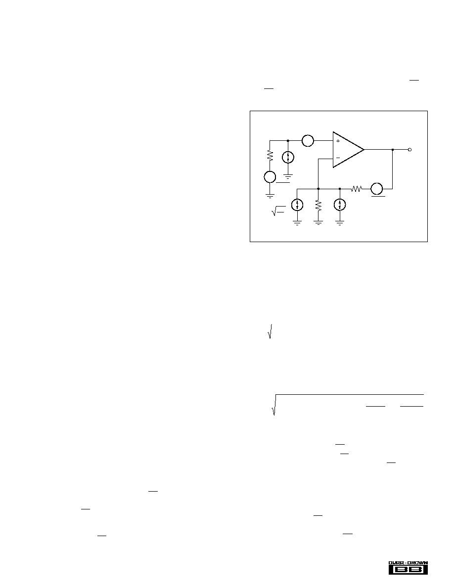
25
®
OPA685
In most op amps, increasing the output voltage swing in-
creases harmonic distortion directly. The Typical Perfor-
mance Curves show the 2nd harmonic increasing at a little
less than the expected 2x rate, while the 3rd harmonic
increases at a little less than the expected 3x rate. Where the
test power doubles, the difference between it and the 2nd
harmonic decreases less than the expected 6dB, while the
difference between it and the 3rd decreases by less than the
expected 12dB.
The OPA685 has extremely low 3rd-order harmonic distor-
tion. This also gives a high 2-tone, 3rd-order intermodulation
intercept, as shown in the Typical Performance Curves. This
intercept curve is defined at the 50
load when driven
through a 50
matching resistor to allow direct comparisons
to RF MMIC devices and is shown for both gains of
±
8.
There is a slight improvement in intercept by operating the
OPA685 in the inverting mode. The output matching resistor
attenuates the voltage swing from the output pin to the load
by 6dB. If the OPA685 drives directly into the input of a
high impedance device, such as an ADC, this 6dB attenua-
tion is not taken. Under these conditions, the intercept will
increase by a minimum 6dBm.
The intercept is used to predict the intermodulation products
for two closely-spaced frequencies. If the two test frequen-
cies, f
1
and f
2
, are specified in terms of average and delta
frequency, f
O
= (f
1
+ f
2
)/2 and
f = | f
2
f
1
| /2, the two 3rd-
order, close-in spurious tones will appear at f
O
±
3 ·
f. The
difference between two equal test-tone power levels and
these intermodulation spurious power levels is given by
dBc = 2 · (IM3 P
O
), where IM3 is the intercept taken from
the Typical Performance Curve and P
O
is the power level in
dBm at the 50
load for one of the two closely-spaced test
frequencies. For example, at 50MHz, gain of 8, the OPA685
has an intercept of 42dBm at a matched 50
load. If the full
envelope of the two frequencies needs to be 2Vp-p, this
requires each tone to be 4dBm. The 3rd-order intermodulation
spurious tones will then be 2 · (42 4) = 76dBc below the
test-tone power level (72dBm). If this same 2Vp-p 2-tone
envelope were delivered directly into the input of an ADC
without the matching loss or the loading of the 50
network,
the intercept would increase to at least 48dBm. With the same
signal and gain conditions, but now driving directly into a
light load, the 3rd-order spurious tones will then be at least
2 · (48 4) = 88dBc below the 4dBm test-tone power levels
centered on 50MHz. Tests have shown that, in reality, they
are much lower due to the lighter loading presented by most
ADCs.
NOISE PERFORMANCE
The OPA685 offers an excellent balance between voltage
and current noise terms to achieve low output noise. The
inverting current noise (19pA/
Hz) is lower than most other
current-feedback op amps while the input voltage noise
(1.7nV/
Hz) is lower than any unity gain stable, wideband,
voltage-feedback op amp. This low input voltage noise was
achieved at the price of a higher non-inverting input current
noise (13pA/
Hz). As long as the AC source impedance
looking out of the non-inverting node is less than 100
, this
4kT
R
G
R
G
R
F
R
S
OPA685
I
BI
E
O
I
BN
4kT = 1.6E 20J
at 290
°
K
E
RS
E
NI
4kTR
S
4kTR
F
current noise will not contribute significantly to the total
output noise. The op amp input voltage noise and the two
input current noise terms combine to give low output noise
under a wide variety of operating conditions. Figure 16
shows the op amp noise analysis model with all the noise
terms included. In this model, all noise terms are taken to be
noise voltage or current density terms in either nV/
Hz or
pA/
Hz.
FIGURE 16. Op Amp Noise Figure Analysis Model.
The total output spot-noise voltage can be computed as the
square root of the sum of all squared output noise voltage
contributors. Equation 9 shows the general form for the
output noise voltage using the terms shown in Figure 16.
(9)
Dividing this expression by the noise gain (NG = (1+R
F
/R
G
))
will give the equivalent input referred spot-noise voltage at
the non-inverting input as shown in Equation 10:
(10)
Evaluating these two equations for the OPA685 circuit and
component values shown in Figure 1 will give a total output
spot-noise voltage of 18nV/
Hz and a total equivalent input
spot-noise voltage of 2.3nV/
Hz. This total input referred
spot-noise voltage is higher than the 1.7nV/
Hz specifica-
tion for the op amp voltage noise alone. This reflects the
noise added to the output by the inverting current noise times
the feedback resistor. If the feedback resistor is reduced in
high gain configurations (as suggested previously), the total
input referred voltage noise given by Equation 10 will just
approach the 1.7nV/
Hz of the op amp itself. For example,
going to a gain of +20 (using R
F
= 380
)
will give a total
input referred noise of 2.0nV/
Hz.
E
O
=
E
NI
2
+
I
BN
R
S
(
)
2
+
4kTR
S
(
)
G
N
2
+
I
BI
R
F
(
)
2
+
4kTR
F
G
N
E
E
I
R
kTR
I R
NG
kTR
NG
N
NI
BN
S
S
BI
F
F
=
+
(
)
+
+
+
2
2
2
4
4
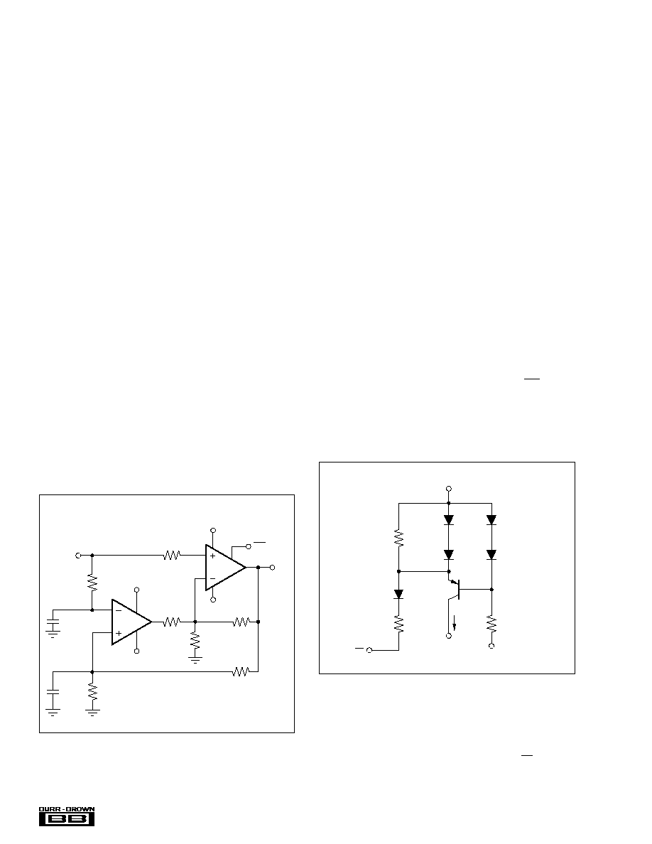
26
®
OPA685
DC ACCURACY AND OFFSET CONTROL
A current-feedback op amp like the OPA685 provides ex-
ceptional bandwidth in high gains, giving fast pulse settling
but only moderate DC accuracy. The typical specifications
show an input offset voltage comparable to high-speed
voltage-feedback amplifiers, however, the two input bias
currents are somewhat higher and are unmatched. Although
bias current cancellation techniques are very effective with
most voltage-feedback op amps, they do not generally re-
duce the output DC offset for wideband current-feedback op
amps. Since the two input bias currents are unrelated in both
magnitude and polarity, matching the source impedance
looking out of each input to reduce their error contribution
to the output is ineffective. Evaluating the configuration of
Figure 1, using worst-case +25
°
C input offset voltage and
the two input bias currents, gives a worst-case output offset
range equal to:
±
(NG
·
V
OS
) + (I
BN
·
R
S
/2
·
NG)
±
(I
BI
·
R
F
)
where NG = non-inverting signal gain
=
±
(8
·
3.5mV) + (90
µ
A
·
25
·
8)
±
(402
·
100
µ
A)
=
±
28mV + 18mV
±
40mV
= 50mV
+86mV
A fine-scale output offset null, or DC operating point adjust-
ment, is often required. Numerous techniques are available
for introducing DC offset control into an op amp circuit.
Most simple adjustment techniques do not correct for tem-
perature drift. It is possible to combine a lower speed,
precision op amp with the OPA685 to get the DC accuracy
of the precision op amp along with the signal bandwidth of
the OPA685. Figure 17 shows a non-inverting G = +10
circuit that holds an output offset voltage less than
±
1.0mV
over-temperature with > 300MHz bandwidth.
This DC-coupled circuit provides very high signal band-
width using the OPA685. At lower frequencies, the output
voltage is attenuated by the signal gain and is compared to
the original input voltage at the inputs of the OPA227 (a low
cost, precision voltage-feedback op amp with 8MHz gain
bandwidth product). If these two don't agree at low frequen-
cies, the OPA227 sums in a correcting current through the
2.55k
inverting summing path. Several design consider-
ations will allow this circuit to be optimized. First, the
feedback to the OPA227's non-inverting input must be
precisely matched to the high-speed signal gain. Making the
249
resistor to ground an adjustable resistor would allow
the low and high frequency gains to be precisely matched.
Secondly, the crossover frequency region where the OPA227
passes control to the OPA685 must occur with exceptional
phase linearity. These two issues reduce to designing for
pole/zero cancellation in the overall transfer function. Using
the 2.55k
resistor will nominally satisfy this requirement
for the circuit of Figure 17. Perfect cancellation over process
and temperature is not possible. However, this initial resistor
setting and precise gain matching will minimize long-term
pulse settling perturbations.
DISABLE OPERATION
The OPA685 provides an optional disable feature that may
be used either to reduce system power or to implement a
simple channel multiplexing operation. If the DIS control
pin is left unconnected, the OPA685 will operate normally.
To disable, the control pin must be asserted low. Figure 18
shows a simplified internal circuit for the disable control
feature.
FIGURE 17. Wideband, Precision, G = +10 Composite
Amplifier.
25k
110k
15k
I
S
Control
V
S
+V
S
V
DIS
Q1
FIGURE 18. Simplified Disable Control Circuit.
In normal operation, base current to Q1 is provided through
the 110k
resistor while the emitter current through the
15k
resistor sets up a voltage drop that is inadequate to
turn on the two diodes in Q1's emitter. As V
DIS
is pulled
LOW, additional current is pulled through the 15k
resistor,
eventually turning on these two diodes (
100
µ
A). At this
OPA685
365
2.55k
20
41.2
DIS
+5V
5V
V
O
Power supply
decoupling not shown
OPA227
5V
+5V
V
I
2.26k
249
680pF
680pF
226
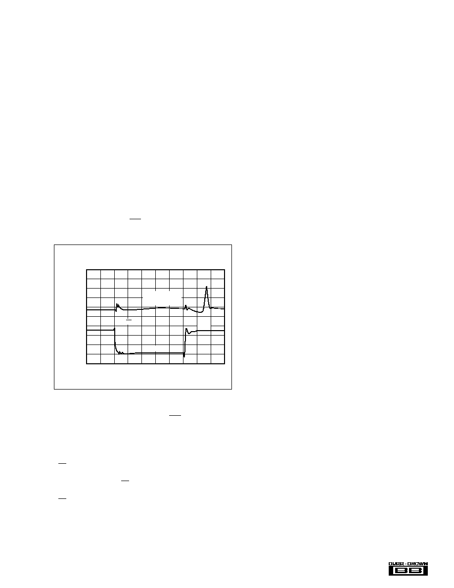
27
®
OPA685
point, any further current pulled out of V
DIS
goes through
those diodes holding the emitter-base voltage of Q1 at
approximately zero volts. This shuts off the collector cur-
rent out of Q1, turning the amplifier off. The supply current
in the disable mode are only those required to operate the
circuit of Figure 18.
When disabled, the output and input nodes go to a high
impedance state. If the OPA685 is operating in a gain of +1,
this will show a very high impedance (3pF || 1M
) at the
output and exceptional signal isolation. If operating at a
gain greater than +1, the total feedback network resistance
(R
F
+ R
G
) will appear as the impedance looking back into
the output, but the circuit will still show very high forward
and reverse isolation. If configured as an inverting ampli-
fier, the input and output will be connected through the
feedback network resistance (R
F
+ R
G
), giving relatively
poor input to output isolation.
One key parameter in disable operation is the output glitch
when switching in and out of the disabled mode. Figure 19
shows these glitches for the circuit of Figure 1 with the
input signal set to 0V. The glitch waveform at the output pin
is plotted along with the DIS pin voltage.
described below. In no case should the maximum junction
temperature be allowed to exceed 175
°
C.
Operating junction temperature (T
J
) is given by T
A
+ P
D
·
JA
.
The total internal power dissipation (P
D
) is the sum of quies-
cent power (P
DQ
) and additional power dissipated in the output
stage (P
DL
) to deliver load power. Quiescent power is simply
the specified no-load supply current times the total supply
voltage across the part. P
DL
will depend on the required output
signal and load. However, for a grounded resistive load, P
DL
would be at a maximum when the output is fixed at a voltage
equal to one-half of either supply voltage (for equal bipolar
supplies). Under this condition, P
DL
= V
S
2
/(4 · R
L
), where R
L
includes feedback network loading.
Note that it is the power in the output stage and not into the
load that determines internal power dissipation.
As an absolute worst-case example, compute the maximum
T
J
using an OPA685N (SOT23-6 package) in the circuit of
Figure 1 operating at the maximum specified ambient tem-
perature of +85
°
C and driving a grounded 100
load.
P
D
= 10V · 13.5mA + 5
2
/(4 · (100
|| 458
)) = 211mW
Maximum T
J
= +85
°
C + (0.21W · 150
°
C/W) = 117
°
C
This maximum operating junction temperature is well below
most system level targets. Most applications will be lower
since an absolute worst-case output stage power was as-
sumed in this calculation.
BOARD LAYOUT GUIDELINES
Achieving optimum performance with a high frequency
amplifier like the OPA685 requires careful attention to
board layout parasitics and external component types. Rec-
ommendations that will optimize performance include:
a) Minimize parasitic capacitance to any AC ground for
all of the signal I/O pins. Parasitic capacitance on the
output and inverting input pins can cause instability; on the
non-inverting input, it can react with the source impedance
to cause unintentional bandlimiting. To reduce unwanted
capacitance, a window around the signal I/O pins should be
opened in all of the ground and power planes around those
pins. Otherwise, ground and power planes should be unbro-
ken elsewhere on the board.
b) Minimize the distance (< 0.25") from the power
supply pins to high frequency 0.1
µ
F decoupling capaci-
tors. At the device pins, the ground and power plane layout
should not be in close proximity to the signal I/O pins. Avoid
narrow power and ground traces to minimize inductance
between the pins and the decoupling capacitors. The power
supply connections should always be decoupled with these
capacitors. An optional supply-decoupling capacitor across
the two power supplies (for bipolar operation) will improve
2nd harmonic distortion performance. Larger (2.2
µ
F to
6.8
µ
F) decoupling capacitors, effective at lower frequency,
should also be used on the main supply pins. These may be
placed somewhat farther from the device and may be shared
among several devices in the same area of the PC board.
Time (10ns/div)
Output Voltage (100mV/div)
0.2V
4.8V
Output Voltage
(0V Input)
V
DIS
+300
+200
+100
0
100
FIGURE 19. Disable/Enable Glitch.
The transition edge rate (dv/dt) of the DIS control line will
influence this glitch. For the plot of Figure 19, the edge rate
was reduced until no further reduction in glitch amplitude
was observed. This approximately 2V/ns maximum slew
rate may be achieved by adding a simple RC filter into the
V
DIS
pin from a higher speed logic line. If extremely fast
transition logic is used, a 2k
series resistor between the
logic gate and the V
DIS
input pin will provide adequate
bandlimiting using just the parasitic input capacitance on the
V
DIS
pin while still ensuring adequate logic level swing.
THERMAL ANALYSIS
The OPA685 does not require external heatsinking for most
applications. Maximum desired junction temperature will
set the maximum allowed internal power dissipation as
28
®
OPA685
c) Careful selection and placement of external compo-
nents will preserve the high frequency performance of
the OPA685. Resistors should be a very low reactance type.
Surface-mount resistors work best and allow a tighter overall
layout. Metal-film and carbon composition, axially-leaded
resistors can also provide good high frequency performance.
Again, keep their leads and PC board trace length as short as
possible. Never use wirewound-type resistors in a high
frequency application. Since the output pin and inverting
input pin are the most sensitive to parasitic capacitance,
always position the feedback and series output resistor, if
any, as close as possible to the output pin. Other network
components, such as non-inverting input termination resis-
tors, should also be placed close to the package. Where
double-side component mounting is allowed, place the feed-
back resistor directly under the package on the other side of
the board between the output and inverting input pins. The
frequency response is primarily determined by the feedback
resistor value, as described previously. Increasing its value
will reduce the bandwidth, while decreasing it will give a
more peaked frequency response. The 402
feedback resis-
tor (used in the typical performance specifications at a gain
of +8 on
±
5V supplies) is a good starting point for design.
Note that a 523
feedback resistor, rather than a direct short,
is required for the unity gain follower application. A current-
feedback op amp requires a feedback resistor--even in the
unity gain follower configuration--to control stability.
d) Connections to other wideband devices on the board
may be made with short direct traces or through on-
board transmission lines. For short connections, consider
the trace and the input to the next device as a lumped
capacitive load. Relatively wide traces (50mils to 100mils)
should be used, preferably with ground and power planes
opened up around them. Estimate the total capacitive load
and set R
S
from the plot of "Recommended R
S
vs Capacitive
Load". Low parasitic capacitive loads (< 5pF) may not need
an R
S
since the OPA685 is nominally compensated to
operate with a 2pF parasitic load. If a long trace is required,
and the 6dB signal loss intrinsic to a doubly-terminated
transmission line is acceptable, implement a matched im-
pedance transmission line using microstrip or stripline tech-
niques (consult an ECL design handbook for microstrip and
stripline layout techniques). A 50
environment is usually
not necessary on board. In fact, a higher impedance environ-
ment will improve distortion as shown in the distortion
versus load plots. With a characteristic board trace imped-
ance defined (based on board material and trace dimen-
sions), a matching series resistor into the trace from the
output of the OPA685 is used. A terminating shunt resistor
at the input of the destination device is used as well.
Remember also that the terminating impedance will be the
parallel combination of the shunt resistor and the input
impedance of the destination device; this total effective
impedance should be set to match the trace impedance. The
high output voltage and current capability of the OPA685
allows multiple destination devices to be handled as separate
transmission lines, each with their own series and shunt
terminations. If the 6dB attenuation of a doubly-terminated
transmission line is unacceptable, a long trace can be series-
terminated at the source end only. Treat the trace as a
capacitive load in this case and set the series resistor value
as shown in the plot of "R
S
vs Capacitive Load". This will
not preserve signal integrity as well as a doubly-terminated
line. If the input impedance of the destination device is low,
there will be some signal attenuation due to the voltage
divider formed by the series output into the terminating
impedance.
e) Socketing a high-speed part like the OPA685 is not
recommended. The additional lead length and pin-to-pin
capacitance introduced by the socket can create an ex-
tremely troublesome parasitic network which can make it
almost impossible to achieve a smooth, stable frequency
response. Best results are obtained by soldering the OPA685
onto the board.
INPUT AND ESD PROTECTION
The OPA685 is built using a very high-speed, complemen-
tary bipolar process. The internal junction breakdown volt-
ages are relatively low for these very small geometry de-
vices. These breakdowns are reflected in the Absolute Maxi-
mum Ratings table where an absolute maximum 13V supply
is reported. All device pins have limited ESD protection
using internal diodes to the power supplies as shown in
Figure 20.
External
Pin
+V
CC
V
CC
Internal
Circuitry
FIGURE 20. Internal ESD Protection.
These diodes also provide moderate protection to input
overdrive voltages above the supplies. The protection diodes
can typically support 30mA continuous current. Where higher
currents are possible (e.g., in systems with
±
15V supply
parts driving into the OPA685), current-limiting series resis-
tors should be added into the two inputs. Keep these resistor
values as low as possible since high values degrade both
noise performance and frequency response.